CN1229871C - 加强光放出的微发光二极管阵列 - Google Patents
加强光放出的微发光二极管阵列 Download PDFInfo
- Publication number
- CN1229871C CN1229871C CNB008166013A CN00816601A CN1229871C CN 1229871 C CN1229871 C CN 1229871C CN B008166013 A CNB008166013 A CN B008166013A CN 00816601 A CN00816601 A CN 00816601A CN 1229871 C CN1229871 C CN 1229871C
- Authority
- CN
- China
- Prior art keywords
- light
- emitting diode
- layer
- little light
- dispersion layer
- Prior art date
- Legal status (The legal status is an assumption and is not a legal conclusion. Google has not performed a legal analysis and makes no representation as to the accuracy of the status listed.)
- Expired - Lifetime
Links
- 238000003491 array Methods 0.000 title abstract description 3
- 238000000605 extraction Methods 0.000 title abstract 4
- 239000006185 dispersion Substances 0.000 claims description 72
- 239000000758 substrate Substances 0.000 claims description 37
- 239000004065 semiconductor Substances 0.000 claims description 24
- 230000004888 barrier function Effects 0.000 claims description 18
- 229910052751 metal Inorganic materials 0.000 claims description 14
- 239000002184 metal Substances 0.000 claims description 14
- 238000009413 insulation Methods 0.000 claims description 7
- 238000000034 method Methods 0.000 abstract description 23
- 230000001965 increasing effect Effects 0.000 abstract description 9
- 229910052737 gold Inorganic materials 0.000 description 14
- 238000010276 construction Methods 0.000 description 13
- 239000000463 material Substances 0.000 description 13
- 239000011159 matrix material Substances 0.000 description 12
- 238000005516 engineering process Methods 0.000 description 8
- 238000005530 etching Methods 0.000 description 8
- 229910052763 palladium Inorganic materials 0.000 description 7
- 238000001020 plasma etching Methods 0.000 description 7
- 229910052697 platinum Inorganic materials 0.000 description 7
- 229910010271 silicon carbide Inorganic materials 0.000 description 6
- 239000004020 conductor Substances 0.000 description 5
- 230000003993 interaction Effects 0.000 description 5
- 229920000642 polymer Polymers 0.000 description 5
- VYPSYNLAJGMNEJ-UHFFFAOYSA-N Silicium dioxide Chemical compound O=[Si]=O VYPSYNLAJGMNEJ-UHFFFAOYSA-N 0.000 description 4
- 229910052759 nickel Inorganic materials 0.000 description 4
- 229910052594 sapphire Inorganic materials 0.000 description 4
- 239000010980 sapphire Substances 0.000 description 4
- 229910000980 Aluminium gallium arsenide Inorganic materials 0.000 description 3
- 229910045601 alloy Inorganic materials 0.000 description 3
- 239000000956 alloy Substances 0.000 description 3
- 230000008901 benefit Effects 0.000 description 3
- 238000000151 deposition Methods 0.000 description 3
- 238000004519 manufacturing process Methods 0.000 description 3
- 150000004767 nitrides Chemical class 0.000 description 3
- 230000000737 periodic effect Effects 0.000 description 3
- 238000007639 printing Methods 0.000 description 3
- 230000001902 propagating effect Effects 0.000 description 3
- 230000000717 retained effect Effects 0.000 description 3
- 229910052709 silver Inorganic materials 0.000 description 3
- 239000000126 substance Substances 0.000 description 3
- 229910001218 Gallium arsenide Inorganic materials 0.000 description 2
- 239000004793 Polystyrene Substances 0.000 description 2
- 238000002679 ablation Methods 0.000 description 2
- 238000010521 absorption reaction Methods 0.000 description 2
- 230000005540 biological transmission Effects 0.000 description 2
- 230000008859 change Effects 0.000 description 2
- 238000005229 chemical vapour deposition Methods 0.000 description 2
- 238000001312 dry etching Methods 0.000 description 2
- 230000000694 effects Effects 0.000 description 2
- 230000008020 evaporation Effects 0.000 description 2
- 238000001704 evaporation Methods 0.000 description 2
- 239000010408 film Substances 0.000 description 2
- 238000010438 heat treatment Methods 0.000 description 2
- 230000006872 improvement Effects 0.000 description 2
- 238000002955 isolation Methods 0.000 description 2
- 229920002223 polystyrene Polymers 0.000 description 2
- 230000008569 process Effects 0.000 description 2
- 238000004064 recycling Methods 0.000 description 2
- 230000011218 segmentation Effects 0.000 description 2
- 239000000377 silicon dioxide Substances 0.000 description 2
- 239000010409 thin film Substances 0.000 description 2
- 238000005452 bending Methods 0.000 description 1
- 230000008033 biological extinction Effects 0.000 description 1
- 229910052681 coesite Inorganic materials 0.000 description 1
- 239000002131 composite material Substances 0.000 description 1
- 150000001875 compounds Chemical class 0.000 description 1
- 229910052906 cristobalite Inorganic materials 0.000 description 1
- 238000005520 cutting process Methods 0.000 description 1
- 230000008021 deposition Effects 0.000 description 1
- 238000007599 discharging Methods 0.000 description 1
- 230000005611 electricity Effects 0.000 description 1
- 238000010894 electron beam technology Methods 0.000 description 1
- 238000005538 encapsulation Methods 0.000 description 1
- 230000002708 enhancing effect Effects 0.000 description 1
- 239000003822 epoxy resin Substances 0.000 description 1
- 230000001747 exhibiting effect Effects 0.000 description 1
- 239000012634 fragment Substances 0.000 description 1
- 239000011521 glass Substances 0.000 description 1
- 239000008187 granular material Substances 0.000 description 1
- 230000017525 heat dissipation Effects 0.000 description 1
- 238000005286 illumination Methods 0.000 description 1
- 230000008676 import Effects 0.000 description 1
- 239000012212 insulator Substances 0.000 description 1
- 230000007246 mechanism Effects 0.000 description 1
- 238000006263 metalation reaction Methods 0.000 description 1
- 238000001465 metallisation Methods 0.000 description 1
- 150000002739 metals Chemical class 0.000 description 1
- 239000004005 microsphere Substances 0.000 description 1
- 239000000203 mixture Substances 0.000 description 1
- 230000004048 modification Effects 0.000 description 1
- 238000012986 modification Methods 0.000 description 1
- 230000003287 optical effect Effects 0.000 description 1
- 230000002093 peripheral effect Effects 0.000 description 1
- 229920000647 polyepoxide Polymers 0.000 description 1
- 230000000644 propagated effect Effects 0.000 description 1
- 230000005855 radiation Effects 0.000 description 1
- 230000009467 reduction Effects 0.000 description 1
- -1 semimetal Substances 0.000 description 1
- 235000012239 silicon dioxide Nutrition 0.000 description 1
- 239000007787 solid Substances 0.000 description 1
- 238000001228 spectrum Methods 0.000 description 1
- 229910052682 stishovite Inorganic materials 0.000 description 1
- 238000005728 strengthening Methods 0.000 description 1
- 229910052905 tridymite Inorganic materials 0.000 description 1
Images


Classifications
-
- H—ELECTRICITY
- H01—ELECTRIC ELEMENTS
- H01L—SEMICONDUCTOR DEVICES NOT COVERED BY CLASS H10
- H01L33/00—Semiconductor devices with at least one potential-jump barrier or surface barrier specially adapted for light emission; Processes or apparatus specially adapted for the manufacture or treatment thereof or of parts thereof; Details thereof
- H01L33/02—Semiconductor devices with at least one potential-jump barrier or surface barrier specially adapted for light emission; Processes or apparatus specially adapted for the manufacture or treatment thereof or of parts thereof; Details thereof characterised by the semiconductor bodies
- H01L33/08—Semiconductor devices with at least one potential-jump barrier or surface barrier specially adapted for light emission; Processes or apparatus specially adapted for the manufacture or treatment thereof or of parts thereof; Details thereof characterised by the semiconductor bodies with a plurality of light emitting regions, e.g. laterally discontinuous light emitting layer or photoluminescent region integrated within the semiconductor body
-
- H—ELECTRICITY
- H01—ELECTRIC ELEMENTS
- H01L—SEMICONDUCTOR DEVICES NOT COVERED BY CLASS H10
- H01L33/00—Semiconductor devices with at least one potential-jump barrier or surface barrier specially adapted for light emission; Processes or apparatus specially adapted for the manufacture or treatment thereof or of parts thereof; Details thereof
- H01L33/36—Semiconductor devices with at least one potential-jump barrier or surface barrier specially adapted for light emission; Processes or apparatus specially adapted for the manufacture or treatment thereof or of parts thereof; Details thereof characterised by the electrodes
- H01L33/38—Semiconductor devices with at least one potential-jump barrier or surface barrier specially adapted for light emission; Processes or apparatus specially adapted for the manufacture or treatment thereof or of parts thereof; Details thereof characterised by the electrodes with a particular shape
-
- H—ELECTRICITY
- H01—ELECTRIC ELEMENTS
- H01L—SEMICONDUCTOR DEVICES NOT COVERED BY CLASS H10
- H01L33/00—Semiconductor devices with at least one potential-jump barrier or surface barrier specially adapted for light emission; Processes or apparatus specially adapted for the manufacture or treatment thereof or of parts thereof; Details thereof
- H01L33/02—Semiconductor devices with at least one potential-jump barrier or surface barrier specially adapted for light emission; Processes or apparatus specially adapted for the manufacture or treatment thereof or of parts thereof; Details thereof characterised by the semiconductor bodies
- H01L33/20—Semiconductor devices with at least one potential-jump barrier or surface barrier specially adapted for light emission; Processes or apparatus specially adapted for the manufacture or treatment thereof or of parts thereof; Details thereof characterised by the semiconductor bodies with a particular shape, e.g. curved or truncated substrate
- H01L33/22—Roughened surfaces, e.g. at the interface between epitaxial layers
-
- H—ELECTRICITY
- H01—ELECTRIC ELEMENTS
- H01L—SEMICONDUCTOR DEVICES NOT COVERED BY CLASS H10
- H01L33/00—Semiconductor devices with at least one potential-jump barrier or surface barrier specially adapted for light emission; Processes or apparatus specially adapted for the manufacture or treatment thereof or of parts thereof; Details thereof
- H01L33/36—Semiconductor devices with at least one potential-jump barrier or surface barrier specially adapted for light emission; Processes or apparatus specially adapted for the manufacture or treatment thereof or of parts thereof; Details thereof characterised by the electrodes
- H01L33/40—Materials therefor
- H01L33/42—Transparent materials
Abstract
本发明揭示了一种新的发光二极管结构,其提供增加的光放出效率。该新发光二极管结构包含电连接微发光二极管(12)的阵列,其具有一活性层(14)夹在两个相反地掺杂的层(16,18)之间。该微发光二极管形成在一第一分散层(18)之上,而该微发光二极管其下层(16)则与该第一分散层(18)相接触。一第二分散层(24)形成于该微发光二极管(12)之上,并与其上层(16)相接触。该第一分散层(18)将该第二分散层(24)电绝缘。每个分散层(20,24)皆具有一接触点(22,26),当一偏压施加到所述接触点(22,26)时,电流流到微发光二极管(12),并发光。新发光二极管的效率由增加的微发光二极管(12)的发射表面而增加。来自每个微发光二极管活性层(14)的光将会在行进一短距离之后而到达一表面,并降低该光的全内反射。位于微发光二极管(12)之间的光放出组件(LEEs)(82,84,86,88,90,92,94)可被包含来另外加强光放出。新发光二极管以标准处理技术来制造,使其易于制造,且成本类似于标准的发光二极管。
Description
本申请要求Thibeault等人于1999年12月3日申请的美国临时申请案第60/168,817号之权利。
技术领域
本发明涉及一种发光二极管,更具体地说,涉及一种加强所述发光二极管的光放出的新结构。
背景技术
发光二极管(LEDs)为一种将电能转换为光的重要固态装置,该装置通常包含一半导体材料的活性层,其夹在两个相反地掺杂层之间。当一偏压施加到该掺杂层时,空穴及电子被注入该活性层且在其中复合而产生光。由该活性区所产生的光全向发射,并且从所有暴露面逸出该装置。该发光二极管的外壳通常用来将逸出的光导入一所要求的输出发射剖面。
当半导体材料改进时,该些半导体装置的效率也有改进。新的发光二极管用像是GaN的材料制作,该材料提供了在紫外线到黄光光谱范围内的有效光照。许多新的发光二极管在转换电能到光时比传统的灯更有效率以及可更可靠。由于发光二极管改进了,其被预期可在许多应用中取代传统的灯,例如交通信号、室外及室内显示器、汽车头灯及尾灯、常规室内照明等等。
然而,传统的发光二极管的效率受限于其不能够发射所有由其活性层产生的光。当一发光二极管被通电时,由其活性层发射的光(全向地)以许多不同的角度到达发射面。典型的半导体材料与周围空气(折射指数n等于1.0)或封装的环氧树脂(n约为1.5)相比,具有一较高的折射指数(n约为2.2至3.8)。根据斯涅尔定律,光线在从一具有高折射指数的地方传播到一具有低折射指数的地方时,如该光线在某一临界角之内(相对于该曲面法线方向),将会穿过到达该指数较低的地方。该光线以大于临界角到达该曲面时则不会穿过,而会经历全内反射(TIR)。在一个发光二极管的情况下,该TIR光可不断地在该发光二极管中反射,直到其被吸收为止,或其可从不同于该发射面的表面逸出。由于此现象,大量由传统发光二极管所产生的光没有发射出去,而使效率降低。
一种降低TIR光的百分比的方法是要在发光二极管的表面上产生随机结构型式的光散射中心。[由Shnitzer等人提出,″30% External Quantum Efficiency fromSurface Textured,Thin Film Light Emitting Diodes″,Applied Physics Letters63,页2174-2176(1993)]。该随机结构是在反应离子蚀刻期间,藉由使用亚微米直径聚苯乙烯颗粒在该发光二极管表面上做为一掩模而成型于该表面上。该结构化的表面具有在光的波长方面的特点,以致光的折射及反射的方式由于该随机干扰效应而无法由斯涅尔定律来预测。此方法显示可将发射效率改善9%到30%。
该表面结构的一个缺点在于其在该些具有较差导电性的电极层构造的发光二极管,例如p-型GaN,该表面结构可妨碍有效的电流分散。在较小的装置或具有良好导电性的装置中,来自该p及n型层接触点的电流可流入传遍各个层。而对于较大的装置或以较差导电性材料制成的装置,电流无法由该接触点传遍各个层。因此,部份该活性层不能接收到该电流而不能发射光。为了要在整个二极管区域产生均匀的电流注入,一导电材料分散层可沉积在其表面上。然而,此分散层通常必须是透光的以便光线能够透过该层。当一随机表面结构被引进到该发光二极管表面上时,则不能轻易地沉积一足够薄且透光的电流分散层。
另一个增加一发光二极管的光放出的方法为包含一在该发射表面或内部界面的周期图案,其可将光线从其内部的补捉角以由该表面形状及图案来确定的限定模式来重新导向。请参考授予Krames等人的美国专利号5,779,924。此技术为一随机结构表面的一特殊例,其中该干扰效应不再是随机的,而该表面可将光耦合到特殊的模式或方向。此方法的一个缺点是该结构很难制造,因为该表面形状及样式必须是均匀的,并且非常小,小至相当于该发光二极管光的单一波长。该图案也为沉积一透光的电流分散层带来困难,如前所述。
要增加光放出也可通过将该发光二极管的放射面做成一在中心具有一放射层的半球形。在此结构增加放射光的量的同时,其的制作也很难。给Scifres及Burnham的美国专利号3,954,534中,揭示了形成一种发光二极管的阵列,在每个发光二极管之上分别有一半球形。该半球形系形成于一基板中,而二极管阵列于其上增长。然后,该二极管及透镜结构从该基板上蚀刻去除。此方法的缺点是其限于将该结构形成在该基板介面,而从该基板移除该结构会造成制造成本的增加。同时,每个半球皆有一放射层直接地位于其上,其需要非常精密的制造。
美国专利号5,793,062揭示一种结构,其用于加强自一发光二极管的光放出,藉由包含不吸光的非吸收层来将光重新导向离开吸收区域,例如接触点,并且还使光朝该发光二极管的表面方向改向。此结构的一个缺点是,该非吸收层需要形成削底的狭角层,对许多材料体系而言非常难以制造。
加强光放出的另一个方法是在该发光二极管的发射面上的一薄膜金属层之内将光子耦合到表面等离子体振子模式,该些光子被发射回到辐射模式。[Knock等人的,″Strongly Directional Emission from AlGaAs/GaAs Light EmittingDiodes″,Applied Physics Letter 57,页2327-2329,(1990)]。这些结构依赖将该半导体发射回来的光子耦合到该金属层中的表面等离子体振子,其进一步与最终被放出的光子耦合。此装置的一个缺点是,其很难制造,因为该周期结构为一沟深极浅(<0.1微米)的单维刻划光栅。同时,总体外部量子效率很低(1.4-1.5%),很可能是由于光子到表面等离子体振子以及表面等离子体振子到环境光子转换机制的效率低。此结构也会带来与一电流分散层有关的同样的困难,如上所述。
要改善光放出还可藉由使发光二极管片的侧面成某一角度以产生一倒置的截顶锥形。该成某一角度的表面提供了一在临界角之内的放射面给截留于该基板材料中的TIR光线[Krames等人的,’High Power Truncated Inverted Pyramid(AlxGal-x)0.5In0.5P/GaP Light Emitting Diodes Exhibiting>50% ExternalQuantum Efficiency’,Applied Physics Letters 75(1999)]。藉由此方法,对于InGaAlP材料体系来说,所展示的外部量子效率增加了35%到50%。此方法对于将大量光截留于该基板中的装置来说是可行的。至于在蓝宝石基板上成长GaN的情况下,大量光是被截留于GaN膜中,所以使发光二极管片的侧面成某一角度并不能达到所要求的增益。
另有一种加强光放出的方法是光子循环利用[Shnitzer等人的,’Ultrahighspontaneous emission quantum efficiency,99.7% internally and 72%externally,from AlGaAs/GaAs/AlGaAs double heterostructures’,AppliedPhysics Letters 62,页131-133,(1993)]。此方法依靠具有一高效率活性层的发光二极管,该活性层可立即将电子及空穴转换成光,反之亦然。TIR光由该发光二极管表面反射出来,并撞击到该活性层,从而转换回到一电子-空穴对。由于该活性层的高效率,该电子-空穴对几乎立即转换为光,并再次向随机方向发射。某一百分比的循环利用光将会以小于临界角来打在发光二极管的其中一个发射面而逸出。而反射回到该活性层的光会再次经历同样的过程。然而,此方法仅能够用于以光损耗非常低的材料制成的发光二极管,而不能够用于在其表面上具有一吸收电流分散层的发光二极管。
发明内容
本发明提供一种新的发光二极管,其具有互连的微发光二极管阵列,以提供改善的光放出。微发光二极管具有一较小的活性区,其范围在1到2500平方微米,但该大小并非本发明的关键。一微发光二极管的阵列为任何以电互连的微发光二极管分布。该阵列提供一大的表面积,使光能够逸出每个微发光二极管,此而增加发光二极管的可用光。所述新发光二极管可具有许多不同的几何形状,且由于其是以标准半导体处理技术来形成,故非常易于制造。
该新发光二极管包含一第一导电分散层,其的一个表面上沉积有若干微发光二极管。每个微发光二极管皆具有一p-型层,一n-型层及一夹在所述p-及n-型层之间的活性层。所述p-或n-型层皆可为上层,而另一个则可为下层。施加于所述第一分散层的电流会分散到每个微发光二极管的下层。一第二分散层包含在所述微发光二极管上,而自所述第二分散层的电流会分散到所述上层。当一偏压施加在所述第一及第二分散层时,微发光二极管即发光。
所述第二分散层的一实施例为一导电的互连的栅格状结构,其具有在所述微发光二极管上的导电通路,该些通路与所述微发光二极管的上层接触。一绝缘层包含在所述阵列上,而所述栅格在该绝缘层上,因此将所述第一分散层与所述栅格电绝缘。
另外,可用倒装片接合使微发光二极管互连。使用此方法,首先形成一未连接的微发光二极管阵列,然后使其接合到一导电性材料以使该阵列互连。在一第三实施例中,所述栅格通过微发光二极管,而且所述p-型、活性层、及n-型材料在该些微发光二极管之间的栅格的导电通路之下以将该栅格及第一分散层电绝缘。此栅格状结构可被设计来使发射的光能够在传播一段短距离之后与一侧壁互相作用。
所述新发光二极管能够使光放出组件(LEEs)沉积在该些微发光二极管之间,或是形成在该些微发光二极管的侧面之上,以进一步加强光放出。该些LEEs用来使在一标准发光二极管结构中的光线转向或聚焦,否则光线将会通过TIR被截留或吸收。LEEs的形状可以是曲面的(凸出或凹入),或是片段线性的,而该结构的形状会影响光放出以及光的最终放出方向。在所述微发光二极管之间的LEEs与从该微发光二极管侧面逸出的光相互作用。此相互作用有助于防止反射回到该发光二极管的光被吸收,因此增加了由该发光二极管出来的有用光。
通过以下的详细叙述并且结合附图,本领域的技术人员就会明白本发明的这些以及其它进一步的特征和优点,其中:
附图说明
图1所示为一具有一微发光二极管阵列的新发光二极管的平面图,该微发光二极管阵列具有一在一电绝缘层上的互连电流分散栅格;
图2所示为图1中该新发光二极管沿截面线2-2的剖面图;
图3所示为该新发光二极管的另一实施例的剖面图,其微发光二极管阵列是利用倒装式安装接合到一次固定层的;
图4所示为该新发光二极管的一第三实施例的导电互连电流分散栅格和在该格栅通路下面的半导体材料的平面图;
图5所示为图4中该发光二极管沿截面线4-4的剖面图;
图6所示为另一互连电流分散栅格的平面图;
图7所示为又一互连电流分散栅格的平面图;
图8所示为可在该微发光二极管之内结合的LEEs的基本形状的剖面图;
图9所示为具有在该些微发光二极管之间形成的不同的LEEs的该新发光二极管的剖面图,;
图10所示为具有以随机形式构造表面的LEEs的该新发光二极管的剖面图;
图11所示为图10中该微发光二极管阵列的剖面图,其具有一直接地位于该电流分散栅格下面的电流阻隔层;
图12所示为具有与微发光二极管的侧面成一体的LEEs的该新发光二极管的剖面图;
图13所示为具有与微发光二极管的侧面结合的曲面LEEs的该新发光二极管的剖面图;
图14所示为具有与微发光二极管的侧面及中间结合的曲面LEEs的该新发光二极管的剖面图;及
图15所示为如图4中的但具有曲面的LEEs的该新发光二极管的剖面图。
具体实施方式
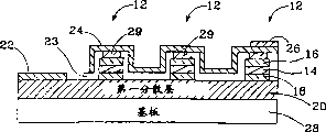
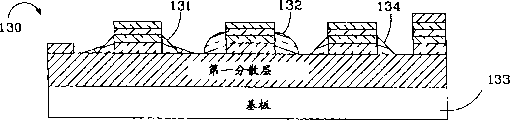
图1及2所示为根据本发明构造的该新发光二极管10的一实施例。该发光二极管包含一微发光二极管12的阵列,每个微发光二极管12皆被隔离,并具有其本身的夹在相反掺杂层16及18之间的半导体材料活性层14。在较佳的微发光二极管中,其上层16为p-型,而下层18为n-型,尽管将层16及层18相反地掺杂仍然可以运作。
该新发光二极管也包含一第一分散层20,其将电流由n-接触点22分散到每个微发光二极管的下层18。该接触点22称为n-接触点是由于在该较佳实施例中的下层18为n-型。一绝缘层23沉积在该微发光二极管阵列之上,其覆盖了每个微发光二极管以及在微发光二极管之间的沟槽中第一分散层的表面。一第二分散层,其最好以一互连电流分散栅格24的形式沉积在该绝缘层上,该绝缘层与栅格的导电通路在该些微发光二极管上横过。一p-接触点26沉积在该栅格24上,而从该接触点的电流通过该栅格分散到每个微发光二极管12的上层16。该接触点26称之为p-接触点,因为在该较佳实施例中的上层16为p-型。
一空穴形成于每个微发光二极管之上而穿过所述绝缘层,一微发光二极管接触点29包含在每个绝缘层空穴中以作为在栅格24和微发光二极管的上层16之间的接触点。所述微发光二极管(除了空穴之外)和所述第一分散层的表面通过所述绝缘层23与所述电流分散栅格电绝缘。整个结构在一基板28上形成且该些微发光二极管形成一阵列且在一偏压施加于接触点22及26时即发光。在另一实施例中,一透明导电片被用作为第二分散层来代替栅格24。
该新发光二极管10具有增强的光放射,是因为其发射面通过该些隔离的微发光二极管而增加。由每个微发光二极管的活性层所产生的光仅在一小段距离之后即与该微发光二极管的边缘相互作用。如果该光在该临界角之内,其可从微发光二极管逸出,并对该发光二极管的光放射作出贡献。新发光二极管特别有利于某些发光二极管结构,在该些结构中的部份发射光由于在电流分散层与基板介面处的全内反射(TIR)而不能传播到基板。这种状况发生在蓝宝石、AlN、或MgO基板上基于GaN的发光二极管。
新发光二极管10通过先沉积第一分散层20在基板28上来制造。然后,一具有一n-型、p-型及一活性层的外延生长的发光二极管结构在第一分散层20上形成。该微发光二极管是使用半导体蚀刻技术,例如湿式化学蚀刻,反应离子蚀刻(RIE),离子研磨,或任何其它用于移除半导体材料的技术,蚀刻去除部份发光二极管结构而形成的。
每个剩余的微发光二极管形成一独立及电绝缘的装置,其具有一由相反掺杂层16及18包围的活性层。该微发光二极管12的形状及位置皆可不同,每个微发光二极管的形状最好为圆柱形。当由上方观视时,每个微发光二极管呈现为圆形,其直径为1到50微米之间。该微发光二极管最好形成密集的结构以使可用的微发光二极管空间最大化。相邻微发光二极管之间的间距最好是在1到50μm的范围内,虽然该间距并非本发明的关键。绝缘器层23可由不同的方法来沉积在整个结构上,例如蒸发,化学气相沉积(CVD)或溅镀。然后在每个微发光二极管12上的绝缘层23中蚀出开口。微发光二极管接触点及导电栅格然后通过标准的沉积技术来沉积。
所述第一分散层20既可以是一沉积在基板上的导电层,又可是该基板本身,如果其是导电的话。基于GaN的发光二极管的较佳导电基板包含GaN或碳化硅(SiC)。SiC具有更密集的晶格而与III族氮化物相配,例如GaN,而且使III族氮化物薄膜具有高品质。碳化硅也具有一非常高的热导率,所以在碳化硅上的III族氮化物装置的整体输出功率不受限于该基板的热耗散(像一些在蓝宝石上形成的装置通常就会这样)。SiC基板可由美国North Carolina,Durham的Cree Research公司获得,其制造方法被阐明于科学文献及美国专利,有关编号为34,861;4,946,547及5,200,022。
如果该基板为电流分散层,底部接触点可通过使在该基板上暴露的任何表面金属化而沉积。较佳的发光二极管具有微发光二极管12,其基于AlGaInN且以一p-型表面作为其上层16。该基板为蓝宝石,第一分散层为n-型AlGaInN(或其合金),而金属化接触点为Al/Ni/Au、Al/Ti/Au、或Al/Pt/Au。所述绝缘层23可由许多材料制成,例如,但不限于,SiN、SiO2、或AlN。
该栅格24可以是任何导电材料,包含金属、半金属、及半导体。其可由Al、Ag、Al/Au、Ag/Au、Ti/Pt/Au、Al/Ti/Au、Al/Ni/Au、Al/Pt/Au或其组合物来制成。另外,该栅格可由一薄的半透明金属来制成,例如Pd、Pt、Pd/Au、Pt/Au、Ni/Au、NiO/Au或其合金来制成。该栅格24可由许多传统的方法而沉积在所述新发光二极管上,而较佳的方法为蒸发或溅镀。在较佳实施例中,电流分散栅格24的通路宽度在1到10μm之间。微发光二极管接触点29可用Pt、Pt/Au、Pd、Pd/Au、Ni/Au、NiO、或NiO/Au制成。p-接触点26可以沉积在所述互连栅格24上的不同位置,以使来自接触点的电流可以传遍该栅格。
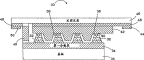
图3所示为一根据本发明来构造的发光二极管30的第二实施例,其利用倒装式安装。如上所述,是通过蚀刻去除一完整发光二极管结构的半导体材料来形成一微发光二极管32阵列的。每个微发光二极管32具有一由两个相反掺杂层所包围的活性层。微发光二极管的配置及尺寸类似于上述的实施例。然而,在此实施例中,每个微发光二极管具有成某角度的侧面,其上层比其下层要窄。如上所述,微发光二极管阵列在一形成于一基板36上的第一分散层34上形成。一绝缘层38覆盖微发光二极管以及在相邻微发光二极管之间的第一分散层的表面。在每个微发光二极管32之上,一空穴包含在绝缘层中作为一上接触点40。一第二分散层42覆盖整个微发光二极管阵列以与上接触点40互连。
第二分散层42在与微发光二极管相反的表面,通过一接合介质与一次固定层46上的反光金属层48接合。一p-接触点44包含于金属层48上,而施加到第二接触点的电流传遍第二分散层,到达上接触点40及微发光二极管32的上层。在所述金属层48中有一裂缝,n-接触层50在部份金属层48上形成,该部份与具有p-接触点的部份电绝缘。指形件49在次固定层和第一分散层之间接合,并且使自接触点50传到金属层48的电流可通过流该指形件到达第一分散层34。该电流再传遍第一分散层及到达微发光二极管的下层。
在此倒装式实施例中,自发光二极管50的光发射主要通过基板36。第二分散层42可以是反光的以使从微发光二极管32向第二分散层42的方向发射的光可被反射到发光二极管的基板36。最好以Al或Ag作为第二分散层以及每个微发光二极管32是基于AlGaInN且有一p-型上层。每个上接触点40最好为Pt、Pt/Au、Pd、Pd/Au、Ni/Au、NiO或NiO/Au。
由于该些隔离的微发光二极管,此实施例增强了发射光与侧壁的相互作用。布置在微发光二极管之间的第二分散层42的部份做为LEEs,其使光由微发光二极管反射到基板。通过该次固定层,此架构还使该新发光二极管芯片的热力可更好地传出去。
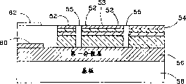
图4及5所示为该新发光二极管51的另一实施例,该新发光二极管并没有一隔开第一分散层及第二分散层的绝缘层。微发光二极管52是通过一互连栅格54的导电通路与相邻的微发光二极管连接,其中该通路的下面有半导体材料。每个栅格54中的开口55为一区域,其处的半导体材料在制造该发光二极管51时,从该发光二极管结构被蚀掉。该结构的剩余部份在该栅格54下为微发光二极管52,而在该些微发光二极管之间的栅格通路53下为半导体材料。微发光二极管及在该通路下的材料包含一由两个相反掺杂层包围的活性层,而整个结构则在一第一分散层56及一基板58之上形成。
一沉积在第一分散层上的第一接触点60将电流施加到微发光二极管的下层,而一包含在电流分散栅格上的第二接触点62将电流分散到微发光二极管的上层。当施加一偏压到该接触点60及62时,电流被施加到该微发光二极管及在导电通路下的的半导体材料,使它们全部发光。光从该些通路下的微发光二极管材料的侧面逸出,避免了全内反射。因此本技术可以通用于在任何基板上的任何发光二极管结构以及可以用标准处理技术来实现。
要制造发光二极管51首先要在基板58上沉积第一分散层56,然后再形成一连续的发光二极管结构,其将电流分散层56覆盖。栅格54沉积在该发光二极管结构上,而该发光二极管结构在该栅格开口中可见到的部份可以不同的方法来蚀除,例如湿式化学蚀刻、反应离子蚀刻(RIE)、离子研磨、或任何其它用于移除半导体材料的技术。部份的发光二极管结构也被蚀刻以提供一接触点60区域,使接触点60及62在其上沉积。栅格54可以任何导电材料来制造,包括但不限于金属、半金属、半导体、或其组合。微发光二极管最好基于GaN,而每个微发光二极管的上层55为一p-型AlGaInN或其任何合金,而栅格54最好以一薄金属来制造,例如Ni、Pd、Au、Pt或其任何组合。
图4中的虚线示出微发光二极管其中之一以及该微发光二极管周围的区域,在其处可包含LEEs以进一步加强光放出,以下将会充分地叙述。
图6及7所示为该新发光二极管的两个额外的实施例70和80,其具有不同的微发光二极管及栅格结构72及82,尽管还可用许多不同的结构。每一实施例具有一个别的下分散接触点73及83。在图6中,该互连的微发光二极管74通过不同的通路将电流交叉分散到每个微发光二极管。在每条通路下有半导体材料以使其与第一分散层隔离。栅格72提供呈正方阵列结构的开口以与光相互作用。
栅格54有一优于栅格72之处。在发光二极管70中,TIR光可沿栅格的许多的导电通路的其中之一反射以及可在不与该些微发光二极管的其中之一的表面相互作用下于该发光二极管之内反射。在该栅格中或在下层中的光耗将会造成某些TIR光在其逸出新发光二极管的最终边缘之前被吸收掉。栅格54将此问题减少,因为从微发光二极管发射的光在传播仅仅一短距离之后(最多为两个微发光二极管的长度)就到达一侧面,从而使逸出该装置的光增加。
在图7中,微发光二极管是随机性地成形以及具有随机的互连通路。此外,在该些通路下有半导体材料。该随机结构使TIR光在遇到其中一栅格开口中的其中一微发光二极管之前可供TIR光传播的通路数目降低。如上所述,在图6及7中环绕微发光二极管的虚线示出微发光二极管76及86和环绕在其周边的LEEs,以下将会充分地叙述。
开口尺寸及开口之间的距离最好在1到30μm之间,但可以较大或者较小。该开口的可以是非周期或周期结构,因为光与微发光二极管边缘的相互作用在本质上并不需要以上任一条件。在较佳实施例中,在一p-型AlGaInN层上的栅格开口的宽度在1微米到20微米之间,微发光二极管的宽度则在1微米到30微米之间。
先前的三个实施例全部都可与在微发光二极管之间的LEEs结合来进一步增加光发射。该LEEs既可在微发光二极管的侧面上,又可在第一分散层的表面形成,或者,在那些不具有第一分散层的实施例中则可在导电基板上形成。
尽管可以使用其它的LEEs形状以及本发明的保护范围也不限于所示的形状,图8仍示出了若干可供选择的LEEs形状,该些形状包含在本发明的实施例中。LEEs82、84、86具有曲面,而LEEs 88、90、92、94则具有分段的线性表面。另外,该LEE可为一随机糙面层,其可做为一光弥散器。
LEEs可用标准蚀刻技术来形成,例如湿式化学蚀刻,RIE,或离子研磨。在该较佳实施例中,LEEs是通过使用一商用的做为一烧蚀蚀刻掩模的聚合物来形成的(例如一紫外线或电子束敏感光阻)。此聚合物首先被沉积,并形成为类似方边的结构。该聚合物会加热到一个温度,并如玻璃般重熔以致该聚合物的边缘形成一逐渐线性或弯曲的形状。该聚合物厚度、结构形状、加热温度及加热时间将决定该边缘形状。该结构可以以RIE转换到基于AlGaInN的微发光二极管。用此方法可轻易地制造线性及曲形的LEEs,而通过使用多个蚀刻掩模可轻易地构造分段式线性LEEs。
用来形成LEEs的第二种技术是使用负极性UV可曝光光阻。首先,使该光阻持续曝光一特定的曝光时间,并将其加工以产生一负极性。然后使该光阻显影以在其截面产生一削底的弯曲或线性形状。然后此结构可经由一干式蚀刻技术转换到半导体材料。对这两个实施例而言,干式蚀刻的环境也会影响半导体材料中透镜的最终形状。
图9-15所示为新发光二极管的实施例,其中LEEs以各种各样的方式与微发光二极管阵列结合以加强光放出。这些实施例说明根据本发明的LEEs的一些可行的使用方式,而本发明的保护范围并受不限于所述的实施例。
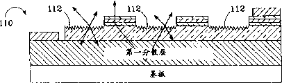
图9所示为一类似于图4及5中的发光二极管51的新的发光二极管100,但其在微发光二极管104之间具有LEEs 101、102、103。该些LEEs 101、102、103使被导向穿过一微发光二极管的侧面的光可从该LEEs反射出去,并将光从该基板重新导向到一外壳中。从基板108及第一分散层106之间的介面反射出去的光透过TIR还可以与LEEs 101、102、103相互作用而逸出到该外壳中以提供一较强的光输出。在图8中所述的LEEs可以沉积在新发光二极管上,或是加工到新发光二极管中。如上所述,LEE的厚度也可改变,较佳的厚度在0.5μm到10μm的范围内。
图10所示为一新发光二极管110,其类似于图9的发光二极管100,但其在该微发光二极管113之间具有随机的糙面的弥散LEE 112。光与粗糙层的相互作用使TIR光能以小于其临界角之下抵达表面,并且在被吸收之前逸出。在该较佳实施例中,通过使用聚苯乙烯或硅微球体作为一蚀刻掩模将微量粗糙度转到半导体中来形成该粗糙面。随机粗糙度的厚度及宽度可小于20nm,或多到500nm,较佳的尺寸大约为发光二极管所产生的光的波长。
图11所示为一新发光二极管120,其类似于图10的发光二极管110,但其包括一在该微发光二极管中的电流阻隔层。该阻隔层122将电流导引到弥散LEE 124之下,增加了光与LEE相互作用及逸出的机会。
作为在微发光二极管之间形成LEEs的选择,可使LEEs直接形成于微发光二极管的侧面上。图12所示为一新发光二极管130,其类似于图9、10及11的发光二极管,但其具有直接形成于每个微发光二极管的侧面上的不同的LEEs 131-133。该LEEs可利用如上所述的相同的方法来形成。向微发光二极管侧面传播的光线被改向以使光线从基板134的其中一面通过第一分散层135或微发光二极管132逸出。由于在微发光二极管边上的该些LEEs,还使自基板134反射回来的光的逸出机会增加。
图13所示为一新发光二极管140,其有形成于微发光二极管144的侧面上的曲面的LEEs 142。该曲面LEE 142有额外的益处,其使发光二极管的光聚焦到一更明确的方向。LEEs 142的厚度及宽度可以随着任何一个LEE的较佳厚度而改变,该较佳厚度为0.1μm到50μm。
图14及15所示为两个额外的实施例。图14所示为一新发光二极管150,其在微发光二极管154的侧面上有一组合曲面的LEEs 152以及在该微发光二极管154之间有完全曲面的LEEs 156。该些LEEs共同作用,使光线折射及反射穿过基板逸出该发光二极管的外壳来加强光放出。
图15所示为新的发光二极管160,其使用类似于图3所示的实施例的具体的倒装式安装。其在微发光二极管164的侧面上有曲面LEEs 162。该第二分散层164为反光的以及该基板166为主要的发射表面。LEEs 162及第二分散层164的部份共同作用,使光线折射及反射穿过基板逸出发光二极管的外壳来加强光放出。
虽然本发明已根据其若干较佳的配置作出了相当详细的叙述,其它的变型也是可能的。举例来说,在微发光二极管阵列中的微发光二极管的下层可以连接。所使用的光放出结构也可以作许多不同的组合以及有许多不同的形状及尺寸。同时,所述的发光二极管结构可具有多于一个夹在相反掺杂层之间的活性层。因此,本发明的权利要求书的精神及保护范围并不受限于其所述的较佳实施例。
Claims (10)
1.一种具有加强光放出的发光二极管,其特征在于其包括:
一导电的第一分散层(20);
多个微发光二极管(12)分别地沉积在所述第一分散层(20)的一表面上,每个所述微发光二极管皆包含:
一p-型层(16);
一n-型层(18);
一活性层(14),其夹在所述p-型与n-型层(16,18)之间,其中所述p-型或n-型层为一上层,而另外一层则为下层,来自所述第一分散层(20)的电流分散到所述下层;
一第二分散层(24),其在所述微发光二极管(12)之上,来自所述第二分散层(24)的电流分散到所述上层,向所述第一及第二分散层(20,24)施加一偏压会使所述微发光二极管(12)发光。
2.根据权利要求1所述的发光二极管,其特征在于其进一步包含一基板(28),该基板与所述第一分散层(20)的与所述微发光二极管(12)相反的表面邻接。
3.根据权利要求1所述的发光二极管,其特征在于其进一步包含一绝缘层(23),该绝缘层覆盖所述微发光二极管(12)以及位于所述微发光二极管(12)之间的所述第一分散层(20)的表面,所述绝缘层(23)沉积在所述第二分散层(24)和所述微发光二极管(12)之间。
4.根据权利要求3所述的发光二极管,其特征在于所述绝缘层(23)在每个所述微发光二极管(12)上均设有空穴,所述第二分散层(24)藉由该空穴与每个所述微发光二极管(12)接触。
5.根据权利要求4所述的发光二极管,其特征在于所述第二分散层(24)为一互连的电流分散栅格,其具有多个互连的导电通路,每个所述微发光二极管(12)其上均具有一个或多个导电通路,并透过所述空穴与所述上层接触。
6.根据权利要求1所述的发光二极管,其特征在于其进一步包含光放出组件(82,84,86,88,90,92,94),其与所述微发光二极管(12)结合以与自微发光二极管(12)逸出的光相互作用,从而进一步加强自所述发光二极管放出的光。
7.根据权利要求6所述的发光二极管,其特征在于所述光放出组件(101,102,103)系沉积在所述第一分散层(106)的表面上以及在所述微发光二极管(104)之间。
8.根据权利要求4所述的发光二极管,其特征在于所述第二分散层(42)为一反光金属层,其沉积在该微发光二极管(32)之上,所述发光二极管进一步包含基板(36),该基板与所述第一分散层(34)的与所述微发光二极管(32)相反的表面邻接,及一与所述金属层(42)固接的次固定层(46),所述发光二极管的所述基板(36)成为主要的发光表面。
9.根据权利要求8所述的发光二极管,其特征在于其进一步包含一导电指形件(49),该指形件位于所述次固定层(46)和所述第一分散层(34)之间,一在所述次固定层(46)上的第一接触点(50)与所述导电指形件(49)连接,以及一在所述次固定层(46)上的第二接触点(44)与所述金属层(48)连接,所述微发光二极管(32)在一偏压被施加于所述接触点(44,50)时,即发光。
10.一种发光二极管,其特征在于其包括:
一第一分散层(56);
一微发光二极管(52)阵列,其沉积在所述第一分散层(56)上,一施加于所述第一分散层(56)的电流分散到所述微发光二极管(52);
一互连的电流分散栅格(54)沉积在所述微发光二极管(52)之上,所述栅格在所述微发光二极管(52)之间设有导电通路(53),一施加于所述栅格(54)的电流分散到所述微发光二极管(52);
半导体材料,其位于微发光二极管(52)之间的所述导电通路(53)之下,所述半导体材料使所述第一分散层(56)与所述导电通路(53)电绝缘;
分别位于所述第一及第二分散层(56,54)上的第一及第二接触点(60,62),向所述接触点(60,62)施加一偏压会使所述微发光二极管(52)阵列发光。
Applications Claiming Priority (4)
| Application Number | Priority Date | Filing Date | Title |
|---|---|---|---|
| US16881799P | 1999-12-03 | 1999-12-03 | |
| US60/168,817 | 1999-12-03 | ||
| US09/713,576 | 2000-11-14 | ||
| US09/713,576 US6410942B1 (en) | 1999-12-03 | 2000-11-14 | Enhanced light extraction through the use of micro-LED arrays |
Publications (2)
| Publication Number | Publication Date |
|---|---|
| CN1402880A CN1402880A (zh) | 2003-03-12 |
| CN1229871C true CN1229871C (zh) | 2005-11-30 |
Family
ID=26864480
Family Applications (1)
| Application Number | Title | Priority Date | Filing Date |
|---|---|---|---|
| CNB008166013A Expired - Lifetime CN1229871C (zh) | 1999-12-03 | 2000-11-20 | 加强光放出的微发光二极管阵列 |
Country Status (9)
| Country | Link |
|---|---|
| US (1) | US6410942B1 (zh) |
| EP (3) | EP2325903B1 (zh) |
| JP (1) | JP5511114B2 (zh) |
| KR (1) | KR100731673B1 (zh) |
| CN (1) | CN1229871C (zh) |
| AU (1) | AU1790501A (zh) |
| CA (1) | CA2393007C (zh) |
| HK (1) | HK1048707A1 (zh) |
| WO (1) | WO2001041219A1 (zh) |
Cited By (1)
| Publication number | Priority date | Publication date | Assignee | Title |
|---|---|---|---|---|
| CN103312412A (zh) * | 2012-03-06 | 2013-09-18 | 财团法人工业技术研究院 | 可见光通信收发器与系统 |
Families Citing this family (356)
| Publication number | Priority date | Publication date | Assignee | Title |
|---|---|---|---|---|
| CA2393081C (en) * | 1999-12-03 | 2011-10-11 | Cree Lighting Company | Enhanced light extraction in leds through the use of internal and external optical elements |
| US7547921B2 (en) * | 2000-08-08 | 2009-06-16 | Osram Opto Semiconductors Gmbh | Semiconductor chip for optoelectronics |
| US20020017652A1 (en) * | 2000-08-08 | 2002-02-14 | Stefan Illek | Semiconductor chip for optoelectronics |
| JP2002141556A (ja) | 2000-09-12 | 2002-05-17 | Lumileds Lighting Us Llc | 改良された光抽出効果を有する発光ダイオード |
| US7064355B2 (en) | 2000-09-12 | 2006-06-20 | Lumileds Lighting U.S., Llc | Light emitting diodes with improved light extraction efficiency |
| US7053419B1 (en) | 2000-09-12 | 2006-05-30 | Lumileds Lighting U.S., Llc | Light emitting diodes with improved light extraction efficiency |
| JP2002198560A (ja) * | 2000-12-26 | 2002-07-12 | Sharp Corp | 半導体発光素子およびその製造方法 |
| US6791119B2 (en) * | 2001-02-01 | 2004-09-14 | Cree, Inc. | Light emitting diodes including modifications for light extraction |
| JP4724924B2 (ja) * | 2001-02-08 | 2011-07-13 | ソニー株式会社 | 表示装置の製造方法 |
| US6746889B1 (en) * | 2001-03-27 | 2004-06-08 | Emcore Corporation | Optoelectronic device with improved light extraction |
| JP2002344011A (ja) * | 2001-05-15 | 2002-11-29 | Sony Corp | 表示素子及びこれを用いた表示装置 |
| US6897704B2 (en) * | 2001-05-25 | 2005-05-24 | Thunder Creative Technologies, Inc. | Electronic isolator |
| TW583348B (en) * | 2001-06-19 | 2004-04-11 | Phoenix Prec Technology Corp | A method for electroplating Ni/Au layer substrate without using electroplating wire |
| JP4055503B2 (ja) * | 2001-07-24 | 2008-03-05 | 日亜化学工業株式会社 | 半導体発光素子 |
| JP2005503043A (ja) | 2001-08-30 | 2005-01-27 | オスラム オプト セミコンダクターズ ゲゼルシャフト ミット ベシュレンクテル ハフツング | エレクトロルミネセンス体 |
| TW523939B (en) * | 2001-11-07 | 2003-03-11 | Nat Univ Chung Hsing | High-efficient light emitting diode and its manufacturing method |
| US6881983B2 (en) * | 2002-02-25 | 2005-04-19 | Kopin Corporation | Efficient light emitting diodes and lasers |
| JP3776824B2 (ja) | 2002-04-05 | 2006-05-17 | 株式会社東芝 | 半導体発光素子およびその製造方法 |
| US20030189215A1 (en) | 2002-04-09 | 2003-10-09 | Jong-Lam Lee | Method of fabricating vertical structure leds |
| JP4585014B2 (ja) * | 2002-04-12 | 2010-11-24 | ソウル セミコンダクター カンパニー リミテッド | 発光装置 |
| US20060175625A1 (en) * | 2002-05-28 | 2006-08-10 | Ryoji Yokotani | Light emitting element, lighting device and surface emission illuminating device using it |
| US6841802B2 (en) * | 2002-06-26 | 2005-01-11 | Oriol, Inc. | Thin film light emitting diode |
| US6955985B2 (en) * | 2002-06-28 | 2005-10-18 | Kopin Corporation | Domain epitaxy for thin film growth |
| DE10234977A1 (de) * | 2002-07-31 | 2004-02-12 | Osram Opto Semiconductors Gmbh | Strahlungsemittierendes Dünnschicht-Halbleiterbauelement auf GaN-Basis |
| KR101052139B1 (ko) * | 2002-08-01 | 2011-07-26 | 니치아 카가쿠 고교 가부시키가이샤 | 반도체 발광 소자 및 그 제조 방법과 그것을 이용한 발광장치 |
| KR20040013998A (ko) * | 2002-08-09 | 2004-02-14 | 엘지전자 주식회사 | 표면 방출형 발광 다이오드의 제조방법 |
| DE60336252D1 (de) * | 2002-08-29 | 2011-04-14 | Seoul Semiconductor Co Ltd | Lichtemittierendes bauelement mit lichtemittierenden dioden |
| JP3956918B2 (ja) | 2002-10-03 | 2007-08-08 | 日亜化学工業株式会社 | 発光ダイオード |
| US7071494B2 (en) * | 2002-12-11 | 2006-07-04 | Lumileds Lighting U.S. Llc | Light emitting device with enhanced optical scattering |
| WO2004061980A1 (de) * | 2002-12-30 | 2004-07-22 | Osram Opto Semiconductors Gmbh | Verfahren zum aufrauhen einer oberfläche eines körpers und optoelektronisches bauelement |
| US7042020B2 (en) * | 2003-02-14 | 2006-05-09 | Cree, Inc. | Light emitting device incorporating a luminescent material |
| KR100964399B1 (ko) * | 2003-03-08 | 2010-06-17 | 삼성전자주식회사 | 반도체 레이저 다이오드 및 이를 채용한 반도체 레이저다이오드 조립체 |
| US7074631B2 (en) * | 2003-04-15 | 2006-07-11 | Luminus Devices, Inc. | Light emitting device methods |
| US7211831B2 (en) * | 2003-04-15 | 2007-05-01 | Luminus Devices, Inc. | Light emitting device with patterned surfaces |
| US7105861B2 (en) * | 2003-04-15 | 2006-09-12 | Luminus Devices, Inc. | Electronic device contact structures |
| US6831302B2 (en) * | 2003-04-15 | 2004-12-14 | Luminus Devices, Inc. | Light emitting devices with improved extraction efficiency |
| US20040259279A1 (en) * | 2003-04-15 | 2004-12-23 | Erchak Alexei A. | Light emitting device methods |
| US7083993B2 (en) * | 2003-04-15 | 2006-08-01 | Luminus Devices, Inc. | Methods of making multi-layer light emitting devices |
| US7098589B2 (en) | 2003-04-15 | 2006-08-29 | Luminus Devices, Inc. | Light emitting devices with high light collimation |
| US7166871B2 (en) * | 2003-04-15 | 2007-01-23 | Luminus Devices, Inc. | Light emitting systems |
| US7274043B2 (en) * | 2003-04-15 | 2007-09-25 | Luminus Devices, Inc. | Light emitting diode systems |
| US7084434B2 (en) * | 2003-04-15 | 2006-08-01 | Luminus Devices, Inc. | Uniform color phosphor-coated light-emitting diode |
| US7667238B2 (en) * | 2003-04-15 | 2010-02-23 | Luminus Devices, Inc. | Light emitting devices for liquid crystal displays |
| US7262550B2 (en) * | 2003-04-15 | 2007-08-28 | Luminus Devices, Inc. | Light emitting diode utilizing a physical pattern |
| US7521854B2 (en) * | 2003-04-15 | 2009-04-21 | Luminus Devices, Inc. | Patterned light emitting devices and extraction efficiencies related to the same |
| EP2264798B1 (en) * | 2003-04-30 | 2020-10-14 | Cree, Inc. | High powered light emitter packages with compact optics |
| US7005679B2 (en) | 2003-05-01 | 2006-02-28 | Cree, Inc. | Multiple component solid state white light |
| IE20040308A1 (en) * | 2003-05-02 | 2004-11-17 | Univ College Cork Nat Univ Ie | Light emitting diodes and the manufacture thereof |
| US6885034B1 (en) | 2003-05-09 | 2005-04-26 | Winston Vaughan Schoenfeld | Light emitting diode having multiple pits |
| US7122841B2 (en) | 2003-06-04 | 2006-10-17 | Kopin Corporation | Bonding pad for gallium nitride-based light-emitting devices |
| US20050000913A1 (en) * | 2003-07-03 | 2005-01-06 | Mark Betterly | Fluid treatment system |
| US7009213B2 (en) | 2003-07-31 | 2006-03-07 | Lumileds Lighting U.S., Llc | Light emitting devices with improved light extraction efficiency |
| US7595511B2 (en) * | 2003-08-08 | 2009-09-29 | Sang-Kyu Kang | Nitride micro light emitting diode with high brightness and method of manufacturing the same |
| WO2005018008A1 (ja) * | 2003-08-19 | 2005-02-24 | Nichia Corporation | 半導体素子 |
| US7344903B2 (en) * | 2003-09-17 | 2008-03-18 | Luminus Devices, Inc. | Light emitting device processes |
| US7341880B2 (en) * | 2003-09-17 | 2008-03-11 | Luminus Devices, Inc. | Light emitting device processes |
| US7915085B2 (en) * | 2003-09-18 | 2011-03-29 | Cree, Inc. | Molded chip fabrication method |
| US8604497B2 (en) * | 2003-09-26 | 2013-12-10 | Osram Opto Semiconductors Gmbh | Radiation-emitting thin-film semiconductor chip |
| WO2005064666A1 (en) | 2003-12-09 | 2005-07-14 | The Regents Of The University Of California | Highly efficient gallium nitride based light emitting diodes via surface roughening |
| US7450311B2 (en) | 2003-12-12 | 2008-11-11 | Luminus Devices, Inc. | Optical display systems and methods |
| JP2005191099A (ja) * | 2003-12-24 | 2005-07-14 | ▲さん▼圓光電股▲ふん▼有限公司 | 発光ダイオード装置 |
| US20050179046A1 (en) * | 2004-02-13 | 2005-08-18 | Kopin Corporation | P-type electrodes in gallium nitride-based light-emitting devices |
| US20050179042A1 (en) * | 2004-02-13 | 2005-08-18 | Kopin Corporation | Monolithic integration and enhanced light extraction in gallium nitride-based light-emitting devices |
| TWM271252U (en) * | 2004-12-14 | 2005-07-21 | Niching Ind Corp | Package structure of light-emitting device |
| JP2005259891A (ja) * | 2004-03-10 | 2005-09-22 | Toyoda Gosei Co Ltd | 発光装置 |
| US7202141B2 (en) * | 2004-03-29 | 2007-04-10 | J.P. Sercel Associates, Inc. | Method of separating layers of material |
| US7419912B2 (en) * | 2004-04-01 | 2008-09-02 | Cree, Inc. | Laser patterning of light emitting devices |
| US7064356B2 (en) * | 2004-04-16 | 2006-06-20 | Gelcore, Llc | Flip chip light emitting diode with micromesas and a conductive mesh |
| US7795623B2 (en) * | 2004-06-30 | 2010-09-14 | Cree, Inc. | Light emitting devices having current reducing structures and methods of forming light emitting devices having current reducing structures |
| US7534633B2 (en) * | 2004-07-02 | 2009-05-19 | Cree, Inc. | LED with substrate modifications for enhanced light extraction and method of making same |
| US20090023239A1 (en) * | 2004-07-22 | 2009-01-22 | Luminus Devices, Inc. | Light emitting device processes |
| US20060038188A1 (en) * | 2004-08-20 | 2006-02-23 | Erchak Alexei A | Light emitting diode systems |
| US20060049418A1 (en) * | 2004-09-03 | 2006-03-09 | Tzi-Chi Wen | Epitaxial structure and fabrication method of nitride semiconductor device |
| US8174037B2 (en) * | 2004-09-22 | 2012-05-08 | Cree, Inc. | High efficiency group III nitride LED with lenticular surface |
| US7259402B2 (en) * | 2004-09-22 | 2007-08-21 | Cree, Inc. | High efficiency group III nitride-silicon carbide light emitting diode |
| US7737459B2 (en) * | 2004-09-22 | 2010-06-15 | Cree, Inc. | High output group III nitride light emitting diodes |
| US8513686B2 (en) * | 2004-09-22 | 2013-08-20 | Cree, Inc. | High output small area group III nitride LEDs |
| US7352006B2 (en) * | 2004-09-28 | 2008-04-01 | Goldeneye, Inc. | Light emitting diodes exhibiting both high reflectivity and high light extraction |
| US7329982B2 (en) | 2004-10-29 | 2008-02-12 | 3M Innovative Properties Company | LED package with non-bonded optical element |
| US7404756B2 (en) | 2004-10-29 | 2008-07-29 | 3M Innovative Properties Company | Process for manufacturing optical and semiconductor elements |
| US20060091411A1 (en) | 2004-10-29 | 2006-05-04 | Ouderkirk Andrew J | High brightness LED package |
| US7462502B2 (en) | 2004-11-12 | 2008-12-09 | Philips Lumileds Lighting Company, Llc | Color control by alteration of wavelength converting element |
| US7419839B2 (en) | 2004-11-12 | 2008-09-02 | Philips Lumileds Lighting Company, Llc | Bonding an optical element to a light emitting device |
| JP2006147679A (ja) * | 2004-11-17 | 2006-06-08 | Sony Corp | 集積型発光ダイオード、集積型発光ダイオードの製造方法、発光ダイオードディスプレイおよび発光ダイオード照明装置 |
| US7304363B1 (en) | 2004-11-26 | 2007-12-04 | United States Of America As Represented By The Secretary Of The Army | Interacting current spreader and junction extender to increase the voltage blocked in the off state of a high power semiconductor device |
| US20060124943A1 (en) * | 2004-12-14 | 2006-06-15 | Elite Optoelectronics Inc. | Large-sized light-emitting diodes with improved light extraction efficiency |
| US8288942B2 (en) | 2004-12-28 | 2012-10-16 | Cree, Inc. | High efficacy white LED |
| KR101138974B1 (ko) * | 2005-01-07 | 2012-04-25 | 서울옵토디바이스주식회사 | 발광 소자 및 이의 제조 방법 |
| JP4687109B2 (ja) * | 2005-01-07 | 2011-05-25 | ソニー株式会社 | 集積型発光ダイオードの製造方法 |
| US7524686B2 (en) * | 2005-01-11 | 2009-04-28 | Semileds Corporation | Method of making light emitting diodes (LEDs) with improved light extraction by roughening |
| US20060154393A1 (en) * | 2005-01-11 | 2006-07-13 | Doan Trung T | Systems and methods for removing operating heat from a light emitting diode |
| US7186580B2 (en) * | 2005-01-11 | 2007-03-06 | Semileds Corporation | Light emitting diodes (LEDs) with improved light extraction by roughening |
| US20060151801A1 (en) * | 2005-01-11 | 2006-07-13 | Doan Trung T | Light emitting diode with thermo-electric cooler |
| US7692207B2 (en) * | 2005-01-21 | 2010-04-06 | Luminus Devices, Inc. | Packaging designs for LEDs |
| US7170100B2 (en) | 2005-01-21 | 2007-01-30 | Luminus Devices, Inc. | Packaging designs for LEDs |
| US7335920B2 (en) * | 2005-01-24 | 2008-02-26 | Cree, Inc. | LED with current confinement structure and surface roughening |
| KR101138944B1 (ko) * | 2005-01-26 | 2012-04-25 | 서울옵토디바이스주식회사 | 직렬 연결된 복수개의 발광셀들을 갖는 발광 소자 및그것을 제조하는 방법 |
| US7535028B2 (en) * | 2005-02-03 | 2009-05-19 | Ac Led Lighting, L.Lc. | Micro-LED based high voltage AC/DC indicator lamp |
| JP2006261659A (ja) * | 2005-02-18 | 2006-09-28 | Sumitomo Chemical Co Ltd | 半導体発光素子の製造方法 |
| US7932111B2 (en) | 2005-02-23 | 2011-04-26 | Cree, Inc. | Substrate removal process for high light extraction LEDs |
| US20070045640A1 (en) | 2005-08-23 | 2007-03-01 | Erchak Alexei A | Light emitting devices for liquid crystal displays |
| US20060204865A1 (en) * | 2005-03-08 | 2006-09-14 | Luminus Devices, Inc. | Patterned light-emitting devices |
| US8163575B2 (en) * | 2005-06-17 | 2012-04-24 | Philips Lumileds Lighting Company Llc | Grown photonic crystals in semiconductor light emitting devices |
| KR100599012B1 (ko) | 2005-06-29 | 2006-07-12 | 서울옵토디바이스주식회사 | 열전도성 기판을 갖는 발광 다이오드 및 그것을 제조하는방법 |
| US20090179211A1 (en) * | 2005-07-14 | 2009-07-16 | Tae-Kyung Yoo | Light emitting device |
| US20070018182A1 (en) * | 2005-07-20 | 2007-01-25 | Goldeneye, Inc. | Light emitting diodes with improved light extraction and reflectivity |
| US8674375B2 (en) * | 2005-07-21 | 2014-03-18 | Cree, Inc. | Roughened high refractive index layer/LED for high light extraction |
| US20070085098A1 (en) * | 2005-10-17 | 2007-04-19 | Luminus Devices, Inc. | Patterned devices and related methods |
| US7348603B2 (en) * | 2005-10-17 | 2008-03-25 | Luminus Devices, Inc. | Anisotropic collimation devices and related methods |
| US7388233B2 (en) * | 2005-10-17 | 2008-06-17 | Luminus Devices, Inc. | Patchwork patterned devices and related methods |
| US7391059B2 (en) | 2005-10-17 | 2008-06-24 | Luminus Devices, Inc. | Isotropic collimation devices and related methods |
| US20080099777A1 (en) * | 2005-10-19 | 2008-05-01 | Luminus Devices, Inc. | Light-emitting devices and related systems |
| KR100779078B1 (ko) * | 2005-12-09 | 2007-11-27 | 한국전자통신연구원 | 빛의 방출 효율을 향상시킬 수 있는 실리콘 발광 소자 및그 제조방법 |
| JP4908837B2 (ja) * | 2005-12-13 | 2012-04-04 | キヤノン株式会社 | 発光素子アレイ及び画像形成装置 |
| BRPI0620397A2 (pt) | 2005-12-22 | 2011-11-16 | Cree Led Lighting Solutions | dispositivo de iluminação |
| US7772604B2 (en) | 2006-01-05 | 2010-08-10 | Illumitex | Separate optical device for directing light from an LED |
| JP2007214260A (ja) * | 2006-02-08 | 2007-08-23 | Matsushita Electric Ind Co Ltd | 半導体発光素子およびその製造方法 |
| KR20070088145A (ko) * | 2006-02-24 | 2007-08-29 | 엘지전자 주식회사 | 발광 다이오드 및 그 제조방법 |
| JP2009538536A (ja) | 2006-05-26 | 2009-11-05 | クリー エル イー ディー ライティング ソリューションズ インコーポレイテッド | 固体発光デバイス、および、それを製造する方法 |
| US8596819B2 (en) | 2006-05-31 | 2013-12-03 | Cree, Inc. | Lighting device and method of lighting |
| KR100759896B1 (ko) * | 2006-06-15 | 2007-09-18 | 삼성전자주식회사 | 적어도 하나의 발광소자가 장착된 백라이트 모듈 및 그제작 방법 |
| US7674639B2 (en) * | 2006-08-14 | 2010-03-09 | Bridgelux, Inc | GaN based LED with etched exposed surface for improved light extraction efficiency and method for making the same |
| WO2008024385A2 (en) * | 2006-08-23 | 2008-02-28 | Cree Led Lighting Solutions, Inc. | Lighting device and lighting method |
| US20100224890A1 (en) * | 2006-09-18 | 2010-09-09 | Cree, Inc. | Light emitting diode chip with electrical insulation element |
| JP2010506402A (ja) * | 2006-10-02 | 2010-02-25 | イルミテックス, インコーポレイテッド | Ledのシステムおよび方法 |
| US20090275157A1 (en) * | 2006-10-02 | 2009-11-05 | Illumitex, Inc. | Optical device shaping |
| US20080087875A1 (en) * | 2006-10-11 | 2008-04-17 | Feng-Hsu Fan | Protection for the epitaxial structure of metal devices |
| US9318327B2 (en) | 2006-11-28 | 2016-04-19 | Cree, Inc. | Semiconductor devices having low threading dislocations and improved light extraction and methods of making the same |
| WO2008070604A1 (en) * | 2006-12-04 | 2008-06-12 | Cree Led Lighting Solutions, Inc. | Lighting device and lighting method |
| WO2008070607A1 (en) | 2006-12-04 | 2008-06-12 | Cree Led Lighting Solutions, Inc. | Lighting assembly and lighting method |
| US8110838B2 (en) * | 2006-12-08 | 2012-02-07 | Luminus Devices, Inc. | Spatial localization of light-generating portions in LEDs |
| CN101652861B (zh) * | 2007-01-22 | 2013-01-23 | 科锐公司 | 容错发光体、包含容错发光体的系统以及制造容错发光体的方法 |
| EP3223313B1 (en) * | 2007-01-22 | 2021-04-14 | Cree, Inc. | Monolithic light emitter having multiple light emitting sub-devices |
| US8110425B2 (en) | 2007-03-20 | 2012-02-07 | Luminus Devices, Inc. | Laser liftoff structure and related methods |
| KR100849826B1 (ko) | 2007-03-29 | 2008-07-31 | 삼성전기주식회사 | 발광소자 및 이를 포함하는 패키지 |
| CN101743488B (zh) * | 2007-07-17 | 2014-02-26 | 科锐公司 | 具有内部光学特性结构的光学元件及其制造方法 |
| US8617997B2 (en) * | 2007-08-21 | 2013-12-31 | Cree, Inc. | Selective wet etching of gold-tin based solder |
| US11114594B2 (en) * | 2007-08-24 | 2021-09-07 | Creeled, Inc. | Light emitting device packages using light scattering particles of different size |
| US8368100B2 (en) | 2007-11-14 | 2013-02-05 | Cree, Inc. | Semiconductor light emitting diodes having reflective structures and methods of fabricating same |
| US9431589B2 (en) * | 2007-12-14 | 2016-08-30 | Cree, Inc. | Textured encapsulant surface in LED packages |
| DE102008019902A1 (de) * | 2007-12-21 | 2009-06-25 | Osram Opto Semiconductors Gmbh | Optoelektronisches Bauelement und Herstellungsverfahren für ein optoelektronisches Bauelement |
| DE102008003182A1 (de) * | 2008-01-04 | 2009-07-09 | Osram Opto Semiconductors Gmbh | Optoelektronisches Bauelement |
| US7829358B2 (en) | 2008-02-08 | 2010-11-09 | Illumitex, Inc. | System and method for emitter layer shaping |
| JP5094535B2 (ja) * | 2008-05-07 | 2012-12-12 | 富士フイルム株式会社 | 凹部形成方法、凹凸製品の製造方法、発光素子の製造方法および光学素子の製造方法 |
| EP2303039A4 (en) * | 2008-06-11 | 2011-08-31 | Susanne Gardner | BEVERAGES COMPOSED FROM WINE STUFFS |
| US7939839B2 (en) * | 2008-09-11 | 2011-05-10 | Bridgelux, Inc. | Series connected segmented LED |
| US7825427B2 (en) * | 2008-09-12 | 2010-11-02 | Bridgelux, Inc. | Method and apparatus for generating phosphor film with textured surface |
| US9051177B2 (en) * | 2008-10-27 | 2015-06-09 | The United States Of America As Represented By The Secretary Of The Army | Active optical limiting semiconductor device and method with active region transparent to light becoming opaque when not biased |
| TWI375338B (en) * | 2008-11-27 | 2012-10-21 | Epistar Corp | Opto-electronic device |
| TW201034256A (en) | 2008-12-11 | 2010-09-16 | Illumitex Inc | Systems and methods for packaging light-emitting diode devices |
| TWI418060B (zh) * | 2008-12-26 | 2013-12-01 | Lextar Electronics Corp | 發光二極體晶片的製造方法 |
| US7982409B2 (en) | 2009-02-26 | 2011-07-19 | Bridgelux, Inc. | Light sources utilizing segmented LEDs to compensate for manufacturing variations in the light output of individual segmented LEDs |
| KR101134810B1 (ko) | 2009-03-03 | 2012-04-13 | 엘지이노텍 주식회사 | 발광소자 및 그 제조방법 |
| JP5196403B2 (ja) * | 2009-03-23 | 2013-05-15 | 国立大学法人山口大学 | サファイア基板の製造方法、および半導体装置 |
| US8585253B2 (en) | 2009-08-20 | 2013-11-19 | Illumitex, Inc. | System and method for color mixing lens array |
| US8449128B2 (en) | 2009-08-20 | 2013-05-28 | Illumitex, Inc. | System and method for a lens and phosphor layer |
| KR20110043282A (ko) * | 2009-10-21 | 2011-04-27 | 엘지이노텍 주식회사 | 발광소자 및 그 제조방법 |
| KR101039931B1 (ko) * | 2009-10-21 | 2011-06-09 | 엘지이노텍 주식회사 | 발광 소자 및 그 제조방법 |
| US8783915B2 (en) | 2010-02-11 | 2014-07-22 | Bridgelux, Inc. | Surface-textured encapsulations for use with light emitting diodes |
| US8338317B2 (en) | 2011-04-06 | 2012-12-25 | Infineon Technologies Ag | Method for processing a semiconductor wafer or die, and particle deposition device |
| KR100999733B1 (ko) * | 2010-02-18 | 2010-12-08 | 엘지이노텍 주식회사 | 발광 소자, 발광 소자 제조방법 및 발광 소자 패키지 |
| KR101601624B1 (ko) * | 2010-02-19 | 2016-03-09 | 삼성전자주식회사 | 멀티셀 어레이를 갖는 반도체 발광장치, 발광모듈 및 조명장치 |
| TWI485884B (zh) * | 2010-03-30 | 2015-05-21 | Advanced Optoelectronic Tech | 發光二極體及其製作方法 |
| US8329482B2 (en) | 2010-04-30 | 2012-12-11 | Cree, Inc. | White-emitting LED chips and method for making same |
| KR20110132136A (ko) * | 2010-06-01 | 2011-12-07 | 삼성전자주식회사 | 연결 구조를 이용한 발광소자 및 그 제조 방법 |
| US8193546B2 (en) * | 2010-06-04 | 2012-06-05 | Pinecone Energies, Inc. | Light-emitting-diode array with polymer between light emitting devices |
| KR20180126634A (ko) * | 2010-07-26 | 2018-11-27 | 가부시키가이샤 한도오따이 에네루기 켄큐쇼 | 발광 디바이스 및 조명 디바이스 |
| US9070851B2 (en) | 2010-09-24 | 2015-06-30 | Seoul Semiconductor Co., Ltd. | Wafer-level light emitting diode package and method of fabricating the same |
| US9899329B2 (en) | 2010-11-23 | 2018-02-20 | X-Celeprint Limited | Interconnection structures and methods for transfer-printed integrated circuit elements with improved interconnection alignment tolerance |
| JP5589812B2 (ja) | 2010-12-06 | 2014-09-17 | 豊田合成株式会社 | 半導体発光素子 |
| US9166126B2 (en) | 2011-01-31 | 2015-10-20 | Cree, Inc. | Conformally coated light emitting devices and methods for providing the same |
| TWI467805B (zh) * | 2011-03-08 | 2015-01-01 | Opto Tech Corp | 具寬視角的發光二極體及其製造方法 |
| KR101106139B1 (ko) * | 2011-04-04 | 2012-01-20 | 서울옵토디바이스주식회사 | 확장된 금속 반사층을 갖는 플립 본딩형 발광다이오드 및 그 제조방법 |
| KR101115538B1 (ko) * | 2011-04-04 | 2012-02-28 | 서울옵토디바이스주식회사 | 발광소자와 그 제조방법 |
| US20120261686A1 (en) * | 2011-04-12 | 2012-10-18 | Lu Chi Wei | Light-emitting element and the manufacturing method thereof |
| KR101737981B1 (ko) | 2011-05-17 | 2017-05-22 | 한국전자통신연구원 | 마이크로 어레이 형태의 질화물 발광 소자 및 그 제조 방법 |
| US8934259B2 (en) | 2011-06-08 | 2015-01-13 | Semprius, Inc. | Substrates with transferable chiplets |
| KR101221336B1 (ko) * | 2011-07-12 | 2013-01-21 | 서울옵토디바이스주식회사 | 발광 소자 및 그것을 제조하는 방법 |
| US8957440B2 (en) | 2011-10-04 | 2015-02-17 | Cree, Inc. | Light emitting devices with low packaging factor |
| KR101901589B1 (ko) * | 2011-11-14 | 2018-09-27 | 엘지이노텍 주식회사 | 발광소자 |
| US8349116B1 (en) | 2011-11-18 | 2013-01-08 | LuxVue Technology Corporation | Micro device transfer head heater assembly and method of transferring a micro device |
| US8573469B2 (en) | 2011-11-18 | 2013-11-05 | LuxVue Technology Corporation | Method of forming a micro LED structure and array of micro LED structures with an electrically insulating layer |
| US8646505B2 (en) | 2011-11-18 | 2014-02-11 | LuxVue Technology Corporation | Micro device transfer head |
| US8809875B2 (en) | 2011-11-18 | 2014-08-19 | LuxVue Technology Corporation | Micro light emitting diode |
| KR101337613B1 (ko) * | 2011-12-06 | 2013-12-06 | 서울바이오시스 주식회사 | 발광소자와 그 제조방법 |
| WO2013116631A1 (en) | 2012-02-02 | 2013-08-08 | The Procter & Gamble Company | Light emitting laminate and method of making thereof |
| EP2812928B1 (en) | 2012-02-10 | 2019-04-17 | Facebook Technologies, LLC | Light emitting diode chip |
| GB201215632D0 (en) | 2012-09-03 | 2012-10-17 | Infiniled Ltd | Optical device |
| JP5462333B1 (ja) | 2012-09-21 | 2014-04-02 | 株式会社東芝 | 半導体発光素子及びその製造方法 |
| DE102012109460B4 (de) * | 2012-10-04 | 2024-03-07 | OSRAM Opto Semiconductors Gesellschaft mit beschränkter Haftung | Verfahren zur Herstellung eines Leuchtdioden-Displays und Leuchtdioden-Display |
| JP2016503516A (ja) * | 2012-11-15 | 2016-02-04 | 4233999 カナダ インコーポレイテッド | マイクロ発光ダイオードを使用する高速短距離光通信のための方法および装置 |
| US8558254B1 (en) | 2012-11-29 | 2013-10-15 | Hong Kong Applied Science and Technology Research Institute Company Limited | High reliability high voltage vertical LED arrays |
| US9105714B2 (en) * | 2012-12-11 | 2015-08-11 | LuxVue Technology Corporation | Stabilization structure including sacrificial release layer and staging bollards |
| US9166114B2 (en) * | 2012-12-11 | 2015-10-20 | LuxVue Technology Corporation | Stabilization structure including sacrificial release layer and staging cavity |
| US9306138B2 (en) * | 2013-04-08 | 2016-04-05 | Xiamen Sanan Optoelectronics Technology Co., Ltd. | Light emitting diode packaging structure |
| US20160329173A1 (en) | 2013-06-12 | 2016-11-10 | Rohinni, LLC | Keyboard backlighting with deposited light-generating sources |
| CN104241262B (zh) | 2013-06-14 | 2020-11-06 | 惠州科锐半导体照明有限公司 | 发光装置以及显示装置 |
| DE102013107967B4 (de) * | 2013-07-25 | 2021-05-06 | OSRAM Opto Semiconductors Gesellschaft mit beschränkter Haftung | Optoelektronischer Halbleiterchip, optoelektronisches Bauelement und Verfahren zur Herstellung einer Mehrzahl von optoelektronischen Halbleiterchips |
| JP2014064012A (ja) * | 2013-10-28 | 2014-04-10 | Toshiba Corp | 半導体発光素子及びその製造方法 |
| JP6684541B2 (ja) * | 2014-01-20 | 2020-04-22 | ローム株式会社 | 発光素子 |
| DE102014009677A1 (de) * | 2014-02-19 | 2015-08-20 | Pierre-Alain Cotte | Anzeigevorrichtung mit verbessertem Kontrast |
| US9105813B1 (en) * | 2014-05-30 | 2015-08-11 | Mikro Mesa Technology Co., Ltd. | Micro-light-emitting diode |
| US9231153B2 (en) * | 2014-05-30 | 2016-01-05 | Mikro Mesa Technology Co., Ltd. | Micro-light-emitting diode |
| CN113437206B (zh) | 2014-06-18 | 2024-03-08 | 艾克斯展示公司技术有限公司 | 微组装led显示器 |
| KR20170047324A (ko) | 2014-08-26 | 2017-05-04 | 엑스-셀레프린트 리미티드 | 마이크로 어셈블링된 하이브리드 디스플레이들 및 조명 엘리먼트들 |
| US9818725B2 (en) | 2015-06-01 | 2017-11-14 | X-Celeprint Limited | Inorganic-light-emitter display with integrated black matrix |
| US9799719B2 (en) | 2014-09-25 | 2017-10-24 | X-Celeprint Limited | Active-matrix touchscreen |
| US9991163B2 (en) | 2014-09-25 | 2018-06-05 | X-Celeprint Limited | Small-aperture-ratio display with electrical component |
| US9799261B2 (en) | 2014-09-25 | 2017-10-24 | X-Celeprint Limited | Self-compensating circuit for faulty display pixels |
| US9433050B2 (en) * | 2014-10-08 | 2016-08-30 | Mikro Mesa Technology Co., Ltd. | Micro-light-emitting diode |
| US20230261153A9 (en) * | 2014-10-31 | 2023-08-17 | eLux Inc. | Encapsulated Light Emitting Diodes for Selective Fluidic Assembly |
| US10516084B2 (en) | 2014-10-31 | 2019-12-24 | eLux, Inc. | Encapsulated fluid assembly emissive elements |
| GB201420452D0 (en) * | 2014-11-18 | 2014-12-31 | Mled Ltd | Integrated colour led micro-display |
| USD826871S1 (en) | 2014-12-11 | 2018-08-28 | Cree, Inc. | Light emitting diode device |
| KR102347533B1 (ko) * | 2014-12-26 | 2022-01-05 | 삼성디스플레이 주식회사 | 디스플레이 장치 및 그 제조방법 |
| KR102175991B1 (ko) | 2014-12-26 | 2020-11-09 | 삼성디스플레이 주식회사 | 디스플레이 장치 및 그 제조방법 |
| TWI610459B (zh) * | 2015-05-13 | 2018-01-01 | 友達光電股份有限公司 | 微型發光二極體裝置與其製造方法 |
| US9871345B2 (en) | 2015-06-09 | 2018-01-16 | X-Celeprint Limited | Crystalline color-conversion device |
| CN106299095A (zh) * | 2015-06-12 | 2017-01-04 | 映瑞光电科技(上海)有限公司 | 一种高压倒装led芯片及其制作方法 |
| US10133426B2 (en) | 2015-06-18 | 2018-11-20 | X-Celeprint Limited | Display with micro-LED front light |
| US11061276B2 (en) | 2015-06-18 | 2021-07-13 | X Display Company Technology Limited | Laser array display |
| US10255834B2 (en) | 2015-07-23 | 2019-04-09 | X-Celeprint Limited | Parallel redundant chiplet system for controlling display pixels |
| US10380930B2 (en) | 2015-08-24 | 2019-08-13 | X-Celeprint Limited | Heterogeneous light emitter display system |
| KR102393374B1 (ko) | 2015-08-31 | 2022-05-03 | 삼성디스플레이 주식회사 | 표시 장치 및 상기 표시 장치의 제조 방법 |
| KR102424975B1 (ko) * | 2015-08-31 | 2022-07-26 | 삼성디스플레이 주식회사 | 발광 다이오드 구조체 및 디스플레이 장치 |
| USD799738S1 (en) | 2015-09-03 | 2017-10-10 | Svv Technology Innovations, Inc. | LED lighting sheet with surface pattern |
| USD829969S1 (en) | 2015-09-03 | 2018-10-02 | Svv Technology Innovations, Inc. | Light emitting sheet with surface pattern |
| USD803472S1 (en) | 2015-09-03 | 2017-11-21 | Svv Technology Innovations, Inc. | Light emitting sheet with surface pattern |
| USD777972S1 (en) | 2015-09-03 | 2017-01-31 | Svv Technology Innovations, Inc. | Light emitting sheet with surface pattern |
| US10230048B2 (en) | 2015-09-29 | 2019-03-12 | X-Celeprint Limited | OLEDs for micro transfer printing |
| TWI576007B (zh) | 2015-11-23 | 2017-03-21 | 財團法人工業技術研究院 | 發光裝置的驅動方法與發光裝置 |
| US10066819B2 (en) | 2015-12-09 | 2018-09-04 | X-Celeprint Limited | Micro-light-emitting diode backlight system |
| CN115242304A (zh) | 2015-12-30 | 2022-10-25 | 艾伦神火公司 | 光学窄播 |
| JP6959697B2 (ja) | 2016-01-15 | 2021-11-05 | ロヒンニ リミテッド ライアビリティ カンパニー | 装置上のカバーを介してバックライトで照らす装置及び方法 |
| WO2017144573A1 (en) | 2016-02-25 | 2017-08-31 | X-Celeprint Limited | Efficiently micro-transfer printing micro-scale devices onto large-format substrates |
| US10193025B2 (en) | 2016-02-29 | 2019-01-29 | X-Celeprint Limited | Inorganic LED pixel structure |
| US10153257B2 (en) | 2016-03-03 | 2018-12-11 | X-Celeprint Limited | Micro-printed display |
| US10153256B2 (en) | 2016-03-03 | 2018-12-11 | X-Celeprint Limited | Micro-transfer printable electronic component |
| CN205944139U (zh) | 2016-03-30 | 2017-02-08 | 首尔伟傲世有限公司 | 紫外线发光二极管封装件以及包含此的发光二极管模块 |
| US10008483B2 (en) | 2016-04-05 | 2018-06-26 | X-Celeprint Limited | Micro-transfer printed LED and color filter structure |
| US10199546B2 (en) | 2016-04-05 | 2019-02-05 | X-Celeprint Limited | Color-filter device |
| NL2016716B1 (en) | 2016-05-02 | 2017-11-10 | Nts Systems Dev B V | Exposure system, printing system, method for additive manufacturing, a composition, and the use thereof. |
| US9997501B2 (en) | 2016-06-01 | 2018-06-12 | X-Celeprint Limited | Micro-transfer-printed light-emitting diode device |
| US11137641B2 (en) | 2016-06-10 | 2021-10-05 | X Display Company Technology Limited | LED structure with polarized light emission |
| KR102608419B1 (ko) * | 2016-07-12 | 2023-12-01 | 삼성디스플레이 주식회사 | 표시장치 및 표시장치의 제조방법 |
| DE102016112972A1 (de) * | 2016-07-14 | 2018-01-18 | Osram Opto Semiconductors Gmbh | Optoelektronischer Halbleiterchip |
| US9980341B2 (en) | 2016-09-22 | 2018-05-22 | X-Celeprint Limited | Multi-LED components |
| US10782002B2 (en) | 2016-10-28 | 2020-09-22 | X Display Company Technology Limited | LED optical components |
| US10347168B2 (en) | 2016-11-10 | 2019-07-09 | X-Celeprint Limited | Spatially dithered high-resolution |
| US10395966B2 (en) | 2016-11-15 | 2019-08-27 | X-Celeprint Limited | Micro-transfer-printable flip-chip structures and methods |
| TWI762428B (zh) | 2016-11-15 | 2022-04-21 | 愛爾蘭商艾克斯展示公司技術有限公司 | 微轉印可印刷覆晶結構及方法 |
| US10600671B2 (en) | 2016-11-15 | 2020-03-24 | X-Celeprint Limited | Micro-transfer-printable flip-chip structures and methods |
| US10193018B2 (en) * | 2016-12-29 | 2019-01-29 | Intel Corporation | Compact low power head-mounted display with light emitting diodes that exhibit a desired beam angle |
| CN109564963B (zh) | 2017-01-26 | 2021-04-16 | 株式会社Lg化学 | 微led和包括其的显示装置 |
| CN106935608B (zh) * | 2017-02-27 | 2019-10-25 | 深圳市华星光电技术有限公司 | 微发光二极管阵列基板及显示面板 |
| US11024608B2 (en) | 2017-03-28 | 2021-06-01 | X Display Company Technology Limited | Structures and methods for electrical connection of micro-devices and substrates |
| US9853740B1 (en) | 2017-06-06 | 2017-12-26 | Surefire Llc | Adaptive communications focal plane array |
| DE102017114369A1 (de) * | 2017-06-28 | 2019-01-03 | Osram Opto Semiconductors Gmbh | Optoelektronisches Bauelement |
| WO2019051764A1 (zh) * | 2017-09-15 | 2019-03-21 | 厦门市三安光电科技有限公司 | 微型发光二极管及其制作方法 |
| US10020422B1 (en) * | 2017-09-29 | 2018-07-10 | Oculus Vr, Llc | Mesa shaped micro light emitting diode with bottom N-contact |
| EP3462489B1 (en) * | 2017-09-29 | 2021-05-26 | Facebook Technologies, LLC | Mesa shaped micro light emitting diode with bottom n-contact |
| TWI641778B (zh) * | 2017-12-19 | 2018-11-21 | 宏碁股份有限公司 | 微型化發光裝置 |
| US11961875B2 (en) | 2017-12-20 | 2024-04-16 | Lumileds Llc | Monolithic segmented LED array architecture with islanded epitaxial growth |
| KR102428029B1 (ko) | 2017-12-20 | 2022-08-02 | (주)포인트엔지니어링 | 마이크로 led 전사헤드 |
| US11749790B2 (en) | 2017-12-20 | 2023-09-05 | Lumileds Llc | Segmented LED with embedded transistors |
| US11355548B2 (en) | 2017-12-20 | 2022-06-07 | Lumileds Llc | Monolithic segmented LED array architecture |
| US11296262B2 (en) * | 2017-12-21 | 2022-04-05 | Lumileds Llc | Monolithic segmented LED array architecture with reduced area phosphor emission surface |
| US10957820B2 (en) | 2017-12-21 | 2021-03-23 | Lumileds Llc | Monolithic, segmented light emitting diode array |
| US10418510B1 (en) | 2017-12-22 | 2019-09-17 | Facebook Technologies, Llc | Mesa shaped micro light emitting diode with electroless plated N-contact |
| US10879431B2 (en) | 2017-12-22 | 2020-12-29 | Lumileds Llc | Wavelength converting layer patterning for LED arrays |
| US10236986B1 (en) | 2018-01-05 | 2019-03-19 | Aron Surefire, Llc | Systems and methods for tiling free space optical transmissions |
| KR102536305B1 (ko) | 2018-01-05 | 2023-05-24 | (주)포인트엔지니어링 | 마이크로 led 구조체 및 이의 제조방법 |
| US10250948B1 (en) | 2018-01-05 | 2019-04-02 | Aron Surefire, Llc | Social media with optical narrowcasting |
| US10473439B2 (en) | 2018-01-05 | 2019-11-12 | Aron Surefire, Llc | Gaming systems and methods using optical narrowcasting |
| CN110323248B (zh) * | 2018-03-28 | 2021-09-14 | 英属开曼群岛商镎创科技股份有限公司 | 发光二极管显示面板及其制造方法 |
| KR20190114334A (ko) | 2018-03-29 | 2019-10-10 | (주)포인트엔지니어링 | 마이크로 led 검사 및 리페어 방법 |
| KR20190114330A (ko) | 2018-03-29 | 2019-10-10 | (주)포인트엔지니어링 | 마이크로 led 전사헤드 |
| KR20190114333A (ko) | 2018-03-29 | 2019-10-10 | (주)포인트엔지니어링 | 마이크로 led의 검사방법 |
| KR102424246B1 (ko) | 2018-03-30 | 2022-07-25 | (주)포인트엔지니어링 | 전사헤드를 구비한 마이크로 led 전사 시스템 |
| KR102481434B1 (ko) | 2018-03-30 | 2022-12-26 | (주)포인트엔지니어링 | 전사헤드 및 이를 이용한 마이크로 led 흡착방법 |
| KR20190114368A (ko) | 2018-03-30 | 2019-10-10 | (주)포인트엔지니어링 | 마이크로 led 반제품 모듈 |
| KR20190114372A (ko) | 2018-03-30 | 2019-10-10 | (주)포인트엔지니어링 | 마이크로 led 전사 시스템 |
| KR20190117180A (ko) | 2018-04-06 | 2019-10-16 | (주)포인트엔지니어링 | 마이크로 led 흡착체 및 이를 이용한 마이크로 led 검사시스템 |
| KR102498037B1 (ko) | 2018-04-20 | 2023-02-10 | (주)포인트엔지니어링 | 마이크로 led 흡착체 |
| KR102471585B1 (ko) | 2018-04-06 | 2022-11-28 | (주)포인트엔지니어링 | 마이크로 led 흡착체 및 이를 이용한 마이크로 led 검사시스템 |
| CN110349899A (zh) | 2018-04-06 | 2019-10-18 | 普因特工程有限公司 | 微发光二极管吸附体 |
| KR102471583B1 (ko) | 2018-04-16 | 2022-11-28 | (주)포인트엔지니어링 | 마이크로 led 흡착체를 포함하는 마이크로 led 전사 시스템 |
| KR20190120598A (ko) | 2018-04-16 | 2019-10-24 | (주)포인트엔지니어링 | 마이크로 led 흡착체를 포함하는 마이크로 led 전사 시스템 |
| KR102498109B1 (ko) | 2018-04-20 | 2023-02-09 | (주)포인트엔지니어링 | 마이크로 led 전사 시스템 |
| KR102498112B1 (ko) | 2018-04-27 | 2023-02-09 | (주)포인트엔지니어링 | 마이크로 led 전사 헤드 |
| KR20190124920A (ko) | 2018-04-27 | 2019-11-06 | (주)포인트엔지니어링 | 소자 전사 헤드 |
| KR102457191B1 (ko) | 2018-05-16 | 2022-10-20 | (주)포인트엔지니어링 | 마이크로 led 전사 시스템 |
| KR102517784B1 (ko) | 2018-05-16 | 2023-04-04 | (주)포인트엔지니어링 | 마이크로 led 흡착체 |
| KR102527138B1 (ko) | 2018-05-16 | 2023-04-28 | (주)포인트엔지니어링 | 마이크로 led 전사 시스템 |
| KR20190131311A (ko) | 2018-05-16 | 2019-11-26 | (주)포인트엔지니어링 | 마이크로 led 흡착체 |
| KR20190135862A (ko) | 2018-05-29 | 2019-12-09 | (주)포인트엔지니어링 | 마이크로 led 전사 시스템 |
| KR102540860B1 (ko) | 2018-05-29 | 2023-06-07 | (주)포인트엔지니어링 | 마이크로 led 전사헤드 및 이를 이용한 마이크로 led 전사 시스템 |
| KR102457193B1 (ko) | 2018-05-29 | 2022-10-20 | (주)포인트엔지니어링 | 마이크로 led 흡착체 |
| KR102540859B1 (ko) | 2018-05-29 | 2023-06-07 | (주)포인트엔지니어링 | 마이크로 led 전사헤드 및 이를 이용한 마이크로 led 전사 시스템 |
| CN110544661A (zh) * | 2018-05-29 | 2019-12-06 | 普因特工程有限公司 | 微led转印头及利用其的微led转印系统 |
| KR20190136562A (ko) | 2018-05-31 | 2019-12-10 | (주)포인트엔지니어링 | 마이크로 led 전사헤드 |
| KR102527139B1 (ko) | 2018-06-15 | 2023-04-28 | (주)포인트엔지니어링 | 마이크로 led 전사헤드 및 마이크로 led 전사 스테이지 |
| KR102643764B1 (ko) | 2018-06-27 | 2024-03-06 | (주)포인트엔지니어링 | 마이크로 led 전사헤드 |
| CN110648956A (zh) | 2018-06-27 | 2020-01-03 | 普因特工程有限公司 | 微发光二极管转印头 |
| KR102541195B1 (ko) | 2018-06-27 | 2023-06-09 | (주)포인트엔지니어링 | 마이크로 led 전사헤드 |
| KR20200005237A (ko) | 2018-07-06 | 2020-01-15 | (주)포인트엔지니어링 | 마이크로 led 전사 헤드 및 이를 이용한 마이크로 led 전사 시스템 |
| KR20200005234A (ko) | 2018-07-06 | 2020-01-15 | (주)포인트엔지니어링 | 마이크로 led 전사헤드 |
| KR20200005235A (ko) | 2018-07-06 | 2020-01-15 | (주)포인트엔지니어링 | 마이크로 led 전사헤드 |
| KR20200015076A (ko) | 2018-08-02 | 2020-02-12 | (주)포인트엔지니어링 | 마이크로 led 전사를 위한 열풍헤드 및 이를 이용한 마이크로led 전사 시스템 |
| KR20200015073A (ko) | 2018-08-02 | 2020-02-12 | (주)포인트엔지니어링 | 마이크로 led 전사 시스템 |
| KR20200015081A (ko) | 2018-08-02 | 2020-02-12 | (주)포인트엔지니어링 | 마이크로 led 전사헤드 |
| KR20200015082A (ko) | 2018-08-02 | 2020-02-12 | (주)포인트엔지니어링 | 마이크로 led 구조체 및 이의 제조방법 |
| KR20200015071A (ko) | 2018-08-02 | 2020-02-12 | (주)포인트엔지니어링 | 마이크로 led 전사헤드 |
| CN112005387A (zh) | 2018-08-10 | 2020-11-27 | 林宏诚 | 一种二极管装置、显示面板及柔性显示器 |
| KR20200020208A (ko) | 2018-08-16 | 2020-02-26 | (주)포인트엔지니어링 | 마이크로 led 전사 시스템 |
| KR20200020207A (ko) | 2018-08-16 | 2020-02-26 | (주)포인트엔지니어링 | 마이크로 led 전사헤드 |
| KR20200025079A (ko) | 2018-08-29 | 2020-03-10 | (주)포인트엔지니어링 | 전사헤드 |
| US10923628B2 (en) | 2018-09-27 | 2021-02-16 | Lumileds Llc | Micrometer scale light emitting diode displays on patterned templates and substrates |
| US10811460B2 (en) | 2018-09-27 | 2020-10-20 | Lumileds Holding B.V. | Micrometer scale light emitting diode displays on patterned templates and substrates |
| US11201265B2 (en) | 2018-09-27 | 2021-12-14 | Lumileds Llc | Micro light emitting devices |
| US10964845B2 (en) | 2018-09-27 | 2021-03-30 | Lumileds Llc | Micro light emitting devices |
| KR20200053841A (ko) | 2018-11-09 | 2020-05-19 | (주)포인트엔지니어링 | 마이크로 led 위치 오차 보정 캐리어 및 마이크로 led 전사시스템 |
| KR20200085507A (ko) | 2019-01-07 | 2020-07-15 | (주)포인트엔지니어링 | 마이크로 led 전사헤드 |
| KR20200095909A (ko) | 2019-02-01 | 2020-08-11 | (주)포인트엔지니어링 | 마이크로 led 전사헤드 |
| KR20200099019A (ko) | 2019-02-13 | 2020-08-21 | (주)포인트엔지니어링 | 마이크로 led 흡착체 |
| KR20200129751A (ko) | 2019-05-10 | 2020-11-18 | (주)포인트엔지니어링 | 마이크로 led 흡착체 및 이를 이용한 마이크로 led 디스플레이 제작 방법 및 마이크로 led 디스플레이 |
| KR20200135069A (ko) | 2019-05-24 | 2020-12-02 | (주)포인트엔지니어링 | 마이크로 led 디스플레이 제작 방법 및 이를 이용한 마이크로 led 디스플레이 |
| KR20200137059A (ko) * | 2019-05-28 | 2020-12-09 | 삼성디스플레이 주식회사 | 표시 장치 및 표시 장치 제조 방법 |
| KR20190077254A (ko) * | 2019-06-13 | 2019-07-03 | 엘지전자 주식회사 | 마이크로미터 단위 크기의 반도체 발광 소자를 이용하는 발광 장치 및 그 제조 방법 |
| KR20210006241A (ko) | 2019-07-08 | 2021-01-18 | (주)포인트엔지니어링 | 마이크로 led 그룹 기판 및 이의 제조 방법 및 마이크로 led 디스플레이 패널 및 이의 제조 방법 |
| US11152534B2 (en) | 2019-08-07 | 2021-10-19 | Point Engineering Co., Ltd. | Transfer head and method of manufacturing micro LED display using same |
| KR20210020425A (ko) | 2019-08-14 | 2021-02-24 | (주)포인트엔지니어링 | 마이크로 led 전사헤드 |
| KR20210020421A (ko) | 2019-08-14 | 2021-02-24 | (주)포인트엔지니어링 | 마이크로 소자 디스플레이 제조 방법 |
| KR20210020433A (ko) | 2019-08-14 | 2021-02-24 | (주)포인트엔지니어링 | 마이크로 led 디스플레이 제작 방법 |
| KR20210025216A (ko) | 2019-08-27 | 2021-03-09 | (주)포인트엔지니어링 | 마이크로 led 리페어 장치 및 이를 이용한 마이크로 led 디스플레이 제조방법 |
| KR20210025217A (ko) | 2019-08-27 | 2021-03-09 | (주)포인트엔지니어링 | 마이크로 led 전사헤드 및 이를 이용한 마이크로 led 디스플레이 제조 방법 |
| WO2021086935A1 (en) * | 2019-10-28 | 2021-05-06 | The Regents Of The University Of California | Formation of microled mesa structures with atomic layer deposition passivated sidewalls, a self-aligned dielectric via to the top electrical contact, and a plasma-damage-free top contact |
| KR20210063671A (ko) | 2019-11-25 | 2021-06-02 | (주)포인트엔지니어링 | 마이크로 led 디스플레이 제작 방법 |
| US20220416119A1 (en) * | 2019-12-03 | 2022-12-29 | Vuereal Inc. | High efficient micro devices |
| US11674795B2 (en) | 2019-12-18 | 2023-06-13 | Lumileds Llc | Miniature pattern projector using microLEDs and micro-optics |
| US11404473B2 (en) | 2019-12-23 | 2022-08-02 | Lumileds Llc | III-nitride multi-wavelength LED arrays |
| US11923398B2 (en) | 2019-12-23 | 2024-03-05 | Lumileds Llc | III-nitride multi-wavelength LED arrays |
| KR102168570B1 (ko) | 2020-03-03 | 2020-10-21 | 오재열 | 마이크로 led 전사 기판 |
| US11942507B2 (en) | 2020-03-11 | 2024-03-26 | Lumileds Llc | Light emitting diode devices |
| US11848402B2 (en) | 2020-03-11 | 2023-12-19 | Lumileds Llc | Light emitting diode devices with multilayer composite film including current spreading layer |
| US11569415B2 (en) | 2020-03-11 | 2023-01-31 | Lumileds Llc | Light emitting diode devices with defined hard mask opening |
| US11735695B2 (en) | 2020-03-11 | 2023-08-22 | Lumileds Llc | Light emitting diode devices with current spreading layer |
| KR20220014750A (ko) | 2020-07-29 | 2022-02-07 | (주)포인트엔지니어링 | 미소 소자 이송체 및 이를 이용한 미소 소자 정렬 방법 |
| KR20220021173A (ko) | 2020-08-13 | 2022-02-22 | (주)포인트엔지니어링 | 미소 소자 이송체 및 이를 포함하는 미소 소자 전사 시스템 및 미소 소자가 실장되는 전자 제품의 제조 방법 |
| US11626538B2 (en) | 2020-10-29 | 2023-04-11 | Lumileds Llc | Light emitting diode device with tunable emission |
| US11901491B2 (en) | 2020-10-29 | 2024-02-13 | Lumileds Llc | Light emitting diode devices |
| US11631786B2 (en) | 2020-11-12 | 2023-04-18 | Lumileds Llc | III-nitride multi-wavelength LED arrays with etch stop layer |
| US11705534B2 (en) | 2020-12-01 | 2023-07-18 | Lumileds Llc | Methods of making flip chip micro light emitting diodes |
| US11955583B2 (en) | 2020-12-01 | 2024-04-09 | Lumileds Llc | Flip chip micro light emitting diodes |
| US11600656B2 (en) | 2020-12-14 | 2023-03-07 | Lumileds Llc | Light emitting diode device |
| US11935987B2 (en) | 2021-11-03 | 2024-03-19 | Lumileds Llc | Light emitting diode arrays with a light-emitting pixel area |
Family Cites Families (36)
| Publication number | Priority date | Publication date | Assignee | Title |
|---|---|---|---|---|
| JPS5310840B2 (zh) * | 1972-05-04 | 1978-04-17 | ||
| JPS50105286A (zh) * | 1974-01-24 | 1975-08-19 | ||
| US3954534A (en) | 1974-10-29 | 1976-05-04 | Xerox Corporation | Method of forming light emitting diode array with dome geometry |
| DE2926803A1 (de) | 1979-07-03 | 1981-02-12 | Licentia Gmbh | Elektrolumineszenz-anordnung |
| FR2531814B1 (fr) * | 1982-08-10 | 1986-04-11 | Thomson Csf | Association monolithique de diodes electroluminescentes et de lentilles |
| JPS62123785A (ja) | 1985-11-22 | 1987-06-05 | Fumio Inaba | 半導体発光装置 |
| JP2579931B2 (ja) | 1987-03-27 | 1997-02-12 | キヤノン株式会社 | 発光表示装置 |
| US4866005A (en) | 1987-10-26 | 1989-09-12 | North Carolina State University | Sublimation of silicon carbide to produce large, device quality single crystals of silicon carbide |
| US5153889A (en) * | 1989-05-31 | 1992-10-06 | Kabushiki Kaisha Toshiba | Semiconductor light emitting device |
| US4946547A (en) | 1989-10-13 | 1990-08-07 | Cree Research, Inc. | Method of preparing silicon carbide surfaces for crystal growth |
| US5200022A (en) | 1990-10-03 | 1993-04-06 | Cree Research, Inc. | Method of improving mechanically prepared substrate surfaces of alpha silicon carbide for deposition of beta silicon carbide thereon and resulting product |
| US5332910A (en) * | 1991-03-22 | 1994-07-26 | Hitachi, Ltd. | Semiconductor optical device with nanowhiskers |
| JP2786375B2 (ja) * | 1992-06-18 | 1998-08-13 | シャープ株式会社 | 発光ダイオード |
| US5309001A (en) | 1991-11-25 | 1994-05-03 | Sharp Kabushiki Kaisha | Light-emitting diode having a surface electrode of a tree-like form |
| JP2778405B2 (ja) * | 1993-03-12 | 1998-07-23 | 日亜化学工業株式会社 | 窒化ガリウム系化合物半導体発光素子 |
| JP3312049B2 (ja) * | 1993-03-12 | 2002-08-05 | シャープ株式会社 | 半導体発光装置 |
| JP3452982B2 (ja) * | 1994-08-24 | 2003-10-06 | ローム株式会社 | Ledプリントヘッド、およびledアレイチップ、ならびにそのledアレイチップの製造方法 |
| JPH08139366A (ja) | 1994-11-11 | 1996-05-31 | Ricoh Co Ltd | 発光素子およびアレイ状光源並びにその製造方法および光信号送信装置 |
| US5614734A (en) * | 1995-03-15 | 1997-03-25 | Yale University | High efficency LED structure |
| DE19629920B4 (de) | 1995-08-10 | 2006-02-02 | LumiLeds Lighting, U.S., LLC, San Jose | Licht-emittierende Diode mit einem nicht-absorbierenden verteilten Braggreflektor |
| DE19603444C2 (de) | 1996-01-31 | 2003-04-24 | Siemens Ag | LED-Vorrichtung mit mindestens zwei LEDs |
| US5779924A (en) | 1996-03-22 | 1998-07-14 | Hewlett-Packard Company | Ordered interface texturing for a light emitting device |
| US5977566A (en) * | 1996-06-05 | 1999-11-02 | Kabushiki Kaisha Toshiba | Compound semiconductor light emitter |
| JPH11510968A (ja) | 1996-06-11 | 1999-09-21 | フィリップス エレクトロニクス ネムローゼ フェンノートシャップ | 紫外発光ダイオード及び紫外励起可視光放射蛍光体を含む可視発光ディスプレイ及び該デバイスの製造方法 |
| US5708280A (en) * | 1996-06-21 | 1998-01-13 | Motorola | Integrated electro-optical package and method of fabrication |
| US5955749A (en) * | 1996-12-02 | 1999-09-21 | Massachusetts Institute Of Technology | Light emitting device utilizing a periodic dielectric structure |
| US5898185A (en) | 1997-01-24 | 1999-04-27 | International Business Machines Corporation | Hybrid organic-inorganic semiconductor light emitting diodes |
| JP3752339B2 (ja) * | 1997-02-04 | 2006-03-08 | ローム株式会社 | 半導体発光素子 |
| JP3257455B2 (ja) * | 1997-07-17 | 2002-02-18 | 松下電器産業株式会社 | 発光装置 |
| JP3505374B2 (ja) * | 1997-11-14 | 2004-03-08 | 三洋電機株式会社 | 発光部品 |
| JPH11224960A (ja) * | 1997-11-19 | 1999-08-17 | Unisplay Sa | Ledランプ並びにledチップ |
| JP2001511956A (ja) * | 1997-12-16 | 2001-08-14 | コーニンクレッカ フィリップス エレクトロニクス エヌ ヴィ | A▲上iii▼ナイトライドチャネル状led |
| JP3691951B2 (ja) * | 1998-01-14 | 2005-09-07 | 東芝電子エンジニアリング株式会社 | 窒化ガリウム系化合物半導体発光素子 |
| JPH11220168A (ja) * | 1998-02-02 | 1999-08-10 | Toyoda Gosei Co Ltd | 窒化ガリウム系化合物半導体素子及びその製造方法 |
| US6410940B1 (en) * | 2000-06-15 | 2002-06-25 | Kansas State University Research Foundation | Micro-size LED and detector arrays for minidisplay, hyper-bright light emitting diodes, lighting, and UV detector and imaging sensor applications |
| US20020017652A1 (en) * | 2000-08-08 | 2002-02-14 | Stefan Illek | Semiconductor chip for optoelectronics |
-
2000
- 2000-11-14 US US09/713,576 patent/US6410942B1/en not_active Expired - Lifetime
- 2000-11-20 CN CNB008166013A patent/CN1229871C/zh not_active Expired - Lifetime
- 2000-11-20 EP EP10189711.4A patent/EP2325903B1/en not_active Expired - Lifetime
- 2000-11-20 KR KR1020027007122A patent/KR100731673B1/ko not_active IP Right Cessation
- 2000-11-20 AU AU17905/01A patent/AU1790501A/en not_active Abandoned
- 2000-11-20 WO PCT/US2000/032084 patent/WO2001041219A1/en active Application Filing
- 2000-11-20 CA CA2393007A patent/CA2393007C/en not_active Expired - Lifetime
- 2000-11-20 JP JP2001542391A patent/JP5511114B2/ja not_active Expired - Lifetime
- 2000-11-20 EP EP10189721.3A patent/EP2325904B1/en not_active Expired - Lifetime
- 2000-11-20 EP EP00980675.3A patent/EP1234334B1/en not_active Expired - Lifetime
-
2003
- 2003-01-28 HK HK03100708.0A patent/HK1048707A1/zh unknown
Cited By (2)
| Publication number | Priority date | Publication date | Assignee | Title |
|---|---|---|---|---|
| CN103312412A (zh) * | 2012-03-06 | 2013-09-18 | 财团法人工业技术研究院 | 可见光通信收发器与系统 |
| CN103312412B (zh) * | 2012-03-06 | 2016-11-09 | 财团法人工业技术研究院 | 可见光通信收发器 |
Also Published As
| Publication number | Publication date |
|---|---|
| JP2004505434A (ja) | 2004-02-19 |
| KR100731673B1 (ko) | 2007-06-25 |
| AU1790501A (en) | 2001-06-12 |
| HK1048707A1 (zh) | 2003-04-11 |
| EP1234334B1 (en) | 2019-11-13 |
| JP5511114B2 (ja) | 2014-06-04 |
| EP1234334A1 (en) | 2002-08-28 |
| WO2001041219A1 (en) | 2001-06-07 |
| EP2325903A1 (en) | 2011-05-25 |
| EP2325903B1 (en) | 2020-01-08 |
| CN1402880A (zh) | 2003-03-12 |
| CA2393007A1 (en) | 2001-06-07 |
| KR20020069357A (ko) | 2002-08-30 |
| EP2325904B1 (en) | 2018-08-01 |
| EP2325904A2 (en) | 2011-05-25 |
| EP2325904A3 (en) | 2011-06-01 |
| US6410942B1 (en) | 2002-06-25 |
| CA2393007C (en) | 2012-05-29 |
Similar Documents
| Publication | Publication Date | Title |
|---|---|---|
| CN1229871C (zh) | 加强光放出的微发光二极管阵列 | |
| CN1292493C (zh) | 藉由内部及外部光学组件之使用而加强发光二极管中的光放出 | |
| US8552451B2 (en) | Light-emitting diode with increased light extraction | |
| CN101523623B (zh) | 包括由光子晶体限定的阵列发射体的发光设备 | |
| KR20080099868A (ko) | 발광 소자 | |
| WO2008083562A1 (fr) | Type de diode électro-luminescente comprenant une structure à couche fenêtre d'étalement courant et d'anti-réflexion lumineuse | |
| WO2008092378A1 (en) | A light emitting diode | |
| US7741134B2 (en) | Inverted LED structure with improved light extraction | |
| CN1295350A (zh) | 发光半导体装置及其制作方法 | |
| TWI290775B (en) | Lighting system with high and improved extraction efficiency | |
| CN117936676A (zh) | 改善电极吸光的发光二极管及其制备方法 | |
| CN117691018A (zh) | 一种发光二极管、显示单元及显示装置 | |
| CN1797797A (zh) | 发光二极管元件 |
Legal Events
| Date | Code | Title | Description |
|---|---|---|---|
| C06 | Publication | ||
| PB01 | Publication | ||
| C14 | Grant of patent or utility model | ||
| GR01 | Patent grant | ||
| C56 | Change in the name or address of the patentee | ||
| CP02 | Change in the address of a patent holder |
Address after: North Carolina Patentee after: Cree Lighting Company Address before: california Patentee before: Cree Lighting Company |
|
| CX01 | Expiry of patent term | ||
| CX01 | Expiry of patent term |
Granted publication date: 20051130 |