CN103714841A - A daisy chain arrangement of non-volatile memories - Google Patents
A daisy chain arrangement of non-volatile memories Download PDFInfo
- Publication number
- CN103714841A CN103714841A CN201310261739.3A CN201310261739A CN103714841A CN 103714841 A CN103714841 A CN 103714841A CN 201310261739 A CN201310261739 A CN 201310261739A CN 103714841 A CN103714841 A CN 103714841A
- Authority
- CN
- China
- Prior art keywords
- nonvolatile memory
- memory devices
- controller
- port
- data
- Prior art date
- Legal status (The legal status is an assumption and is not a legal conclusion. Google has not performed a legal analysis and makes no representation as to the accuracy of the status listed.)
- Pending
Links
- 230000015654 memory Effects 0.000 title claims abstract description 189
- 230000004044 response Effects 0.000 claims description 21
- 238000005538 encapsulation Methods 0.000 claims description 10
- 238000000034 method Methods 0.000 claims description 9
- 230000008569 process Effects 0.000 claims description 7
- 229910000679 solder Inorganic materials 0.000 claims description 3
- 230000005055 memory storage Effects 0.000 claims description 2
- 230000008878 coupling Effects 0.000 claims 1
- 238000010168 coupling process Methods 0.000 claims 1
- 238000005859 coupling reaction Methods 0.000 claims 1
- 230000013011 mating Effects 0.000 claims 1
- 238000010586 diagram Methods 0.000 description 20
- 238000004891 communication Methods 0.000 description 19
- 230000005540 biological transmission Effects 0.000 description 15
- 230000002457 bidirectional effect Effects 0.000 description 14
- 238000003860 storage Methods 0.000 description 11
- 238000013461 design Methods 0.000 description 6
- 238000005516 engineering process Methods 0.000 description 6
- 230000005039 memory span Effects 0.000 description 5
- 239000000872 buffer Substances 0.000 description 4
- 230000006870 function Effects 0.000 description 4
- 238000007726 management method Methods 0.000 description 4
- 238000013507 mapping Methods 0.000 description 4
- 238000012937 correction Methods 0.000 description 3
- 238000011161 development Methods 0.000 description 3
- 230000008901 benefit Effects 0.000 description 2
- 238000012545 processing Methods 0.000 description 2
- 239000012536 storage buffer Substances 0.000 description 2
- 238000012546 transfer Methods 0.000 description 2
- XUIMIQQOPSSXEZ-UHFFFAOYSA-N Silicon Chemical compound [Si] XUIMIQQOPSSXEZ-UHFFFAOYSA-N 0.000 description 1
- 238000013459 approach Methods 0.000 description 1
- 239000003990 capacitor Substances 0.000 description 1
- 238000006243 chemical reaction Methods 0.000 description 1
- 230000001427 coherent effect Effects 0.000 description 1
- 238000010276 construction Methods 0.000 description 1
- 239000013078 crystal Substances 0.000 description 1
- 238000013506 data mapping Methods 0.000 description 1
- 238000013500 data storage Methods 0.000 description 1
- 230000007423 decrease Effects 0.000 description 1
- 230000007547 defect Effects 0.000 description 1
- 230000002939 deleterious effect Effects 0.000 description 1
- 238000001514 detection method Methods 0.000 description 1
- 238000009826 distribution Methods 0.000 description 1
- 238000009434 installation Methods 0.000 description 1
- 238000004519 manufacturing process Methods 0.000 description 1
- 238000012986 modification Methods 0.000 description 1
- 230000004048 modification Effects 0.000 description 1
- 239000011347 resin Substances 0.000 description 1
- 229920005989 resin Polymers 0.000 description 1
- 238000007789 sealing Methods 0.000 description 1
- 229910052710 silicon Inorganic materials 0.000 description 1
- 239000010703 silicon Substances 0.000 description 1
- 230000007480 spreading Effects 0.000 description 1
- 238000003892 spreading Methods 0.000 description 1
- 230000003068 static effect Effects 0.000 description 1
- 239000000758 substrate Substances 0.000 description 1
Images


Classifications
-
- G—PHYSICS
- G06—COMPUTING; CALCULATING OR COUNTING
- G06F—ELECTRIC DIGITAL DATA PROCESSING
- G06F13/00—Interconnection of, or transfer of information or other signals between, memories, input/output devices or central processing units
- G06F13/38—Information transfer, e.g. on bus
-
- G—PHYSICS
- G06—COMPUTING; CALCULATING OR COUNTING
- G06F—ELECTRIC DIGITAL DATA PROCESSING
- G06F13/00—Interconnection of, or transfer of information or other signals between, memories, input/output devices or central processing units
- G06F13/38—Information transfer, e.g. on bus
- G06F13/42—Bus transfer protocol, e.g. handshake; Synchronisation
- G06F13/4247—Bus transfer protocol, e.g. handshake; Synchronisation on a daisy chain bus
-
- G—PHYSICS
- G06—COMPUTING; CALCULATING OR COUNTING
- G06F—ELECTRIC DIGITAL DATA PROCESSING
- G06F13/00—Interconnection of, or transfer of information or other signals between, memories, input/output devices or central processing units
- G06F13/14—Handling requests for interconnection or transfer
- G06F13/16—Handling requests for interconnection or transfer for access to memory bus
- G06F13/1668—Details of memory controller
- G06F13/1684—Details of memory controller using multiple buses
-
- G—PHYSICS
- G06—COMPUTING; CALCULATING OR COUNTING
- G06F—ELECTRIC DIGITAL DATA PROCESSING
- G06F13/00—Interconnection of, or transfer of information or other signals between, memories, input/output devices or central processing units
- G06F13/38—Information transfer, e.g. on bus
- G06F13/42—Bus transfer protocol, e.g. handshake; Synchronisation
- G06F13/4204—Bus transfer protocol, e.g. handshake; Synchronisation on a parallel bus
- G06F13/4234—Bus transfer protocol, e.g. handshake; Synchronisation on a parallel bus being a memory bus
-
- G—PHYSICS
- G11—INFORMATION STORAGE
- G11C—STATIC STORES
- G11C7/00—Arrangements for writing information into, or reading information out from, a digital store
- G11C7/20—Memory cell initialisation circuits, e.g. when powering up or down, memory clear, latent image memory
-
- H—ELECTRICITY
- H01—ELECTRIC ELEMENTS
- H01L—SEMICONDUCTOR DEVICES NOT COVERED BY CLASS H10
- H01L24/00—Arrangements for connecting or disconnecting semiconductor or solid-state bodies; Methods or apparatus related thereto
- H01L24/01—Means for bonding being attached to, or being formed on, the surface to be connected, e.g. chip-to-package, die-attach, "first-level" interconnects; Manufacturing methods related thereto
- H01L24/42—Wire connectors; Manufacturing methods related thereto
- H01L24/47—Structure, shape, material or disposition of the wire connectors after the connecting process
- H01L24/48—Structure, shape, material or disposition of the wire connectors after the connecting process of an individual wire connector
-
- G—PHYSICS
- G11—INFORMATION STORAGE
- G11C—STATIC STORES
- G11C16/00—Erasable programmable read-only memories
- G11C16/02—Erasable programmable read-only memories electrically programmable
- G11C16/06—Auxiliary circuits, e.g. for writing into memory
-
- H—ELECTRICITY
- H01—ELECTRIC ELEMENTS
- H01L—SEMICONDUCTOR DEVICES NOT COVERED BY CLASS H10
- H01L2224/00—Indexing scheme for arrangements for connecting or disconnecting semiconductor or solid-state bodies and methods related thereto as covered by H01L24/00
- H01L2224/01—Means for bonding being attached to, or being formed on, the surface to be connected, e.g. chip-to-package, die-attach, "first-level" interconnects; Manufacturing methods related thereto
- H01L2224/26—Layer connectors, e.g. plate connectors, solder or adhesive layers; Manufacturing methods related thereto
- H01L2224/31—Structure, shape, material or disposition of the layer connectors after the connecting process
- H01L2224/32—Structure, shape, material or disposition of the layer connectors after the connecting process of an individual layer connector
- H01L2224/321—Disposition
- H01L2224/32135—Disposition the layer connector connecting between different semiconductor or solid-state bodies, i.e. chip-to-chip
- H01L2224/32145—Disposition the layer connector connecting between different semiconductor or solid-state bodies, i.e. chip-to-chip the bodies being stacked
-
- H—ELECTRICITY
- H01—ELECTRIC ELEMENTS
- H01L—SEMICONDUCTOR DEVICES NOT COVERED BY CLASS H10
- H01L2224/00—Indexing scheme for arrangements for connecting or disconnecting semiconductor or solid-state bodies and methods related thereto as covered by H01L24/00
- H01L2224/01—Means for bonding being attached to, or being formed on, the surface to be connected, e.g. chip-to-package, die-attach, "first-level" interconnects; Manufacturing methods related thereto
- H01L2224/42—Wire connectors; Manufacturing methods related thereto
- H01L2224/47—Structure, shape, material or disposition of the wire connectors after the connecting process
- H01L2224/48—Structure, shape, material or disposition of the wire connectors after the connecting process of an individual wire connector
- H01L2224/4805—Shape
- H01L2224/4809—Loop shape
- H01L2224/48091—Arched
-
- H—ELECTRICITY
- H01—ELECTRIC ELEMENTS
- H01L—SEMICONDUCTOR DEVICES NOT COVERED BY CLASS H10
- H01L2224/00—Indexing scheme for arrangements for connecting or disconnecting semiconductor or solid-state bodies and methods related thereto as covered by H01L24/00
- H01L2224/01—Means for bonding being attached to, or being formed on, the surface to be connected, e.g. chip-to-package, die-attach, "first-level" interconnects; Manufacturing methods related thereto
- H01L2224/42—Wire connectors; Manufacturing methods related thereto
- H01L2224/47—Structure, shape, material or disposition of the wire connectors after the connecting process
- H01L2224/48—Structure, shape, material or disposition of the wire connectors after the connecting process of an individual wire connector
- H01L2224/481—Disposition
- H01L2224/48135—Connecting between different semiconductor or solid-state bodies, i.e. chip-to-chip
- H01L2224/48145—Connecting between different semiconductor or solid-state bodies, i.e. chip-to-chip the bodies being stacked
-
- H—ELECTRICITY
- H01—ELECTRIC ELEMENTS
- H01L—SEMICONDUCTOR DEVICES NOT COVERED BY CLASS H10
- H01L2224/00—Indexing scheme for arrangements for connecting or disconnecting semiconductor or solid-state bodies and methods related thereto as covered by H01L24/00
- H01L2224/01—Means for bonding being attached to, or being formed on, the surface to be connected, e.g. chip-to-package, die-attach, "first-level" interconnects; Manufacturing methods related thereto
- H01L2224/42—Wire connectors; Manufacturing methods related thereto
- H01L2224/47—Structure, shape, material or disposition of the wire connectors after the connecting process
- H01L2224/48—Structure, shape, material or disposition of the wire connectors after the connecting process of an individual wire connector
- H01L2224/481—Disposition
- H01L2224/48151—Connecting between a semiconductor or solid-state body and an item not being a semiconductor or solid-state body, e.g. chip-to-substrate, chip-to-passive
- H01L2224/48221—Connecting between a semiconductor or solid-state body and an item not being a semiconductor or solid-state body, e.g. chip-to-substrate, chip-to-passive the body and the item being stacked
- H01L2224/48225—Connecting between a semiconductor or solid-state body and an item not being a semiconductor or solid-state body, e.g. chip-to-substrate, chip-to-passive the body and the item being stacked the item being non-metallic, e.g. insulating substrate with or without metallisation
- H01L2224/48227—Connecting between a semiconductor or solid-state body and an item not being a semiconductor or solid-state body, e.g. chip-to-substrate, chip-to-passive the body and the item being stacked the item being non-metallic, e.g. insulating substrate with or without metallisation connecting the wire to a bond pad of the item
-
- H—ELECTRICITY
- H01—ELECTRIC ELEMENTS
- H01L—SEMICONDUCTOR DEVICES NOT COVERED BY CLASS H10
- H01L2924/00—Indexing scheme for arrangements or methods for connecting or disconnecting semiconductor or solid-state bodies as covered by H01L24/00
- H01L2924/0001—Technical content checked by a classifier
- H01L2924/00014—Technical content checked by a classifier the subject-matter covered by the group, the symbol of which is combined with the symbol of this group, being disclosed without further technical details
-
- H—ELECTRICITY
- H01—ELECTRIC ELEMENTS
- H01L—SEMICONDUCTOR DEVICES NOT COVERED BY CLASS H10
- H01L2924/00—Indexing scheme for arrangements or methods for connecting or disconnecting semiconductor or solid-state bodies as covered by H01L24/00
- H01L2924/10—Details of semiconductor or other solid state devices to be connected
- H01L2924/102—Material of the semiconductor or solid state bodies
- H01L2924/1025—Semiconducting materials
- H01L2924/10251—Elemental semiconductors, i.e. Group IV
- H01L2924/10253—Silicon [Si]
-
- H—ELECTRICITY
- H01—ELECTRIC ELEMENTS
- H01L—SEMICONDUCTOR DEVICES NOT COVERED BY CLASS H10
- H01L2924/00—Indexing scheme for arrangements or methods for connecting or disconnecting semiconductor or solid-state bodies as covered by H01L24/00
- H01L2924/10—Details of semiconductor or other solid state devices to be connected
- H01L2924/11—Device type
- H01L2924/12—Passive devices, e.g. 2 terminal devices
- H01L2924/1204—Optical Diode
- H01L2924/12041—LED
-
- H—ELECTRICITY
- H01—ELECTRIC ELEMENTS
- H01L—SEMICONDUCTOR DEVICES NOT COVERED BY CLASS H10
- H01L2924/00—Indexing scheme for arrangements or methods for connecting or disconnecting semiconductor or solid-state bodies as covered by H01L24/00
- H01L2924/10—Details of semiconductor or other solid state devices to be connected
- H01L2924/11—Device type
- H01L2924/14—Integrated circuits
-
- H—ELECTRICITY
- H01—ELECTRIC ELEMENTS
- H01L—SEMICONDUCTOR DEVICES NOT COVERED BY CLASS H10
- H01L2924/00—Indexing scheme for arrangements or methods for connecting or disconnecting semiconductor or solid-state bodies as covered by H01L24/00
- H01L2924/15—Details of package parts other than the semiconductor or other solid state devices to be connected
- H01L2924/151—Die mounting substrate
- H01L2924/153—Connection portion
- H01L2924/1531—Connection portion the connection portion being formed only on the surface of the substrate opposite to the die mounting surface
- H01L2924/15311—Connection portion the connection portion being formed only on the surface of the substrate opposite to the die mounting surface being a ball array, e.g. BGA
-
- H—ELECTRICITY
- H01—ELECTRIC ELEMENTS
- H01L—SEMICONDUCTOR DEVICES NOT COVERED BY CLASS H10
- H01L2924/00—Indexing scheme for arrangements or methods for connecting or disconnecting semiconductor or solid-state bodies as covered by H01L24/00
- H01L2924/15—Details of package parts other than the semiconductor or other solid state devices to be connected
- H01L2924/181—Encapsulation
-
- H—ELECTRICITY
- H01—ELECTRIC ELEMENTS
- H01L—SEMICONDUCTOR DEVICES NOT COVERED BY CLASS H10
- H01L2924/00—Indexing scheme for arrangements or methods for connecting or disconnecting semiconductor or solid-state bodies as covered by H01L24/00
- H01L2924/19—Details of hybrid assemblies other than the semiconductor or other solid state devices to be connected
- H01L2924/1901—Structure
- H01L2924/1904—Component type
- H01L2924/19041—Component type being a capacitor
Abstract
A Flash memory system is implemented in a system-in-package (SIP) enclosure, the system comprising a Flash memory controller and a plurality Flash memory devices. An SIP relates to a single package or module comprising a number of integrated circuits (chips). The Flash memory controller is configured to interface with an external system and a plurality of memory devices within the SIP. The memory devices are configured in a daisy chain cascade arrangement, controlled by the Flash memory controller through commands transmitted through the daisy chain cascade.
Description
The application is dividing an application of application number is 200780010648.5, the applying date is on March 26th, 2007, denomination of invention is " daisy-chain arrangement of nonvolatile memory " application.
Background technology
For such as flash card, digital audio/video player, mobile phone, USB flicker driver with for substituting consumer's application and the mobile storage application of the solid-state disk of HDD, flicker storage is a crucial technology that enables.Along with the growth of high density storage demand, flicker storage solution sustainable development is to provide the more high density of product and more low-cost.
Two kinds of common flicker storage solutions be or non-flicker and with non-flicker.Or non-flicker typically has long wiping and the write time, but there is full address and data-interface, thereby allow random access optional position.Memory cell can approach twice comparable and size non-flicker unit.Or non-flicker is best suited for the application of the random access capability that requires code storage.On the contrary, with non-shimmery picture for or non-flicker typically have and wipe faster and write time, higher density and every lower cost; But its I/O interface only allows sequential access data, and it is suitable for the data-storage applications such as music file and picture file.
Because quick, the random access capability of multiple application requirements to data, so the advantage of combination or not sum and non-flash memory is carried out development.Such a solution is for having embedding flash controller and the non-flash memory on single integrated circuit (IC).This equipment is used and cost and the size high speed storing data of non-scintillation array to reduce.In addition, steering logic is in response to external command access and write scintillation array, and the interface than tradition or non-scintillator device, provides the interface with higher data access ability.Therefore, have and embed combining and nonflickering speed and efficiency and or nonflickering access capability with non-flash memory of flash controller.
Summary of the invention
There is number of drawbacks in the flash memory with embedding Memory Controller.In this kind of equipment, a plurality of elements are combined in single silicon die.Typically, the memory span in singulated dies is determined by technology, particularly by minimum feature size, is determined.In order to increase the memory span of using same process technology, generally use multi-chip package (MCP).For example, can be in same encapsulation integrated two or four chips improve memory span.
The embedding controller that is included in the memory array of chip for controlling access typically increases by 15% to 30% by chip size.If integrated a plurality of equipment improves memory span in encapsulation, because controller circuitry repeats in each of a plurality of equipment, the size expense relevant with memory controller circuit will become quite remarkable.In addition, to trend towards be the function of chip size to wafer yield (quantity of the used chip of producing on wafer).One or more embeds the required additional space of controller has increased chip size, and therefore can cause the decline of total wafer yield.
The complicacy with the increase of the flash memory that embeds controller also can have deleterious effect in product diversification, development time and cost and equipment performance.With respect to discrete flash memory, this equipment needs more complicated circuit layout, causes the construction cycle of more growing.In addition, due to the modification of design must be adapted to whole chip, thereby also hindered the redesign of product.This design also can cause performance to reduce.For example, typical flash memory requires high voltage transistor to allow programming and erase operation.Memory Controller benefits to use high speed transistor, and still, on singulated dies, realizing high pressure and high speed transistor has increased manufacturing cost significantly.Therefore, embed controller and can substitute the required high voltage transistor of use flash memory, thereby reduced the performance of controller.
Embodiments of the invention provide a kind of accumulator system, and this system has overcome some defects relevant with miscellaneous equipment to embedding flash memory.Described accumulator system comprises a plurality of non-volatile memory devices with daisy chain cascade arrangement, by Memory Controller equipment, by the order sending through described daisy chain cascading, is controlled.Memory Controller equipment and external system interface, and come the reading and writing of control store equipment and other operation by the communication through described daisy chain cascade arrangement.In this configuration, described communication is received by first memory equipment, and passes to together second memory equipment with any responding communication.In described daisy chain cascading, for all memory devices, repeat this process, thereby allow described Memory Controller to control the described memory devices in described daisy chain cascading.
Other embodiment of described accumulator system can realize in the public support assembly such as system in package (SIP) shell, and described shell holds Memory Controller and memory devices.SIP is single package or module, comprises a plurality of integrated circuit (chip).In embodiment described herein, the flash memory controller in SIP be arranged to external system and described SIP in a plurality of memory device interface.Alternatively, described accumulator system can realize in other single shape factor (form-factor) equipment such as circuit board.
Other embodiments of the invention comprise unidirectional daisy chain cascade, and by described unidirectional daisy chain cascade, order and storage data send through memory devices chain from controller is unidirectional, and the end-use device from daisy chain cascading turns back to controller.Unidirectional cascade comprises the secondary signal path of the signal being produced by a plurality of non-volatile memory devices of control operation described in the first signal path of the transmission signal relevant to control operation and transmission response.Can realize bidirectional daisy chain cascade, wherein, order and memory data send through described memory devices with single direction, turn back to controller in the opposite direction through described equipment.Bidirectional daisy chain cascade can also comprise and is arranged to the link with transmitted in both directions signal by described cascade.The address field of order and identification specific memory device can send through daisy chain cascading with serial mode.In series arrangement, order, data and address signal can be transmitted by common signal path.
Embodiments of the invention can be used as flash memory system and realize, and wherein, described memory devices comprises flash memory.Described Memory Controller can be carried out flicker control operation, such as wiping piece, the programmed page of flash memory and reading the page.Memory Controller can comprise that steering logic provides logical address to arrive the mapping of the physical address of each memory devices.The mapping providing also can comprise that operation provides the loss balancing of memory devices.Memory Controller also can by or non-or other interface communicate by letter with external system, and control a plurality of and non-memory devices by non-volatile memory interface.Described Memory Controller equipment also can comprise memory array, thereby as main flash memory operation.
The order and the data that through described daisy chain cascading, send can accompany by the address corresponding to one of them of a plurality of memory devices.Each equipment by described address be created in the device id comparison on described equipment, to identify described order.Before receiving described order, described memory devices can produce device id in response to the coherent signal sending through described daisy chain cascading.
Accompanying drawing explanation
Describe with reference to the accompanying drawings, by below to being described in more detail of exemplary embodiment of the present invention, aforementioned content will be more clear, in accompanying drawing, same tag refers to the same section spreading all in different figure.These figure not draw in proportion, but focus on explanation embodiments of the invention.
Fig. 1 is the block diagram with the memory devices that embeds flash controller of the prior art;
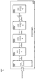
Fig. 2 is the block diagram of the accumulator system in system in package (SIP) shell, and described accumulator system has a plurality of memory devices in the unidirectional daisy chain cascade of being configured in;
Fig. 3 is the block diagram of the accumulator system in system in package (SIP) shell, and described accumulator system has a plurality of memory devices in the bidirectional daisy chain cascade of being configured in;
Fig. 4 A is the block diagram of flash memory controller;
Fig. 4 B is the block diagram with the flash memory controller of CPU;
Fig. 5 is the block diagram of SIP, and described SIP comprises main flash memory and a plurality of memory devices of unidirectional daisy chain cascade configuration;
Fig. 6 is the block diagram of SIP, and described SIP comprises main flash memory and a plurality of memory devices of bidirectional daisy chain cascade configuration;
The block diagram that Fig. 7 is the accumulator system that realizes in SIP layout;
Fig. 8 is the block diagram of the accumulator system in SIP shell, and described accumulator system has a plurality of memory devices that are configured in the unidirectional daisy chain cascade that comprises a plurality of connections;
Fig. 9 is the block diagram of the accumulator system in SIP shell, and described accumulator system has a plurality of memory devices that are configured in the bidirectional daisy chain cascade of sharing public port.
Embodiment
Below exemplary embodiment of the present invention is described.
Fig. 1 illustrates the integrated scintillator device 100 that has flash memory 135 and be embedded in the steering logic in single integrated circuit.Described steering logic comprises host interface 110, storage buffer 115, state machine 125, internal register 120 and the error correction logic 130 for communicating by letter with external system, described state machine 125 and described storer 135 interfaces.For example, in read operation, order and address date that internal register 120 receives from host interface 110.State machine 125 receives these data and according to flash memory 135 described in this read operation access.The alphabetic data that state machine 125 receives from flash memory 135, obtains the data of asking thus.After by error correction logic 130 checkings, the data of asking are sent to storage buffer 115 for sending to external system.There is " the OneNAND that other details in the operation of flash memory of controller of embedding is announced on Dec 23rd, 2005 in Samsung Electronics
tMspecification " describe in 1.2 editions.
The block diagram of Fig. 2 illustrates the accumulator system 200 in system in package (SIP) shell 210, and described accumulator system 200 has a plurality of memory devices 230a-n in the daisy chain cascade arrangement of being configured in.SIP is single package or the module that comprises a plurality of integrated circuit (chip).SIP can be designed as an autonomous system or system element and moves, and carries out the many or repertoire such as the electronic system of mobile phone, personal computer or digital music player.Chip encapsulation or inside modules can be orthogonal stacking or horizontal positioned side by side each other.Chip is typically connected by the wire of enclosing in encapsulation.Selectively, chip can connect with solder bump, for bonding them together with " flip-chip " technology.
SIP can comprise several circuit components and the passive element being arranged on same substrate.For example, SIP can be included in the processor of realizing in special IC (ASIC), storer and resistor and the capacitor relevant to described circuit of realizing in discrete circuit tube core.Such combination of element makes in single package, to set up complete function unit, avoids increasing necessity that a plurality of outer members produce function system.Use the design of SIP equipment, due to its complicacy that has reduced the system of SIP outside, be particularly useful in the limited space environment such as laptop computer, MP3 player and mobile phone.
In response to the communicating by letter of external system or other instruction, flash controller 220 can be communicated by letter with one or more flash memory 230a-n arranging with unidirectional daisy chain cascade.In unidirectional daisy chain cascade configuration, each equipment in daisy chain cascading sends to follow-up equipment by received signal with together with produced signal, thereby provides single communication path 235 by these equipment.Therefore signal path 235 comprises a plurality of link 235a-n of equipment room, and represents singlely from flash controller 220 and by the flash memory 230a-n in daisy chain cascading, returns to the one-way communication stream of flash controller 220.In addition, link 235a-n can be two-way, connects driver and the acceptor circuit of each equipment.
In this example, flash controller 220 sends order and data-signal to the first flash memory 230a(" flash memory A " in daisy chain cascading by signal path 235a).Flash memory 230a is according to received command response, and described response can comprise obtains data, the data writing of storage or carries out other operation.Flash memory 230a export subsequently and the order that responds relevant arbitrary data and reception to next memory devices 230b.On the contrary, if the order receiving is not addressed to flash memory 230a, equipment 230a exports the order receiving and does not carry out other operation.Flash memory 230a can be by comparing and determine whether described order is addressed to it with the device identifier that is stored in storer 230a with the relevant address field of described order.
Flash memory 230b receives the arbitrary data from the order of storer 230a and storer 230a generation.As storer 230a formerly, flash memory 230b is in response to being addressed to its any order, and the data of output command and any generation are to next equipment 230c.In signal path 235, for all devices, repeat this continuous communication, until order is received by last flash memory 230n.Flash memory 230n is according to command response, and any data that produce by signal path 235n output command and memory devices 230a-n are to flash controller 220.As a result, the communication of accumulator system 200 is sent to all devices in daisy chain cascading by signal path 235.Signal path 235 can comprise that one or more pin of equipment room or wire connect, and can serial or parallel transmission signal.Referring to U.S. Patent application NO.11/324, 023(" Multiple Independent Serial Link Memory (a plurality of independent serial link memory) "), U.S. Patent application NO.11/495, 278(" Daisy Chain Cascading Devices (daisy chain cascading devices) "), U.S. Patent application NO.11/521, 734(" Asynchronous ID Generation (asynchronous ID generate) ") and U.S. Provisional Application NO.60/802, 645(" serial interconnection of Serial Interconnection of Memory Devices(memory devices) "), obtain about the serial communication of memory devices and the exemplary techniques of daisy chain cascade configuration.More than whole being taught in herein by reference of application is included in herein just as all illustrating.
In this example, accumulator system 200 comprises a plurality of flash memory 230a-n, is configured in this way: from the input signal of flash controller 220, be transferred to the first scintillator device and be transferred to flash controller 220 from the output signal of last equipment 230n.In the exemplary embodiment, all signals (comprising input data and order from flash controller 220) come downwards to last memory devices 230n from first memory equipment 230a.Therefore, all input and output signals one-way transmission on signal path 235.Input command can comprise the address such as the target device of one of them of memory devices 230a-n.At system initialization or during powering on, can certainly as each scintillator device 230a-n, distribute distinctive device address by flash controller 220 or scintillator device 230a-n, or can be through allocating in advance such as the hardware programming of One Time Programmable (OTP) array.When flash controller 220 issues have the order of destination device address, corresponding scintillator device (one of them of equipment 230a-n) is carried out received order.All the other equipment of scintillator device 230a-n are corresponding to the order receiving with " bypass " mode operation, and transmission command is to follow-up equipment in daisy chain cascade arrangement, and there is no other operation.
By identifier (ID) generative process, in each that can be in memory devices 230a-n, set up destination device address.The U.S. Patent application NO.11/521 all including by reference, 734 " the asynchronous ID of Asynchronous ID Generation(generates) ", be included in the exemplary techniques that produces ID in daisy chain cascade arrangement on a plurality of memory devices.In one exemplary embodiment, each the equipment 230a-n in daisy chain cascading has generative circuit (not shown).When controller 220 sends " generating ID " order to equipment 230a-n, the generative circuit of the first equipment 230a receives the first value of self-controller 220, according to this value, generates device id.Device id can be stored in the register of the first equipment 230a, and is used for determining whether order and address are addressed to equipment 230a.This generative circuit also produces the second value of being revised by the first value increment, by the first equipment 230a, is transferred to follow-up equipment 230b.The generative circuit of the second equipment 230b produces device id according to the second value, and transmits value to the three equipment 230c that revise.Repeat this process, until last the equipment 230n apparatus for establishing ID in daisy chain cascading.
Selectively, scintillator device 230a-n can select the addressing of signal (not shown) by connecting the signal path use equipment of each equipment 230a-n and flash memory controller 220.In this embodiment, flash memory controller 220 can select signal to the scintillator device 220a of order addressing by transmitting apparatus, thereby the equipment 220a of making responds and carry out received order.Remaining scintillator device 220b-n can not receiving equipment selects signal, and the order that therefore transmission receives is to the follow-up equipment in daisy chain cascade arrangement, and there is no other operation.
Flash memory is a kind of nonvolatile memory, can keep stored data, and without power supply source or frequent refresh operation.In optional embodiment, can replace with the nonvolatile memory of other type one or more flash memory 230a-n, or can integrate with in scintillator device 230a-n.Equally, such as the volatile memory of static RAM (SRAM) and dynamic RAM (DRAM), can integrate with in flash memory 230a-n.This optional embodiment also requires controller 220 according to the standard operation of storer, or essential additional or alternative Memory Controller.Below with reference to Fig. 4, describe the operation of flash memory controller in detail.
Fig. 3 is the block diagram of the accumulator system 300 in system shown level encapsulation (SIP) shell 310, has a plurality of flash memory 330a-n in the daisy chain cascade arrangement of being configured in.Accumulator system 300 is than the system 200 of Fig. 2, and flash controller 320 can mode as identical with equipment 230a-n in controller 220 configure with flash memory 330a-n to a certain extent, as the description carrying out above with reference to Fig. 2.But the controller 320 of native system 300 is with equipment 330a-n through communicating by letter at bidirectional daisy chain cascade, signal path 334 and the signal in 335, described signal path 334 and 335 is included in a plurality of link 334a-n, the 335a-n of input/output port connection device.Signal path 334 and 335 represents signal of communication stream, and it passes through the flash memory 330a-n of daisy chain cascading from flash controller 320 and by signal path 334, through signal path 335, turns back to flash controller 320.
Flash controller 320 communicates by system interface and the external system (not shown) such as computer system.System interface provides a plurality of signal paths between flash controller 320 and external system, described signal path sending and receiving memory data, order, clock signal and other signal relevant to control store system 300.
In response to the communicating by letter of external system or other instruction, flash controller 320 can be communicated by letter with one or more flash memory 330a-n arranging with bidirectional daisy chain cascade.In the bidirectional daisy chain cascade configuration of describing herein, flash controller 320 sends order and data-signal to the first flash memory 330a(" flash memory A " in daisy chain cascading by signal path 334a).In daisy chain cascading, each flash memory 330a-n sends through signal path 334 signal receiving and arrives follow-up equipment, until last equipment in daisy chain cascading (" flash memory N " 330n) receives described signal.
Each equipment 330a-n response is addressed to its signal receiving, and the signal generating that sends response through signal path 335 is to flash controller 320.For example, flash controller can send be addressed to flash memory B330b " reading " order for obtaining the data that are stored on this equipment.Order through flash memory A330a(through link 334a-b) and received by flash memory B330b.Flash memory B carrys out response command by sending the data of asking through link 335a-b to flash controller 320.Flash memory B also sends a command to flash memory C330c, and it sends again order further by being cascaded to last equipment-flash memory N330n.
Under some conditions, flash controller 320 can be the more than one memory devices of particular command addressing.Further, for above-mentioned example, described order also can be asked the data from flash memory C330c.In this case, equipment can receive the order from flash memory B330b, and by arriving flash controller 320 through link 335c output data to send the data of being asked.As a result, flash controller 320 can receive the two the data of asking from flash memory B330b and C330c through signal path 335.
Therefore, flash memory controller 320 can control and data signal to control flash memory 330a-n by transmission, described controling and data signal by equipment 330a-n with the first direction by bidirectional daisy chain cascade (, signal path 334) transmission, and return to responding communication to controller 320 by the signal with the second direction through bidirectional daisy chain cascade (that is, signal path 335) transmission.Memory devices 330a-n also can be arranged to return and control and data signal flash controller 320, and wherein, last equipment (flash memory 330n) in cascade is sent and control and data signal by signal path 335.
The entrance and exit link that the bidirectional daisy chain cascade of accumulator system 300 is each memory devices 330a-n coupled equipment in providing along signal path 334,335 to daisy chain cascading.In optional embodiment, equipment can communicate by the link in other configuration.For example, in daisy chain cascading, the memory devices except last equipment 330n can be configured to transfer responsive communication to last equipment.Flash memory B330b can receive from the order of last equipment 330a and data transfer responsive communication and turn back to last equipment 330a, for being received by flash controller 320, rather than (or additional) by communications to next equipment 330c.Flash memory B can also be arranged to and when receiving such as the order of high priority or some type communication of data, carry out this operation.This configuration can realize in one or more equipment in daisy chain cascading, and can be for reducing the delay of some operation in accumulator system 300.
Fig. 4 A is the block diagram of exemplary flash memory controller 400.The embodiment of described controller 400 can realize on integrated circuit lead separately, and is used in SIP as the flash memory controller 220,320,820 and 920 referring to the accumulator system separately 200,300,800 in above-mentioned and following Fig. 2,3,8 and 9 and 900.Controller 400 also can be embedded in flash memory chip, controller 400 and storer operate as main flash memory, and described main flash memory can be implemented conduct referring to the accumulator system separately 500 of following Fig. 5 and Fig. 6 and 600 main flash memory 520 and 620.
Flash memory controller 400 comprises system interface 480, steering logic 410 and flash memory interface 490.System interface 480 is applicable to communicate by letter with external host system, and can be configured to or non-flash interface or other memory devices interface used other memory devices such as double data rate (DDR) dynamic RAM (DRAM), RAMBUS DRAM interface, serial ATA (SATA) interface, IEEE1394, MMC interface or USB (universal serial bus) (USB).Selectively, system interface 480 can be positioned apart with steering logic 410, is embodied as a specific installation, or be positioned at the internal system of communicating by letter with flash controller 400.
Flash memory interface 490 is the physical flash interface for one or more flash memory communication of same daisy chain cascade arrangement.U.S. Provisional Application NO.60/839, and 329(" NAND Flash Memory Device(and non-flash memory) ") the middle exemplary blink interface of describing, it proposes as a whole by quoting in full herein.In addition, flash memory interface 490 and steering logic 410 can be configured to control and non-flash memory, provide or non-DRAM or other interface at said system interface 480 simultaneously.Therefore, flash memory controller 400 can be used as " mixing " controller, by or non-or other interface communicate by letter to provide the control to non-flash memory with external host system.
Flash memory controller 400, as realized in an embodiment of the present invention, can be used as system controller, by the order and the data control memory equipment that send through cascade.These orders and data are received at each memory devices (not shown) by device controller, and it is carried out again response and controls the algorithm of the order of memory array separately.
In exemplary " reading " operation, the request of data that flash memory controller 400 receives from external host system (not shown) at system interface 480.The logical address of the data of storing on one or more memory devices that request of data instruction memory controller 400 is controlled.Steering logic 410 is determined corresponding physical address.By flash memory interface 490, controller 400 sends " read command " with the physical address of institute's request msg by the cascade of memory devices.Target memory device is carried out " reading " algorithm for obtaining asked data, and it can comprise that loading the page arrives device page buffer.The data that target memory device is asked in flash memory interface 490 transmission are to flash memory controller 400.Steering logic 410 is verified the data that receive and corrects a mistake in error correcting code (ECC) module 435.Steering logic 410 is loaded subsequently the data of asking and is arrived impact damper RAM420, and it is transferred to external host system through system interface 480.
Programming operation is similar to above-mentioned read operation, and wherein, flash memory controller 400 receives the data that will store one or more memory devices into from external host system.Steering logic 410, based on one or more data-mapping, distribution and loss balancing scheme, is determined the physical address of storage data.Given physical address, flash memory controller 400 is by cascade transmission " program command " and data and definite physical address of memory devices.Target memory device loading data writes data to page buffer and initialization " programming " algorithm the physical address of being determined by Memory Controller 400.After this write operation, target device sends " program verification " signal and is used to indicate and writes whether success.Target memory device repeats " programming " and " program verification " circulation, until " program verification " indicates successful write operation.
In a plurality of cascade memories equipment of control as above, the communication protocol that Memory Controller 400 is used is different from the agreement of controlling a plurality of equipment in single memory equipment or multiple spot layout.For example, when select target memory devices, Memory Controller 400 must send the address corresponding to memory devices.This address (or aforementioned target device ID) can be integrated in the structure of control command, thereby makes the particular device in cascade selected.
The block diagram of Fig. 4 B is described the second exemplary flash memory controller 401, and it can be configured in above-mentioned referring in one or more configuration described in flash controller 400.Flash controller 401 can be with the difference of controller 400, and it comprises CPU (central processing unit) (CPU) 470, can be used in more complicated task.
Except above-mentioned, referring to the described element of Fig. 4 A, flash memory controller 401 comprises crystal oscillator (Xtal) 476, and it provides the reference clock signal being connected with controll block with clock generator.Clock generator and controll block 475 provide various clock signals to CPU470, flash controller 495 and system interface 465.CPU470 communicates by letter with other subsystem by common bus 485.RAM and ROM circuit 496 are also connected to common bus 485, and wherein, RAM provides buffer memory and ROM store executable code.Flash controller 495 comprises physical flash interface, ECC piece and file and memory management block.By physical flash interface access scintillator device.ECC piece checks and corrects the data from institute's access of scintillator device.Conversion, loss balancing algorithm and other function that file and memory management block provide logic to arrive physical address.
Fig. 5 is the block diagram that is encapsulated in another example memory system 500 in SIP shell.System comprises a plurality of equipment that are encapsulated in SIP shell, and described shell holds main flash memory 520 and is configured in a plurality of flash memory 530a-n in unidirectional daisy chain cascade along signal path 535.Signal path 535 comprises a plurality of link 535a-n of connection device.Main flash memory 520 sends order and data to first memory equipment 530n at link 535a, and link 535n reception from daisy chain cascading in the responding communication of last memory devices 530n.
Fig. 6 is the block diagram of the optional flash memory system 600 in SIP shell 610, and system 600 has main flash memory 620, for controlling a plurality of flash memory 620a-n.Described equipment is configured in bidirectional daisy chain cascade along the signal path 634,635 that comprises the link 634a-n, the 635a-n that connect described equipment.System 600 can comprise above-mentioned about the feature described in Fig. 2,3 and 5 system 200,300 and 500.
The block diagram that Fig. 7 is the example memory system 700 that realizes in SIP layout.Described system comprises a plurality of chips, comprises with vertical stacking and is assemblied on wiring board 750 and is contained in Memory Controller 720 and a plurality of memory devices 730a-c in SIP shell 710.SIP shell 710 can comprise for sealing medium or resin at surrounding package system element, thereby provide hard encapsulation that element is fixed therein.Chip 720,730a-c are connected by the wire 735 being encapsulated in equally in shell 710.Selectively, chip 720,730a-c also can be placed by horizontal Tile each other according to design constraint in shell 710, or can connect they are combined with " flip-chip " technology with solder bump.
The block diagram of Fig. 7 provides the illustrative example of the accumulator system 700 realizing in SIP shell 710.The element of system 700 as above can be configured by difference according to the design requirement of specific embodiment with being connected.For example, Fig. 2,3,5,6,8 and 9 accumulator system 200,300,500,600,800 and 900 can be implemented as the similar accumulator system of system 700 with Fig. 7.Thereby this accumulator system provides the SIP shell of a plurality of memory devices that hold in Memory Controller and daisy chain cascade arrangement, described controller is controlled described memory devices by cascade.
System in package (SIP) is to realize the example of embodiment of the single shape factor of accumulator system 200,300,500,600,800 and 900.Accumulator system also can realize in other suitable equipment or public support assembly, and wherein, element Memory Controller is arranged to external system and communicates by letter with memory devices.For example, accumulator system can be implemented as circuit board, and such as storage card, its middle controller and memory devices comprise the chip that is coupled to described plate, and via the signal path communication on circuit board.
Fig. 8 is the block diagram of the accumulator system 800 in SIP shell 810, and described storage system 800 has a plurality of memory devices 830a-n that are configured in the unidirectional daisy chain cascade that comprises a plurality of connections.Flash controller 820 is by through comprising that the order of signal path 834,835 transmission of the link between each memory devices 830a-n carrys out opertaing device 830a-n.Described configuration is similar to the configuration of the system 200 of Fig. 2, but different, and each of equipment 830a-n is connected rather than one by two unidirectional paths.Accumulator system also can comprise above-mentioned system 200, the 300 described features referring to Fig. 2 and 3, comprises the flash controller 820 of a plurality of flash memory 830a-n of addressing.In this embodiment, flash controller 820 sends by link 834a order and data are transmitted by link 834a-d by signal path 834.The signal path 835 that links 835b-n in response to the data of ordering by comprising is transmitted, and is received by flash controller 820.The order that flash controller sends and data also can turn back to flash controller through link 835n.Therefore the signal path 835 that, comprises unidirectional daisy chain cascade be divided into be exclusively used in transmission from the order of flash controller 820 and the first 834a-d(top, path of data) and be exclusively used in the second 830b-n(bottom, path of response data of each generation of transmission memory equipment 830a-n).
In optional embodiment, accumulator system 800 goes for realizing above-mentioned main flash memory.In this case, flash controller 920 can be used main flash memory to substitute, and controls as described in Figure 5 flash memory 930a-n.
Fig. 9 is the block diagram of the accumulator system 900 in SIP shell 910, and described system 900 has a plurality of memory devices 930a-n that the bidirectional daisy chain cascade of being configured in is shared general input/output port.Flash controller 820 is by through comprising that the order of signal path 935 transmission of the link between each memory devices 930a-n carrys out opertaing device 930a-n.Described configuration is similar to the configuration of the system 300 of Fig. 3, but different, and each of link 935b-n is single bi-directional chaining rather than two one-way linkages.Described link 935b-n can be connected to the general input/output port of each equipment 930a-n, thereby makes it possible to carry out two-way communication by each link 935b-n.Order and data that flash controller 920 sends are transferred to each memory devices 930a-n by signal path 935a-n.Data in response to order are also transmitted by signal path 935b-n, and are transferred to the flash controller at link 935a place.Therefore bidirectional daisy chain cascade can be used on the signal path 935 that comprises a plurality of link 935a-n that share general input/output port.
In optional embodiment, accumulator system 900 goes for realizing above-mentioned main flash memory.In this case, flash controller 920 can be used main flash memory to substitute, and controls as described in Figure 6 flash memory 930a-n.
Although the present invention is with reference to the special demonstration of its example embodiment and description, those of ordinary skill in the art is to be understood that the various variations that can carry out in form and details in the situation that not departing from the claimed scope of the invention of claims.
Claims (18)
1. a Nonvolatile memory devices, comprising:
Nonvolatile memory array, it comprises a plurality of, and each piece comprises a plurality of pages, and described nonvolatile memory array is configured to read data, the data in programmed page and the data in erase block in the page;
The first port, it is configured to receive order from controller, and described order comprises address information;
The second port, it is coupled to the input port of another Nonvolatile memory devices;
The 3rd port, it is configured to receive the first output from described another Nonvolatile memory devices;
The 4th port, it is configured to provide the second output to described controller; And
Device determiner, it is configured to determine whether the address information of described order identifies described Nonvolatile memory devices,
Definite in response to not mating, the order receiving is output to described another Nonvolatile memory devices by described the second port, and
In response to coupling, determine,
In the situation that described order is read for data, process described order with nonvolatile memory array described in access, and in response to reading order, read the addressed page of described nonvolatile memory array,
In described order, for programme in the situation that, process described order with nonvolatile memory array described in access, and in response to the programme addressed page of described nonvolatile memory array of program command, and
In the situation that described order is used for wiping, processes described order with nonvolatile memory array described in access, and in response to program command, wipe the addressed piece of described nonvolatile memory array.
2. Nonvolatile memory devices according to claim 1, wherein, the data that read are sent to described another Nonvolatile memory devices by described the second output port.
3. Nonvolatile memory devices according to claim 1, wherein, the data that read are sent to described controller by described the 4th port as the second output.
4. Nonvolatile memory devices according to claim 1, wherein:
Described the 3rd port is also configured to receive the programming data as described the first output from described another Nonvolatile memory devices; And
Described the 4th port is also configured to provide received programming data to described controller.
5. Nonvolatile memory devices according to claim 1, wherein:
Described the first port is also configured to receive order and programming data from described controller; And
Described the 4th port is also configured to described controller, provide read data from described nonvolatile memory array.
6. Nonvolatile memory devices according to claim 1, wherein, described the first port, the second port, the 3rd port and the 4th port are serial or parallel ports.
7. Nonvolatile memory devices according to claim 1, wherein, described device determiner is configured to determining device address when system initialization.
8. Nonvolatile memory devices according to claim 1, wherein, described device determiner is configured to actuating unit address when powering on and determines.
9. Nonvolatile memory devices according to claim 1, wherein, when described device determiner is configured to receive from described controller the order that comprises value on described the first port, actuating unit address is determined.
10. Nonvolatile memory devices according to claim 9, wherein, described device determiner is also configured to the value generation device sign based on received.
11. Nonvolatile memory devices according to claim 1, also comprise the register that is configured to memory storage address.
12. Nonvolatile memory devices according to claim 1, wherein, described device determiner is configured to come determining device address based on hardware programming.
13. Nonvolatile memory devices according to claim 12, wherein, described device determiner is configured to come determining device address based on One Time Programmable array.
14. 1 kinds of chips with Nonvolatile memory devices, described Nonvolatile memory devices comprises arbitrary described Nonvolatile memory devices in claim 1 to 15.
15. 1 kinds of encapsulation that comprise arbitrary described Nonvolatile memory devices in controller and one or more claim 1 to 13, described controller comprises the first port, for the first port to one or more Nonvolatile memory devices, provide order and programming data, described controller also comprises the second port, for the 4th port from one or more Nonvolatile memory devices, receives the data that read.
16. encapsulation according to claim 15, wherein, install described one or more Nonvolatile memory devices and described controller in the circuit board each other abreast.
17. encapsulation according to claim 15, wherein, described one or more Nonvolatile memory devices and described controller are installed in vertical stacking ground in the circuit board.
18. encapsulation according to claim 17, wherein, described one or more Nonvolatile memory devices are connected with at least one use solder bump or wire in described controller.
Applications Claiming Priority (8)
| Application Number | Priority Date | Filing Date | Title |
|---|---|---|---|
| US78771006P | 2006-03-28 | 2006-03-28 | |
| US60/787,710 | 2006-03-28 | ||
| US11/496,278 US20070076502A1 (en) | 2005-09-30 | 2006-07-31 | Daisy chain cascading devices |
| US11/496,278 | 2006-07-31 | ||
| US83953406P | 2006-08-23 | 2006-08-23 | |
| US60/839,534 | 2006-08-23 | ||
| US11/639,375 US20070165457A1 (en) | 2005-09-30 | 2006-12-14 | Nonvolatile memory system |
| US11/639,375 | 2006-12-14 |
Related Parent Applications (1)
| Application Number | Title | Priority Date | Filing Date |
|---|---|---|---|
| CN2007800106485A Division CN101410814B (en) | 2006-03-28 | 2007-03-26 | Daisy chain arrangement of non-volatile memories |
Publications (1)
| Publication Number | Publication Date |
|---|---|
| CN103714841A true CN103714841A (en) | 2014-04-09 |
Family
ID=38540751
Family Applications (2)
| Application Number | Title | Priority Date | Filing Date |
|---|---|---|---|
| CN201310261739.3A Pending CN103714841A (en) | 2006-03-28 | 2007-03-26 | A daisy chain arrangement of non-volatile memories |
| CN2007800106485A Expired - Fee Related CN101410814B (en) | 2006-03-28 | 2007-03-26 | Daisy chain arrangement of non-volatile memories |
Family Applications After (1)
| Application Number | Title | Priority Date | Filing Date |
|---|---|---|---|
| CN2007800106485A Expired - Fee Related CN101410814B (en) | 2006-03-28 | 2007-03-26 | Daisy chain arrangement of non-volatile memories |
Country Status (8)
| Country | Link |
|---|---|
| US (2) | US20070165457A1 (en) |
| EP (3) | EP1999601A4 (en) |
| JP (2) | JP5189072B2 (en) |
| KR (2) | KR101314893B1 (en) |
| CN (2) | CN103714841A (en) |
| CA (1) | CA2644593A1 (en) |
| TW (1) | TW201433921A (en) |
| WO (1) | WO2007109888A1 (en) |
Families Citing this family (88)
| Publication number | Priority date | Publication date | Assignee | Title |
|---|---|---|---|---|
| US7296129B2 (en) | 2004-07-30 | 2007-11-13 | International Business Machines Corporation | System, method and storage medium for providing a serialized memory interface with a bus repeater |
| US7539800B2 (en) * | 2004-07-30 | 2009-05-26 | International Business Machines Corporation | System, method and storage medium for providing segment level sparing |
| US7512762B2 (en) | 2004-10-29 | 2009-03-31 | International Business Machines Corporation | System, method and storage medium for a memory subsystem with positional read data latency |
| US7299313B2 (en) | 2004-10-29 | 2007-11-20 | International Business Machines Corporation | System, method and storage medium for a memory subsystem command interface |
| US7331010B2 (en) | 2004-10-29 | 2008-02-12 | International Business Machines Corporation | System, method and storage medium for providing fault detection and correction in a memory subsystem |
| EP1932158A4 (en) | 2005-09-30 | 2008-10-15 | Mosaid Technologies Inc | Memory with output control |
| US11948629B2 (en) | 2005-09-30 | 2024-04-02 | Mosaid Technologies Incorporated | Non-volatile memory device with concurrent bank operations |
| US7652922B2 (en) | 2005-09-30 | 2010-01-26 | Mosaid Technologies Incorporated | Multiple independent serial link memory |
| US7478259B2 (en) | 2005-10-31 | 2009-01-13 | International Business Machines Corporation | System, method and storage medium for deriving clocks in a memory system |
| US7685392B2 (en) | 2005-11-28 | 2010-03-23 | International Business Machines Corporation | Providing indeterminate read data latency in a memory system |
| US7669086B2 (en) | 2006-08-02 | 2010-02-23 | International Business Machines Corporation | Systems and methods for providing collision detection in a memory system |
| US8700818B2 (en) * | 2006-09-29 | 2014-04-15 | Mosaid Technologies Incorporated | Packet based ID generation for serially interconnected devices |
| US7870459B2 (en) | 2006-10-23 | 2011-01-11 | International Business Machines Corporation | High density high reliability memory module with power gating and a fault tolerant address and command bus |
| US20080113525A1 (en) * | 2006-11-15 | 2008-05-15 | Sandisk Il Ltd. | Compact solid state drive and processor assembly |
| US8331361B2 (en) * | 2006-12-06 | 2012-12-11 | Mosaid Technologies Incorporated | Apparatus and method for producing device identifiers for serially interconnected devices of mixed type |
| US7853727B2 (en) | 2006-12-06 | 2010-12-14 | Mosaid Technologies Incorporated | Apparatus and method for producing identifiers regardless of mixed device type in a serial interconnection |
| US7650459B2 (en) * | 2006-12-21 | 2010-01-19 | Intel Corporation | High speed interface for non-volatile memory |
| US7721140B2 (en) | 2007-01-02 | 2010-05-18 | International Business Machines Corporation | Systems and methods for improving serviceability of a memory system |
| US8010710B2 (en) * | 2007-02-13 | 2011-08-30 | Mosaid Technologies Incorporated | Apparatus and method for identifying device type of serially interconnected devices |
| US7728619B1 (en) * | 2007-03-30 | 2010-06-01 | Cypress Semiconductor Corporation | Circuit and method for cascading programmable impedance matching in a multi-chip system |
| US20080301355A1 (en) * | 2007-05-30 | 2008-12-04 | Phison Electronics Corp. | Flash memory information reading/writing method and storage device using the same |
| US20080306723A1 (en) * | 2007-06-08 | 2008-12-11 | Luca De Ambroggi | Emulated Combination Memory Device |
| US7688652B2 (en) * | 2007-07-18 | 2010-03-30 | Mosaid Technologies Incorporated | Storage of data in memory via packet strobing |
| US20090063786A1 (en) | 2007-08-29 | 2009-03-05 | Hakjune Oh | Daisy-chain memory configuration and usage |
| US8825939B2 (en) * | 2007-12-12 | 2014-09-02 | Conversant Intellectual Property Management Inc. | Semiconductor memory device suitable for interconnection in a ring topology |
| US8781053B2 (en) * | 2007-12-14 | 2014-07-15 | Conversant Intellectual Property Management Incorporated | Clock reproducing and timing method in a system having a plurality of devices |
| US8467486B2 (en) * | 2007-12-14 | 2013-06-18 | Mosaid Technologies Incorporated | Memory controller with flexible data alignment to clock |
| WO2009079014A1 (en) * | 2007-12-18 | 2009-06-25 | President And Fellows Of Harvard College | Nand implementation for high bandwidth applications |
| US9495116B2 (en) * | 2007-12-26 | 2016-11-15 | Sandisk Il Ltd. | Storage device coordinator and a host device that includes the same |
| US20090182977A1 (en) * | 2008-01-16 | 2009-07-16 | S. Aqua Semiconductor Llc | Cascaded memory arrangement |
| US20110235260A1 (en) * | 2008-04-09 | 2011-09-29 | Apacer Technology Inc. | Dram module with solid state disk |
| US7983051B2 (en) * | 2008-04-09 | 2011-07-19 | Apacer Technology Inc. | DRAM module with solid state disk |
| US8843691B2 (en) * | 2008-06-25 | 2014-09-23 | Stec, Inc. | Prioritized erasure of data blocks in a flash storage device |
| US8161313B2 (en) * | 2008-09-30 | 2012-04-17 | Mosaid Technologies Incorporated | Serial-connected memory system with duty cycle correction |
| US8181056B2 (en) | 2008-09-30 | 2012-05-15 | Mosaid Technologies Incorporated | Serial-connected memory system with output delay adjustment |
| WO2010041093A1 (en) * | 2008-10-09 | 2010-04-15 | Federico Tiziani | Virtualized ecc nand |
| US8472199B2 (en) | 2008-11-13 | 2013-06-25 | Mosaid Technologies Incorporated | System including a plurality of encapsulated semiconductor chips |
| KR101687038B1 (en) * | 2008-12-18 | 2016-12-15 | 노바칩스 캐나다 인크. | Error detection method and a system including one or more memory devices |
| US8880970B2 (en) * | 2008-12-23 | 2014-11-04 | Conversant Intellectual Property Management Inc. | Error detection method and a system including one or more memory devices |
| US8055936B2 (en) * | 2008-12-31 | 2011-11-08 | Pitney Bowes Inc. | System and method for data recovery in a disabled integrated circuit |
| US8060453B2 (en) * | 2008-12-31 | 2011-11-15 | Pitney Bowes Inc. | System and method for funds recovery from an integrated postal security device |
| US7894230B2 (en) | 2009-02-24 | 2011-02-22 | Mosaid Technologies Incorporated | Stacked semiconductor devices including a master device |
| US8832353B2 (en) * | 2009-04-07 | 2014-09-09 | Sandisk Technologies Inc. | Host stop-transmission handling |
| US8132045B2 (en) * | 2009-06-16 | 2012-03-06 | SanDisk Technologies, Inc. | Program failure handling in nonvolatile memory |
| US8307241B2 (en) * | 2009-06-16 | 2012-11-06 | Sandisk Technologies Inc. | Data recovery in multi-level cell nonvolatile memory |
| US9779057B2 (en) | 2009-09-11 | 2017-10-03 | Micron Technology, Inc. | Autonomous memory architecture |
| TWI423033B (en) * | 2009-12-22 | 2014-01-11 | Ind Tech Res Inst | A cascade device of serial bus with clock and cascade method |
| US8966208B2 (en) * | 2010-02-25 | 2015-02-24 | Conversant Ip Management Inc. | Semiconductor memory device with plural memory die and controller die |
| US8582382B2 (en) * | 2010-03-23 | 2013-11-12 | Mosaid Technologies Incorporated | Memory system having a plurality of serially connected devices |
| US8463959B2 (en) * | 2010-05-31 | 2013-06-11 | Mosaid Technologies Incorporated | High-speed interface for daisy-chained devices |
| US8582373B2 (en) | 2010-08-31 | 2013-11-12 | Micron Technology, Inc. | Buffer die in stacks of memory dies and methods |
| KR101796116B1 (en) | 2010-10-20 | 2017-11-10 | 삼성전자 주식회사 | Semiconductor device, memory module and memory system having the same and operating method thereof |
| US8793419B1 (en) * | 2010-11-22 | 2014-07-29 | Sk Hynix Memory Solutions Inc. | Interface between multiple controllers |
| CN102183548B (en) * | 2011-03-16 | 2013-02-27 | 复旦大学 | Failed bump positioning method based on daisy chain loop design |
| US9390049B2 (en) * | 2011-06-03 | 2016-07-12 | Micron Technology, Inc. | Logical unit address assignment |
| CN102436426A (en) * | 2011-11-04 | 2012-05-02 | 忆正存储技术(武汉)有限公司 | Embedded memorizer and embedded memorizer system |
| US8825967B2 (en) * | 2011-12-08 | 2014-09-02 | Conversant Intellectual Property Management Inc. | Independent write and read control in serially-connected devices |
| US8797799B2 (en) * | 2012-01-05 | 2014-08-05 | Conversant Intellectual Property Management Inc. | Device selection schemes in multi chip package NAND flash memory system |
| US8954825B2 (en) * | 2012-03-06 | 2015-02-10 | Micron Technology, Inc. | Apparatuses and methods including error correction code organization |
| KR20130107841A (en) * | 2012-03-23 | 2013-10-02 | 삼성전자주식회사 | Memory system |
| US9569402B2 (en) | 2012-04-20 | 2017-02-14 | International Business Machines Corporation | 3-D stacked multiprocessor structure with vertically aligned identical layout operating processors in independent mode or in sharing mode running faster components |
| US9391047B2 (en) | 2012-04-20 | 2016-07-12 | International Business Machines Corporation | 3-D stacked and aligned processors forming a logical processor with power modes controlled by respective set of configuration parameters |
| CN102662383B (en) * | 2012-05-29 | 2014-11-19 | 张二浩 | Realizing method for controlling chain of chain control system |
| CN202677849U (en) * | 2012-06-04 | 2013-01-16 | 旭丽电子(广州)有限公司 | Portable storage apparatus |
| US8804452B2 (en) * | 2012-07-31 | 2014-08-12 | Micron Technology, Inc. | Data interleaving module |
| JP6166517B2 (en) * | 2012-09-04 | 2017-07-19 | ラピスセミコンダクタ株式会社 | Electronic device and address setting method |
| US9471484B2 (en) | 2012-09-19 | 2016-10-18 | Novachips Canada Inc. | Flash memory controller having dual mode pin-out |
| US10079044B2 (en) * | 2012-12-20 | 2018-09-18 | Advanced Micro Devices, Inc. | Processor with host and slave operating modes stacked with memory |
| US9037902B2 (en) | 2013-03-15 | 2015-05-19 | Sandisk Technologies Inc. | Flash memory techniques for recovering from write interrupt resulting from voltage fault |
| US9779138B2 (en) | 2013-08-13 | 2017-10-03 | Micron Technology, Inc. | Methods and systems for autonomous memory searching |
| US10003675B2 (en) | 2013-12-02 | 2018-06-19 | Micron Technology, Inc. | Packet processor receiving packets containing instructions, data, and starting location and generating packets containing instructions and data |
| US9600183B2 (en) * | 2014-09-22 | 2017-03-21 | Intel Corporation | Apparatus, system and method for determining comparison information based on memory data |
| US10216678B2 (en) * | 2014-10-07 | 2019-02-26 | Infineon Technologies Ag | Serial peripheral interface daisy chain communication with an in-frame response |
| KR102291806B1 (en) * | 2015-04-20 | 2021-08-24 | 삼성전자주식회사 | Nonvolatile memory system and operation method thereof |
| JP2017045415A (en) * | 2015-08-28 | 2017-03-02 | 株式会社東芝 | Memory system |
| TWI612788B (en) * | 2015-12-21 | 2018-01-21 | 視動自動化科技股份有限公司 | Communication system with train bus architecture |
| US20170187894A1 (en) * | 2015-12-28 | 2017-06-29 | Kabushiki Kaisha Toshiba | System and method for print job forwarding |
| US10057209B2 (en) * | 2016-07-28 | 2018-08-21 | Qualcomm Incorporated | Time-sequenced multi-device address assignment |
| KR20180034778A (en) | 2016-09-27 | 2018-04-05 | 삼성전자주식회사 | Electronic device configured to provide bypass path to non-directly connected storage device among serially connected storage devices, storage device included therein, computing system including the same, and method of communicating therewith |
| US10381327B2 (en) * | 2016-10-06 | 2019-08-13 | Sandisk Technologies Llc | Non-volatile memory system with wide I/O memory die |
| US10572344B2 (en) * | 2017-04-27 | 2020-02-25 | Texas Instruments Incorporated | Accessing error statistics from DRAM memories having integrated error correction |
| JP6978670B2 (en) | 2017-12-07 | 2021-12-08 | 富士通株式会社 | Arithmetic processing unit and control method of arithmetic processing unit |
| CN109101451A (en) * | 2018-07-12 | 2018-12-28 | 比飞力(深圳)科技有限公司 | Chip-in series circuit calculates equipment and communication means |
| EP3694173B1 (en) | 2019-02-08 | 2022-09-21 | Palantir Technologies Inc. | Isolating applications associated with multiple tenants within a computing platform |
| CN112286842B (en) * | 2019-07-22 | 2023-07-04 | 苏州库瀚信息科技有限公司 | Bus for memory controller and memory device interconnection |
| US11163490B2 (en) * | 2019-09-17 | 2021-11-02 | Micron Technology, Inc. | Programmable engine for data movement |
| US11416422B2 (en) * | 2019-09-17 | 2022-08-16 | Micron Technology, Inc. | Memory chip having an integrated data mover |
| US11397694B2 (en) | 2019-09-17 | 2022-07-26 | Micron Technology, Inc. | Memory chip connecting a system on a chip and an accelerator chip |
Family Cites Families (111)
| Publication number | Priority date | Publication date | Assignee | Title |
|---|---|---|---|---|
| US6085A (en) * | 1849-02-06 | Hoisting apparatus | ||
| EP0179605B1 (en) * | 1984-10-17 | 1992-08-19 | Fujitsu Limited | Semiconductor memory device having a serial data input circuit and a serial data output circuit |
| US4683555A (en) * | 1985-01-22 | 1987-07-28 | Texas Instruments Incorporated | Serial accessed semiconductor memory with reconfigureable shift registers |
| US4730308A (en) * | 1985-10-04 | 1988-03-08 | International Business Machines Corporation | Interface between a computer bus and a serial packet link |
| JPS62152050A (en) * | 1985-12-26 | 1987-07-07 | Nec Corp | Semiconductor memory |
| JPS63113624A (en) * | 1986-10-30 | 1988-05-18 | Tokyo Electric Co Ltd | Printer interface for electronic scale |
| DE69030858T2 (en) * | 1989-03-15 | 1998-01-29 | Oki Electric Ind Co Ltd | SERIAL INPUT PARALLEL OUTPUT CONVERSION SWITCHING |
| US5126808A (en) * | 1989-10-23 | 1992-06-30 | Advanced Micro Devices, Inc. | Flash EEPROM array with paged erase architecture |
| US5243703A (en) * | 1990-04-18 | 1993-09-07 | Rambus, Inc. | Apparatus for synchronously generating clock signals in a data processing system |
| US5204669A (en) * | 1990-08-30 | 1993-04-20 | Datacard Corporation | Automatic station identification where function modules automatically initialize |
| US5319598A (en) * | 1990-12-10 | 1994-06-07 | Hughes Aircraft Company | Nonvolatile serially programmable devices |
| US5132635A (en) * | 1991-03-05 | 1992-07-21 | Ast Research, Inc. | Serial testing of removable circuit boards on a backplane bus |
| US5249270A (en) * | 1991-03-29 | 1993-09-28 | Echelon Corporation | Development system protocol |
| US5430859A (en) * | 1991-07-26 | 1995-07-04 | Sundisk Corporation | Solid state memory system including plural memory chips and a serialized bus |
| US6230233B1 (en) * | 1991-09-13 | 2001-05-08 | Sandisk Corporation | Wear leveling techniques for flash EEPROM systems |
| US5361227A (en) * | 1991-12-19 | 1994-11-01 | Kabushiki Kaisha Toshiba | Non-volatile semiconductor memory device and memory system using the same |
| KR950000761B1 (en) * | 1992-01-15 | 1995-01-28 | 삼성전자 주식회사 | Apparatus for synchronizing serial input signals |
| US5313096A (en) * | 1992-03-16 | 1994-05-17 | Dense-Pac Microsystems, Inc. | IC chip package having chip attached to and wire bonded within an overlying substrate |
| JP3088180B2 (en) * | 1992-03-26 | 2000-09-18 | 日本電気アイシーマイコンシステム株式会社 | Serial input interface circuit |
| JPH0793219A (en) * | 1993-09-20 | 1995-04-07 | Olympus Optical Co Ltd | Information processor |
| US5602780A (en) * | 1993-10-20 | 1997-02-11 | Texas Instruments Incorporated | Serial to parallel and parallel to serial architecture for a RAM based FIFO memory |
| US5452259A (en) * | 1993-11-15 | 1995-09-19 | Micron Technology Inc. | Multiport memory with pipelined serial input |
| US5404460A (en) * | 1994-01-28 | 1995-04-04 | Vlsi Technology, Inc. | Method for configuring multiple identical serial I/O devices to unique addresses through a serial bus |
| US5596724A (en) * | 1994-02-04 | 1997-01-21 | Advanced Micro Devices | Input/output data port with a parallel and serial interface |
| DE4429433C1 (en) * | 1994-08-19 | 1995-10-26 | Siemens Ag | Address association method for modular stored program controller |
| KR0142367B1 (en) * | 1995-02-04 | 1998-07-15 | 김광호 | Erase verifying circuit for nonvolatile semiconductor memory having dolumn redundancy |
| US5636342A (en) * | 1995-02-17 | 1997-06-03 | Dell Usa, L.P. | Systems and method for assigning unique addresses to agents on a system management bus |
| US5812796A (en) * | 1995-08-18 | 1998-09-22 | General Magic, Inc. | Support structures for an intelligent low power serial bus |
| JP3693721B2 (en) * | 1995-11-10 | 2005-09-07 | Necエレクトロニクス株式会社 | Microcomputer with built-in flash memory and test method thereof |
| KR100211760B1 (en) * | 1995-12-28 | 1999-08-02 | 윤종용 | Data i/o path control circuit of semiconductor memory device having multi-bank structure |
| KR0170723B1 (en) * | 1995-12-29 | 1999-03-30 | 김광호 | Semiconductor memory device having duale bank |
| US7166495B2 (en) * | 1996-02-20 | 2007-01-23 | Micron Technology, Inc. | Method of fabricating a multi-die semiconductor package assembly |
| JPH09231740A (en) * | 1996-02-21 | 1997-09-05 | Nec Corp | Semiconductor memory |
| US5938750A (en) * | 1996-06-28 | 1999-08-17 | Intel Corporation | Method and apparatus for a memory card bus design |
| US5941974A (en) * | 1996-11-29 | 1999-08-24 | Motorola, Inc. | Serial interface with register selection which uses clock counting, chip select pulsing, and no address bits |
| KR100243335B1 (en) * | 1996-12-31 | 2000-02-01 | 김영환 | Daisy chain type memory device having refresh circuit |
| KR100272037B1 (en) * | 1997-02-27 | 2000-12-01 | 니시무로 타이죠 | Non volatile simiconductor memory |
| GB2329792A (en) * | 1997-08-20 | 1999-03-31 | Nokia Telecommunications Oy | Identification signals enable a transceiver module to correctly configure itself to an attached functional module |
| US6253292B1 (en) * | 1997-08-22 | 2001-06-26 | Seong Tae Jhang | Distributed shared memory multiprocessor system based on a unidirectional ring bus using a snooping scheme |
| JPH1166841A (en) * | 1997-08-22 | 1999-03-09 | Mitsubishi Electric Corp | Semiconductor storage device |
| JP4039532B2 (en) * | 1997-10-02 | 2008-01-30 | 株式会社ルネサステクノロジ | Semiconductor integrated circuit device |
| US6378018B1 (en) * | 1997-10-10 | 2002-04-23 | Intel Corporation | Memory device and system including a low power interface |
| US5937425A (en) * | 1997-10-16 | 1999-08-10 | M-Systems Flash Disk Pioneers Ltd. | Flash file system optimized for page-mode flash technologies |
| US6102963A (en) * | 1997-12-29 | 2000-08-15 | Vantis Corporation | Electrically erasable and reprogrammable, nonvolatile integrated storage device with in-system programming and verification (ISPAV) capabilities for supporting in-system reconfiguring of PLD's |
| GB2339044B (en) * | 1998-03-02 | 2003-06-04 | Lexar Media Inc | Flash memory card with enhanced operating mode detection and user-friendly interfacing system |
| US6085290A (en) * | 1998-03-10 | 2000-07-04 | Nexabit Networks, Llc | Method of and apparatus for validating data read out of a multi port internally cached dynamic random access memory (AMPIC DRAM) |
| WO2001006371A1 (en) * | 1998-07-21 | 2001-01-25 | Seagate Technology Llc | Improved memory system apparatus and method |
| JP4601737B2 (en) * | 1998-10-28 | 2010-12-22 | 株式会社東芝 | Memory embedded logic LSI |
| JP2000149564A (en) * | 1998-10-30 | 2000-05-30 | Mitsubishi Electric Corp | Semiconductor memory device |
| KR100284742B1 (en) * | 1998-12-28 | 2001-04-02 | 윤종용 | Memory device with the minimum number of I / O sense amplifiers |
| JP3853537B2 (en) * | 1999-04-30 | 2006-12-06 | 株式会社日立製作所 | Semiconductor memory file system |
| US7130958B2 (en) * | 2003-12-02 | 2006-10-31 | Super Talent Electronics, Inc. | Serial interface to flash-memory chip using PCI-express-like packets and packed data for partial-page writes |
| US6567023B1 (en) * | 1999-09-17 | 2003-05-20 | Kabushiki Kaisha Toshiba | Analog to digital to analog converter for multi-valued current data using internal binary voltage |
| US6680904B1 (en) * | 1999-12-27 | 2004-01-20 | Orckit Communications Ltd. | Bi-directional chaining of network access ports |
| US20050160218A1 (en) * | 2004-01-20 | 2005-07-21 | Sun-Teck See | Highly integrated mass storage device with an intelligent flash controller |
| US6442098B1 (en) * | 2000-02-08 | 2002-08-27 | Alliance Semiconductor | High performance multi-bank compact synchronous DRAM architecture |
| US7181635B2 (en) * | 2000-03-13 | 2007-02-20 | Analog Devices, Inc. | Method for placing a device in a selected mode of operation |
| US6535948B1 (en) * | 2000-05-31 | 2003-03-18 | Agere Systems Inc. | Serial interface unit |
| US6754807B1 (en) * | 2000-08-31 | 2004-06-22 | Stmicroelectronics, Inc. | System and method for managing vertical dependencies in a digital signal processor |
| US6317352B1 (en) | 2000-09-18 | 2001-11-13 | Intel Corporation | Apparatus for implementing a buffered daisy chain connection between a memory controller and memory modules |
| US6853557B1 (en) * | 2000-09-20 | 2005-02-08 | Rambus, Inc. | Multi-channel memory architecture |
| US6658509B1 (en) * | 2000-10-03 | 2003-12-02 | Intel Corporation | Multi-tier point-to-point ring memory interface |
| US6718432B1 (en) * | 2001-03-22 | 2004-04-06 | Netlogic Microsystems, Inc. | Method and apparatus for transparent cascading of multiple content addressable memory devices |
| US6732221B2 (en) * | 2001-06-01 | 2004-05-04 | M-Systems Flash Disk Pioneers Ltd | Wear leveling of static areas in flash memory |
| US6996644B2 (en) * | 2001-06-06 | 2006-02-07 | Conexant Systems, Inc. | Apparatus and methods for initializing integrated circuit addresses |
| KR100413762B1 (en) * | 2001-07-02 | 2003-12-31 | 삼성전자주식회사 | Semiconductor memory device having adjustable banks and method thereof |
| CN101515263B (en) * | 2001-07-25 | 2011-05-25 | 索尼公司 | Interface device |
| US6928501B2 (en) * | 2001-10-15 | 2005-08-09 | Silicon Laboratories, Inc. | Serial device daisy chaining method and apparatus |
| US6763426B1 (en) * | 2001-12-27 | 2004-07-13 | Cypress Semiconductor Corporation | Cascadable content addressable memory (CAM) device and architecture |
| JP3916953B2 (en) * | 2001-12-28 | 2007-05-23 | 日本テキサス・インスツルメンツ株式会社 | Variable time division multiplexing transmission system |
| JP4204226B2 (en) * | 2001-12-28 | 2009-01-07 | 日本テキサス・インスツルメンツ株式会社 | Device identification method, data transmission method, device identifier assigning apparatus, and device |
| US6799235B2 (en) * | 2002-01-02 | 2004-09-28 | Intel Corporation | Daisy chain latency reduction |
| US6958940B2 (en) * | 2002-02-28 | 2005-10-25 | Renesas Technology Corp. | Nonvolatile semiconductor memory device capable of realizing optimized erasing operation in a memory array |
| US7234052B2 (en) * | 2002-03-08 | 2007-06-19 | Samsung Electronics Co., Ltd | System boot using NAND flash memory and method thereof |
| KR100456596B1 (en) * | 2002-05-08 | 2004-11-09 | 삼성전자주식회사 | Method of erasing floating trap type non-volatile memory device |
| US7073022B2 (en) * | 2002-05-23 | 2006-07-04 | International Business Machines Corporation | Serial interface for a data storage array |
| US7062601B2 (en) * | 2002-06-28 | 2006-06-13 | Mosaid Technologies Incorporated | Method and apparatus for interconnecting content addressable memory devices |
| KR100499686B1 (en) * | 2002-07-23 | 2005-07-07 | 주식회사 디지털웨이 | Portable flash memory extended memory capacity |
| CA2396632A1 (en) * | 2002-07-31 | 2004-01-31 | Mosaid Technologies Incorporated | Cam diamond cascade architecture |
| KR100487539B1 (en) * | 2002-09-02 | 2005-05-03 | 삼성전자주식회사 | Nonvolatile semiconductor memory device for connecting to serial advanced techonology attachement cable |
| US7032039B2 (en) * | 2002-10-30 | 2006-04-18 | Atmel Corporation | Method for identification of SPI compatible serial memory devices |
| US7308524B2 (en) * | 2003-01-13 | 2007-12-11 | Silicon Pipe, Inc | Memory chain |
| US7085958B2 (en) * | 2003-01-17 | 2006-08-01 | International Business Machines Corporation | System and method for isolating a faulty switch, storage device or SFP in a daisy-chained configuration |
| US7069370B2 (en) * | 2003-01-31 | 2006-06-27 | Toshiba Corporation | USB memory storage apparatus with integrated circuit in a connector |
| US7016213B2 (en) * | 2003-05-13 | 2006-03-21 | Advanced Micro Devices, Inc. | Method for initializing a system including a host and plurality of memory modules connected via a serial memory interconnect |
| JP4547923B2 (en) * | 2003-08-14 | 2010-09-22 | コニカミノルタホールディングス株式会社 | Inkjet recording device |
| US7149823B2 (en) * | 2003-08-29 | 2006-12-12 | Emulex Corporation | System and method for direct memory access from host without processor intervention wherein automatic access to memory during host start up does not occur |
| US20050086413A1 (en) * | 2003-10-15 | 2005-04-21 | Super Talent Electronics Inc. | Capacity Expansion of Flash Memory Device with a Daisy-Chainable Structure and an Integrated Hub |
| US7779212B2 (en) * | 2003-10-17 | 2010-08-17 | Micron Technology, Inc. | Method and apparatus for sending data from multiple sources over a communications bus |
| US7243205B2 (en) * | 2003-11-13 | 2007-07-10 | Intel Corporation | Buffered memory module with implicit to explicit memory command expansion |
| JP5197961B2 (en) * | 2003-12-17 | 2013-05-15 | スタッツ・チップパック・インコーポレイテッド | Multi-chip package module and manufacturing method thereof |
| US7152138B2 (en) * | 2004-01-30 | 2006-12-19 | Hewlett-Packard Development Company, L.P. | System on a chip having a non-volatile imperfect memory |
| KR100559736B1 (en) | 2004-09-22 | 2006-03-10 | 삼성전자주식회사 | Memory system and test method thereof, and hub and memory module of the same |
| KR100597473B1 (en) * | 2004-06-11 | 2006-07-05 | 삼성전자주식회사 | Method of Testing Memory Module and Hub of Memory Module of the same |
| US7254663B2 (en) * | 2004-07-22 | 2007-08-07 | International Business Machines Corporation | Multi-node architecture with daisy chain communication link configurable to operate in unidirectional and bidirectional modes |
| US8375146B2 (en) * | 2004-08-09 | 2013-02-12 | SanDisk Technologies, Inc. | Ring bus structure and its use in flash memory systems |
| US7669027B2 (en) * | 2004-08-19 | 2010-02-23 | Micron Technology, Inc. | Memory command delay balancing in a daisy-chained memory topology |
| KR100705221B1 (en) * | 2004-09-03 | 2007-04-06 | 에스티마이크로일렉트로닉스 엔.브이. | Flash memory device and method of erasing the flash memory cell using the same |
| JP4406339B2 (en) * | 2004-09-21 | 2010-01-27 | 株式会社東芝 | Controller, memory card and control method thereof |
| US20060087013A1 (en) * | 2004-10-21 | 2006-04-27 | Etron Technology, Inc. | Stacked multiple integrated circuit die package assembly |
| US7334070B2 (en) * | 2004-10-29 | 2008-02-19 | International Business Machines Corporation | Multi-channel memory architecture for daisy chained arrangements of nodes with bridging between memory channels |
| EP1851771A2 (en) * | 2005-02-11 | 2007-11-07 | M-Systems Flash Disk Pioneers Ltd. | Nand flash memory system architecture |
| US20070005831A1 (en) * | 2005-06-30 | 2007-01-04 | Peter Gregorius | Semiconductor memory system |
| US20070076502A1 (en) | 2005-09-30 | 2007-04-05 | Pyeon Hong B | Daisy chain cascading devices |
| US7652922B2 (en) | 2005-09-30 | 2010-01-26 | Mosaid Technologies Incorporated | Multiple independent serial link memory |
| US7496777B2 (en) * | 2005-10-12 | 2009-02-24 | Sun Microsystems, Inc. | Power throttling in a memory system |
| US7523282B1 (en) * | 2005-10-27 | 2009-04-21 | Sun Microsystems, Inc. | Clock enable throttling for power savings in a memory subsystem |
| US8364861B2 (en) | 2006-03-28 | 2013-01-29 | Mosaid Technologies Incorporated | Asynchronous ID generation |
| US7546410B2 (en) * | 2006-07-26 | 2009-06-09 | International Business Machines Corporation | Self timed memory chip having an apportionable data bus |
| US7721130B2 (en) * | 2006-11-27 | 2010-05-18 | Qimonda Ag | Apparatus and method for switching an apparatus to a power saving mode |
| US7650459B2 (en) * | 2006-12-21 | 2010-01-19 | Intel Corporation | High speed interface for non-volatile memory |
-
2006
- 2006-12-14 US US11/639,375 patent/US20070165457A1/en not_active Abandoned
-
2007
- 2007-03-15 TW TW103119019A patent/TW201433921A/en unknown
- 2007-03-26 KR KR1020087020432A patent/KR101314893B1/en not_active IP Right Cessation
- 2007-03-26 EP EP07719422A patent/EP1999601A4/en not_active Ceased
- 2007-03-26 CN CN201310261739.3A patent/CN103714841A/en active Pending
- 2007-03-26 JP JP2009501797A patent/JP5189072B2/en not_active Expired - Fee Related
- 2007-03-26 KR KR1020137012902A patent/KR101365827B1/en active IP Right Grant
- 2007-03-26 EP EP11003539A patent/EP2348510A1/en not_active Ceased
- 2007-03-26 CA CA002644593A patent/CA2644593A1/en not_active Abandoned
- 2007-03-26 CN CN2007800106485A patent/CN101410814B/en not_active Expired - Fee Related
- 2007-03-26 WO PCT/CA2007/000488 patent/WO2007109888A1/en active Application Filing
-
2008
- 2008-09-29 EP EP08015337A patent/EP2031516A3/en not_active Ceased
-
2009
- 2009-10-13 US US12/578,115 patent/US20100030951A1/en not_active Abandoned
-
2012
- 2012-09-25 JP JP2012210614A patent/JP5575856B2/en not_active Expired - Fee Related
Also Published As
| Publication number | Publication date |
|---|---|
| JP2013037712A (en) | 2013-02-21 |
| KR101365827B1 (en) | 2014-02-20 |
| KR101314893B1 (en) | 2013-10-04 |
| WO2007109888A1 (en) | 2007-10-04 |
| EP2031516A2 (en) | 2009-03-04 |
| JP5189072B2 (en) | 2013-04-24 |
| CN101410814A (en) | 2009-04-15 |
| US20070165457A1 (en) | 2007-07-19 |
| US20100030951A1 (en) | 2010-02-04 |
| CA2644593A1 (en) | 2007-10-04 |
| EP2031516A3 (en) | 2009-07-15 |
| KR20130073991A (en) | 2013-07-03 |
| CN101410814B (en) | 2013-07-17 |
| EP1999601A4 (en) | 2009-04-08 |
| EP2348510A1 (en) | 2011-07-27 |
| JP5575856B2 (en) | 2014-08-20 |
| JP2009531746A (en) | 2009-09-03 |
| TW201433921A (en) | 2014-09-01 |
| KR20090007280A (en) | 2009-01-16 |
| EP1999601A1 (en) | 2008-12-10 |
Similar Documents
| Publication | Publication Date | Title |
|---|---|---|
| CN101410814B (en) | Daisy chain arrangement of non-volatile memories | |
| US9159380B2 (en) | Bridge device architecture for connecting discrete memory devices to a system | |
| US8134852B2 (en) | Bridge device architecture for connecting discrete memory devices to a system | |
| US10061642B2 (en) | Memory device and system including on chip ECC circuit | |
| TW201030746A (en) | A bridging device having a configurable virtual page size | |
| US20180068981A1 (en) | Semiconductor apparatus and semiconductor system including the same | |
| US10340255B2 (en) | Semiconductor apparatus and semiconductor system including the same | |
| TWI448901B (en) | Nonvolatile memory system | |
| CN101388238A (en) | Flash storage chip an flash array storage system |
Legal Events
| Date | Code | Title | Description |
|---|---|---|---|
| C06 | Publication | ||
| PB01 | Publication | ||
| C10 | Entry into substantive examination | ||
| SE01 | Entry into force of request for substantive examination | ||
| C53 | Correction of patent of invention or patent application | ||
| CB02 | Change of applicant information |
Address after: Ontario, Canada Applicant after: Examine Vincent Zhi Cai management company Address before: Ontario, Canada Applicant before: Mosaid Technologies Inc. |
|
| COR | Change of bibliographic data |
Free format text: CORRECT: APPLICANT; FROM: MOSAID TECHNOLOGIES INC. TO: CONVERSANT INTELLECTUAL PROPERTY MANAGEMENT INC. |
|
| C02 | Deemed withdrawal of patent application after publication (patent law 2001) | ||
| WD01 | Invention patent application deemed withdrawn after publication |
Application publication date: 20140409 |