CN103201835A - Microelectronic package with dual or multiple - etched flip -chip connectors and corresponding manufacturing method - Google Patents
Microelectronic package with dual or multiple - etched flip -chip connectors and corresponding manufacturing method Download PDFInfo
- Publication number
- CN103201835A CN103201835A CN2011800428536A CN201180042853A CN103201835A CN 103201835 A CN103201835 A CN 103201835A CN 2011800428536 A CN2011800428536 A CN 2011800428536A CN 201180042853 A CN201180042853 A CN 201180042853A CN 103201835 A CN103201835 A CN 103201835A
- Authority
- CN
- China
- Prior art keywords
- protruded stigma
- solid metal
- microelectronic element
- scolder
- substrate
- Prior art date
- Legal status (The legal status is an assumption and is not a legal conclusion. Google has not performed a legal analysis and makes no representation as to the accuracy of the status listed.)
- Pending
Links
Images


Classifications
-
- H—ELECTRICITY
- H01—ELECTRIC ELEMENTS
- H01L—SEMICONDUCTOR DEVICES NOT COVERED BY CLASS H10
- H01L23/00—Details of semiconductor or other solid state devices
- H01L23/48—Arrangements for conducting electric current to or from the solid state body in operation, e.g. leads, terminal arrangements ; Selection of materials therefor
-
- H—ELECTRICITY
- H01—ELECTRIC ELEMENTS
- H01L—SEMICONDUCTOR DEVICES NOT COVERED BY CLASS H10
- H01L21/00—Processes or apparatus adapted for the manufacture or treatment of semiconductor or solid state devices or of parts thereof
- H01L21/02—Manufacture or treatment of semiconductor devices or of parts thereof
- H01L21/04—Manufacture or treatment of semiconductor devices or of parts thereof the devices having at least one potential-jump barrier or surface barrier, e.g. PN junction, depletion layer or carrier concentration layer
- H01L21/48—Manufacture or treatment of parts, e.g. containers, prior to assembly of the devices, using processes not provided for in a single one of the subgroups H01L21/06 - H01L21/326
- H01L21/4814—Conductive parts
- H01L21/4846—Leads on or in insulating or insulated substrates, e.g. metallisation
- H01L21/4853—Connection or disconnection of other leads to or from a metallisation, e.g. pins, wires, bumps
-
- H—ELECTRICITY
- H01—ELECTRIC ELEMENTS
- H01L—SEMICONDUCTOR DEVICES NOT COVERED BY CLASS H10
- H01L23/00—Details of semiconductor or other solid state devices
- H01L23/48—Arrangements for conducting electric current to or from the solid state body in operation, e.g. leads, terminal arrangements ; Selection of materials therefor
- H01L23/481—Internal lead connections, e.g. via connections, feedthrough structures
-
- H—ELECTRICITY
- H01—ELECTRIC ELEMENTS
- H01L—SEMICONDUCTOR DEVICES NOT COVERED BY CLASS H10
- H01L23/00—Details of semiconductor or other solid state devices
- H01L23/48—Arrangements for conducting electric current to or from the solid state body in operation, e.g. leads, terminal arrangements ; Selection of materials therefor
- H01L23/488—Arrangements for conducting electric current to or from the solid state body in operation, e.g. leads, terminal arrangements ; Selection of materials therefor consisting of soldered or bonded constructions
- H01L23/498—Leads, i.e. metallisations or lead-frames on insulating substrates, e.g. chip carriers
- H01L23/49811—Additional leads joined to the metallisation on the insulating substrate, e.g. pins, bumps, wires, flat leads
-
- H—ELECTRICITY
- H01—ELECTRIC ELEMENTS
- H01L—SEMICONDUCTOR DEVICES NOT COVERED BY CLASS H10
- H01L24/00—Arrangements for connecting or disconnecting semiconductor or solid-state bodies; Methods or apparatus related thereto
- H01L24/01—Means for bonding being attached to, or being formed on, the surface to be connected, e.g. chip-to-package, die-attach, "first-level" interconnects; Manufacturing methods related thereto
- H01L24/10—Bump connectors ; Manufacturing methods related thereto
- H01L24/11—Manufacturing methods
-
- H—ELECTRICITY
- H01—ELECTRIC ELEMENTS
- H01L—SEMICONDUCTOR DEVICES NOT COVERED BY CLASS H10
- H01L24/00—Arrangements for connecting or disconnecting semiconductor or solid-state bodies; Methods or apparatus related thereto
- H01L24/01—Means for bonding being attached to, or being formed on, the surface to be connected, e.g. chip-to-package, die-attach, "first-level" interconnects; Manufacturing methods related thereto
- H01L24/10—Bump connectors ; Manufacturing methods related thereto
- H01L24/12—Structure, shape, material or disposition of the bump connectors prior to the connecting process
- H01L24/13—Structure, shape, material or disposition of the bump connectors prior to the connecting process of an individual bump connector
-
- H—ELECTRICITY
- H01—ELECTRIC ELEMENTS
- H01L—SEMICONDUCTOR DEVICES NOT COVERED BY CLASS H10
- H01L24/00—Arrangements for connecting or disconnecting semiconductor or solid-state bodies; Methods or apparatus related thereto
- H01L24/01—Means for bonding being attached to, or being formed on, the surface to be connected, e.g. chip-to-package, die-attach, "first-level" interconnects; Manufacturing methods related thereto
- H01L24/10—Bump connectors ; Manufacturing methods related thereto
- H01L24/15—Structure, shape, material or disposition of the bump connectors after the connecting process
- H01L24/16—Structure, shape, material or disposition of the bump connectors after the connecting process of an individual bump connector
-
- H—ELECTRICITY
- H01—ELECTRIC ELEMENTS
- H01L—SEMICONDUCTOR DEVICES NOT COVERED BY CLASS H10
- H01L24/00—Arrangements for connecting or disconnecting semiconductor or solid-state bodies; Methods or apparatus related thereto
- H01L24/80—Methods for connecting semiconductor or other solid state bodies using means for bonding being attached to, or being formed on, the surface to be connected
- H01L24/81—Methods for connecting semiconductor or other solid state bodies using means for bonding being attached to, or being formed on, the surface to be connected using a bump connector
-
- H—ELECTRICITY
- H01—ELECTRIC ELEMENTS
- H01L—SEMICONDUCTOR DEVICES NOT COVERED BY CLASS H10
- H01L21/00—Processes or apparatus adapted for the manufacture or treatment of semiconductor or solid state devices or of parts thereof
- H01L21/02—Manufacture or treatment of semiconductor devices or of parts thereof
- H01L21/04—Manufacture or treatment of semiconductor devices or of parts thereof the devices having at least one potential-jump barrier or surface barrier, e.g. PN junction, depletion layer or carrier concentration layer
- H01L21/50—Assembly of semiconductor devices using processes or apparatus not provided for in a single one of the subgroups H01L21/06 - H01L21/326, e.g. sealing of a cap to a base of a container
- H01L21/56—Encapsulations, e.g. encapsulation layers, coatings
- H01L21/563—Encapsulation of active face of flip-chip device, e.g. underfilling or underencapsulation of flip-chip, encapsulation preform on chip or mounting substrate
-
- H—ELECTRICITY
- H01—ELECTRIC ELEMENTS
- H01L—SEMICONDUCTOR DEVICES NOT COVERED BY CLASS H10
- H01L2224/00—Indexing scheme for arrangements for connecting or disconnecting semiconductor or solid-state bodies and methods related thereto as covered by H01L24/00
- H01L2224/01—Means for bonding being attached to, or being formed on, the surface to be connected, e.g. chip-to-package, die-attach, "first-level" interconnects; Manufacturing methods related thereto
- H01L2224/02—Bonding areas; Manufacturing methods related thereto
- H01L2224/04—Structure, shape, material or disposition of the bonding areas prior to the connecting process
- H01L2224/0401—Bonding areas specifically adapted for bump connectors, e.g. under bump metallisation [UBM]
-
- H—ELECTRICITY
- H01—ELECTRIC ELEMENTS
- H01L—SEMICONDUCTOR DEVICES NOT COVERED BY CLASS H10
- H01L2224/00—Indexing scheme for arrangements for connecting or disconnecting semiconductor or solid-state bodies and methods related thereto as covered by H01L24/00
- H01L2224/01—Means for bonding being attached to, or being formed on, the surface to be connected, e.g. chip-to-package, die-attach, "first-level" interconnects; Manufacturing methods related thereto
- H01L2224/02—Bonding areas; Manufacturing methods related thereto
- H01L2224/04—Structure, shape, material or disposition of the bonding areas prior to the connecting process
- H01L2224/05—Structure, shape, material or disposition of the bonding areas prior to the connecting process of an individual bonding area
- H01L2224/0554—External layer
- H01L2224/05575—Plural external layers
- H01L2224/0558—Plural external layers being stacked
-
- H—ELECTRICITY
- H01—ELECTRIC ELEMENTS
- H01L—SEMICONDUCTOR DEVICES NOT COVERED BY CLASS H10
- H01L2224/00—Indexing scheme for arrangements for connecting or disconnecting semiconductor or solid-state bodies and methods related thereto as covered by H01L24/00
- H01L2224/01—Means for bonding being attached to, or being formed on, the surface to be connected, e.g. chip-to-package, die-attach, "first-level" interconnects; Manufacturing methods related thereto
- H01L2224/02—Bonding areas; Manufacturing methods related thereto
- H01L2224/04—Structure, shape, material or disposition of the bonding areas prior to the connecting process
- H01L2224/05—Structure, shape, material or disposition of the bonding areas prior to the connecting process of an individual bonding area
- H01L2224/0554—External layer
- H01L2224/05599—Material
- H01L2224/056—Material with a principal constituent of the material being a metal or a metalloid, e.g. boron [B], silicon [Si], germanium [Ge], arsenic [As], antimony [Sb], tellurium [Te] and polonium [Po], and alloys thereof
- H01L2224/05638—Material with a principal constituent of the material being a metal or a metalloid, e.g. boron [B], silicon [Si], germanium [Ge], arsenic [As], antimony [Sb], tellurium [Te] and polonium [Po], and alloys thereof the principal constituent melting at a temperature of greater than or equal to 950°C and less than 1550°C
- H01L2224/05644—Gold [Au] as principal constituent
-
- H—ELECTRICITY
- H01—ELECTRIC ELEMENTS
- H01L—SEMICONDUCTOR DEVICES NOT COVERED BY CLASS H10
- H01L2224/00—Indexing scheme for arrangements for connecting or disconnecting semiconductor or solid-state bodies and methods related thereto as covered by H01L24/00
- H01L2224/01—Means for bonding being attached to, or being formed on, the surface to be connected, e.g. chip-to-package, die-attach, "first-level" interconnects; Manufacturing methods related thereto
- H01L2224/02—Bonding areas; Manufacturing methods related thereto
- H01L2224/04—Structure, shape, material or disposition of the bonding areas prior to the connecting process
- H01L2224/06—Structure, shape, material or disposition of the bonding areas prior to the connecting process of a plurality of bonding areas
- H01L2224/061—Disposition
- H01L2224/0612—Layout
-
- H—ELECTRICITY
- H01—ELECTRIC ELEMENTS
- H01L—SEMICONDUCTOR DEVICES NOT COVERED BY CLASS H10
- H01L2224/00—Indexing scheme for arrangements for connecting or disconnecting semiconductor or solid-state bodies and methods related thereto as covered by H01L24/00
- H01L2224/01—Means for bonding being attached to, or being formed on, the surface to be connected, e.g. chip-to-package, die-attach, "first-level" interconnects; Manufacturing methods related thereto
- H01L2224/10—Bump connectors; Manufacturing methods related thereto
- H01L2224/11—Manufacturing methods
- H01L2224/114—Manufacturing methods by blanket deposition of the material of the bump connector
-
- H—ELECTRICITY
- H01—ELECTRIC ELEMENTS
- H01L—SEMICONDUCTOR DEVICES NOT COVERED BY CLASS H10
- H01L2224/00—Indexing scheme for arrangements for connecting or disconnecting semiconductor or solid-state bodies and methods related thereto as covered by H01L24/00
- H01L2224/01—Means for bonding being attached to, or being formed on, the surface to be connected, e.g. chip-to-package, die-attach, "first-level" interconnects; Manufacturing methods related thereto
- H01L2224/10—Bump connectors; Manufacturing methods related thereto
- H01L2224/11—Manufacturing methods
- H01L2224/1147—Manufacturing methods using a lift-off mask
- H01L2224/11472—Profile of the lift-off mask
-
- H—ELECTRICITY
- H01—ELECTRIC ELEMENTS
- H01L—SEMICONDUCTOR DEVICES NOT COVERED BY CLASS H10
- H01L2224/00—Indexing scheme for arrangements for connecting or disconnecting semiconductor or solid-state bodies and methods related thereto as covered by H01L24/00
- H01L2224/01—Means for bonding being attached to, or being formed on, the surface to be connected, e.g. chip-to-package, die-attach, "first-level" interconnects; Manufacturing methods related thereto
- H01L2224/10—Bump connectors; Manufacturing methods related thereto
- H01L2224/11—Manufacturing methods
- H01L2224/116—Manufacturing methods by patterning a pre-deposited material
-
- H—ELECTRICITY
- H01—ELECTRIC ELEMENTS
- H01L—SEMICONDUCTOR DEVICES NOT COVERED BY CLASS H10
- H01L2224/00—Indexing scheme for arrangements for connecting or disconnecting semiconductor or solid-state bodies and methods related thereto as covered by H01L24/00
- H01L2224/01—Means for bonding being attached to, or being formed on, the surface to be connected, e.g. chip-to-package, die-attach, "first-level" interconnects; Manufacturing methods related thereto
- H01L2224/10—Bump connectors; Manufacturing methods related thereto
- H01L2224/11—Manufacturing methods
- H01L2224/119—Methods of manufacturing bump connectors involving a specific sequence of method steps
- H01L2224/11901—Methods of manufacturing bump connectors involving a specific sequence of method steps with repetition of the same manufacturing step
-
- H—ELECTRICITY
- H01—ELECTRIC ELEMENTS
- H01L—SEMICONDUCTOR DEVICES NOT COVERED BY CLASS H10
- H01L2224/00—Indexing scheme for arrangements for connecting or disconnecting semiconductor or solid-state bodies and methods related thereto as covered by H01L24/00
- H01L2224/01—Means for bonding being attached to, or being formed on, the surface to be connected, e.g. chip-to-package, die-attach, "first-level" interconnects; Manufacturing methods related thereto
- H01L2224/10—Bump connectors; Manufacturing methods related thereto
- H01L2224/12—Structure, shape, material or disposition of the bump connectors prior to the connecting process
- H01L2224/13—Structure, shape, material or disposition of the bump connectors prior to the connecting process of an individual bump connector
- H01L2224/13001—Core members of the bump connector
- H01L2224/1301—Shape
- H01L2224/13016—Shape in side view
- H01L2224/13017—Shape in side view being non uniform along the bump connector
-
- H—ELECTRICITY
- H01—ELECTRIC ELEMENTS
- H01L—SEMICONDUCTOR DEVICES NOT COVERED BY CLASS H10
- H01L2224/00—Indexing scheme for arrangements for connecting or disconnecting semiconductor or solid-state bodies and methods related thereto as covered by H01L24/00
- H01L2224/01—Means for bonding being attached to, or being formed on, the surface to be connected, e.g. chip-to-package, die-attach, "first-level" interconnects; Manufacturing methods related thereto
- H01L2224/10—Bump connectors; Manufacturing methods related thereto
- H01L2224/12—Structure, shape, material or disposition of the bump connectors prior to the connecting process
- H01L2224/13—Structure, shape, material or disposition of the bump connectors prior to the connecting process of an individual bump connector
- H01L2224/13001—Core members of the bump connector
- H01L2224/1301—Shape
- H01L2224/13016—Shape in side view
- H01L2224/13018—Shape in side view comprising protrusions or indentations
-
- H—ELECTRICITY
- H01—ELECTRIC ELEMENTS
- H01L—SEMICONDUCTOR DEVICES NOT COVERED BY CLASS H10
- H01L2224/00—Indexing scheme for arrangements for connecting or disconnecting semiconductor or solid-state bodies and methods related thereto as covered by H01L24/00
- H01L2224/01—Means for bonding being attached to, or being formed on, the surface to be connected, e.g. chip-to-package, die-attach, "first-level" interconnects; Manufacturing methods related thereto
- H01L2224/10—Bump connectors; Manufacturing methods related thereto
- H01L2224/12—Structure, shape, material or disposition of the bump connectors prior to the connecting process
- H01L2224/13—Structure, shape, material or disposition of the bump connectors prior to the connecting process of an individual bump connector
- H01L2224/13001—Core members of the bump connector
- H01L2224/1302—Disposition
- H01L2224/13021—Disposition the bump connector being disposed in a recess of the surface
-
- H—ELECTRICITY
- H01—ELECTRIC ELEMENTS
- H01L—SEMICONDUCTOR DEVICES NOT COVERED BY CLASS H10
- H01L2224/00—Indexing scheme for arrangements for connecting or disconnecting semiconductor or solid-state bodies and methods related thereto as covered by H01L24/00
- H01L2224/01—Means for bonding being attached to, or being formed on, the surface to be connected, e.g. chip-to-package, die-attach, "first-level" interconnects; Manufacturing methods related thereto
- H01L2224/10—Bump connectors; Manufacturing methods related thereto
- H01L2224/12—Structure, shape, material or disposition of the bump connectors prior to the connecting process
- H01L2224/13—Structure, shape, material or disposition of the bump connectors prior to the connecting process of an individual bump connector
- H01L2224/13001—Core members of the bump connector
- H01L2224/13075—Plural core members
- H01L2224/1308—Plural core members being stacked
- H01L2224/13082—Two-layer arrangements
-
- H—ELECTRICITY
- H01—ELECTRIC ELEMENTS
- H01L—SEMICONDUCTOR DEVICES NOT COVERED BY CLASS H10
- H01L2224/00—Indexing scheme for arrangements for connecting or disconnecting semiconductor or solid-state bodies and methods related thereto as covered by H01L24/00
- H01L2224/01—Means for bonding being attached to, or being formed on, the surface to be connected, e.g. chip-to-package, die-attach, "first-level" interconnects; Manufacturing methods related thereto
- H01L2224/10—Bump connectors; Manufacturing methods related thereto
- H01L2224/12—Structure, shape, material or disposition of the bump connectors prior to the connecting process
- H01L2224/13—Structure, shape, material or disposition of the bump connectors prior to the connecting process of an individual bump connector
- H01L2224/13001—Core members of the bump connector
- H01L2224/13099—Material
- H01L2224/131—Material with a principal constituent of the material being a metal or a metalloid, e.g. boron [B], silicon [Si], germanium [Ge], arsenic [As], antimony [Sb], tellurium [Te] and polonium [Po], and alloys thereof
- H01L2224/13138—Material with a principal constituent of the material being a metal or a metalloid, e.g. boron [B], silicon [Si], germanium [Ge], arsenic [As], antimony [Sb], tellurium [Te] and polonium [Po], and alloys thereof the principal constituent melting at a temperature of greater than or equal to 950°C and less than 1550°C
- H01L2224/13144—Gold [Au] as principal constituent
-
- H—ELECTRICITY
- H01—ELECTRIC ELEMENTS
- H01L—SEMICONDUCTOR DEVICES NOT COVERED BY CLASS H10
- H01L2224/00—Indexing scheme for arrangements for connecting or disconnecting semiconductor or solid-state bodies and methods related thereto as covered by H01L24/00
- H01L2224/01—Means for bonding being attached to, or being formed on, the surface to be connected, e.g. chip-to-package, die-attach, "first-level" interconnects; Manufacturing methods related thereto
- H01L2224/10—Bump connectors; Manufacturing methods related thereto
- H01L2224/12—Structure, shape, material or disposition of the bump connectors prior to the connecting process
- H01L2224/13—Structure, shape, material or disposition of the bump connectors prior to the connecting process of an individual bump connector
- H01L2224/13001—Core members of the bump connector
- H01L2224/13099—Material
- H01L2224/131—Material with a principal constituent of the material being a metal or a metalloid, e.g. boron [B], silicon [Si], germanium [Ge], arsenic [As], antimony [Sb], tellurium [Te] and polonium [Po], and alloys thereof
- H01L2224/13138—Material with a principal constituent of the material being a metal or a metalloid, e.g. boron [B], silicon [Si], germanium [Ge], arsenic [As], antimony [Sb], tellurium [Te] and polonium [Po], and alloys thereof the principal constituent melting at a temperature of greater than or equal to 950°C and less than 1550°C
- H01L2224/13147—Copper [Cu] as principal constituent
-
- H—ELECTRICITY
- H01—ELECTRIC ELEMENTS
- H01L—SEMICONDUCTOR DEVICES NOT COVERED BY CLASS H10
- H01L2224/00—Indexing scheme for arrangements for connecting or disconnecting semiconductor or solid-state bodies and methods related thereto as covered by H01L24/00
- H01L2224/01—Means for bonding being attached to, or being formed on, the surface to be connected, e.g. chip-to-package, die-attach, "first-level" interconnects; Manufacturing methods related thereto
- H01L2224/10—Bump connectors; Manufacturing methods related thereto
- H01L2224/15—Structure, shape, material or disposition of the bump connectors after the connecting process
- H01L2224/16—Structure, shape, material or disposition of the bump connectors after the connecting process of an individual bump connector
- H01L2224/161—Disposition
- H01L2224/16151—Disposition the bump connector connecting between a semiconductor or solid-state body and an item not being a semiconductor or solid-state body, e.g. chip-to-substrate, chip-to-passive
- H01L2224/16221—Disposition the bump connector connecting between a semiconductor or solid-state body and an item not being a semiconductor or solid-state body, e.g. chip-to-substrate, chip-to-passive the body and the item being stacked
- H01L2224/16225—Disposition the bump connector connecting between a semiconductor or solid-state body and an item not being a semiconductor or solid-state body, e.g. chip-to-substrate, chip-to-passive the body and the item being stacked the item being non-metallic, e.g. insulating substrate with or without metallisation
- H01L2224/16227—Disposition the bump connector connecting between a semiconductor or solid-state body and an item not being a semiconductor or solid-state body, e.g. chip-to-substrate, chip-to-passive the body and the item being stacked the item being non-metallic, e.g. insulating substrate with or without metallisation the bump connector connecting to a bond pad of the item
-
- H—ELECTRICITY
- H01—ELECTRIC ELEMENTS
- H01L—SEMICONDUCTOR DEVICES NOT COVERED BY CLASS H10
- H01L2224/00—Indexing scheme for arrangements for connecting or disconnecting semiconductor or solid-state bodies and methods related thereto as covered by H01L24/00
- H01L2224/01—Means for bonding being attached to, or being formed on, the surface to be connected, e.g. chip-to-package, die-attach, "first-level" interconnects; Manufacturing methods related thereto
- H01L2224/10—Bump connectors; Manufacturing methods related thereto
- H01L2224/15—Structure, shape, material or disposition of the bump connectors after the connecting process
- H01L2224/16—Structure, shape, material or disposition of the bump connectors after the connecting process of an individual bump connector
- H01L2224/161—Disposition
- H01L2224/16151—Disposition the bump connector connecting between a semiconductor or solid-state body and an item not being a semiconductor or solid-state body, e.g. chip-to-substrate, chip-to-passive
- H01L2224/16221—Disposition the bump connector connecting between a semiconductor or solid-state body and an item not being a semiconductor or solid-state body, e.g. chip-to-substrate, chip-to-passive the body and the item being stacked
- H01L2224/16225—Disposition the bump connector connecting between a semiconductor or solid-state body and an item not being a semiconductor or solid-state body, e.g. chip-to-substrate, chip-to-passive the body and the item being stacked the item being non-metallic, e.g. insulating substrate with or without metallisation
- H01L2224/16238—Disposition the bump connector connecting between a semiconductor or solid-state body and an item not being a semiconductor or solid-state body, e.g. chip-to-substrate, chip-to-passive the body and the item being stacked the item being non-metallic, e.g. insulating substrate with or without metallisation the bump connector connecting to a bonding area protruding from the surface of the item
-
- H—ELECTRICITY
- H01—ELECTRIC ELEMENTS
- H01L—SEMICONDUCTOR DEVICES NOT COVERED BY CLASS H10
- H01L2224/00—Indexing scheme for arrangements for connecting or disconnecting semiconductor or solid-state bodies and methods related thereto as covered by H01L24/00
- H01L2224/01—Means for bonding being attached to, or being formed on, the surface to be connected, e.g. chip-to-package, die-attach, "first-level" interconnects; Manufacturing methods related thereto
- H01L2224/10—Bump connectors; Manufacturing methods related thereto
- H01L2224/15—Structure, shape, material or disposition of the bump connectors after the connecting process
- H01L2224/17—Structure, shape, material or disposition of the bump connectors after the connecting process of a plurality of bump connectors
- H01L2224/1751—Function
- H01L2224/17515—Bump connectors having different functions
-
- H—ELECTRICITY
- H01—ELECTRIC ELEMENTS
- H01L—SEMICONDUCTOR DEVICES NOT COVERED BY CLASS H10
- H01L2224/00—Indexing scheme for arrangements for connecting or disconnecting semiconductor or solid-state bodies and methods related thereto as covered by H01L24/00
- H01L2224/80—Methods for connecting semiconductor or other solid state bodies using means for bonding being attached to, or being formed on, the surface to be connected
- H01L2224/81—Methods for connecting semiconductor or other solid state bodies using means for bonding being attached to, or being formed on, the surface to be connected using a bump connector
- H01L2224/8112—Aligning
- H01L2224/81136—Aligning involving guiding structures, e.g. spacers or supporting members
-
- H—ELECTRICITY
- H01—ELECTRIC ELEMENTS
- H01L—SEMICONDUCTOR DEVICES NOT COVERED BY CLASS H10
- H01L2224/00—Indexing scheme for arrangements for connecting or disconnecting semiconductor or solid-state bodies and methods related thereto as covered by H01L24/00
- H01L2224/80—Methods for connecting semiconductor or other solid state bodies using means for bonding being attached to, or being formed on, the surface to be connected
- H01L2224/81—Methods for connecting semiconductor or other solid state bodies using means for bonding being attached to, or being formed on, the surface to be connected using a bump connector
- H01L2224/8119—Arrangement of the bump connectors prior to mounting
- H01L2224/81193—Arrangement of the bump connectors prior to mounting wherein the bump connectors are disposed on both the semiconductor or solid-state body and another item or body to be connected to the semiconductor or solid-state body
-
- H—ELECTRICITY
- H01—ELECTRIC ELEMENTS
- H01L—SEMICONDUCTOR DEVICES NOT COVERED BY CLASS H10
- H01L2224/00—Indexing scheme for arrangements for connecting or disconnecting semiconductor or solid-state bodies and methods related thereto as covered by H01L24/00
- H01L2224/80—Methods for connecting semiconductor or other solid state bodies using means for bonding being attached to, or being formed on, the surface to be connected
- H01L2224/81—Methods for connecting semiconductor or other solid state bodies using means for bonding being attached to, or being formed on, the surface to be connected using a bump connector
- H01L2224/812—Applying energy for connecting
- H01L2224/81201—Compression bonding
- H01L2224/81203—Thermocompression bonding, e.g. diffusion bonding, pressure joining, thermocompression welding or solid-state welding
-
- H—ELECTRICITY
- H01—ELECTRIC ELEMENTS
- H01L—SEMICONDUCTOR DEVICES NOT COVERED BY CLASS H10
- H01L2224/00—Indexing scheme for arrangements for connecting or disconnecting semiconductor or solid-state bodies and methods related thereto as covered by H01L24/00
- H01L2224/80—Methods for connecting semiconductor or other solid state bodies using means for bonding being attached to, or being formed on, the surface to be connected
- H01L2224/81—Methods for connecting semiconductor or other solid state bodies using means for bonding being attached to, or being formed on, the surface to be connected using a bump connector
- H01L2224/8138—Bonding interfaces outside the semiconductor or solid-state body
- H01L2224/81399—Material
- H01L2224/814—Material with a principal constituent of the material being a metal or a metalloid, e.g. boron [B], silicon [Si], germanium [Ge], arsenic [As], antimony [Sb], tellurium [Te] and polonium [Po], and alloys thereof
-
- H—ELECTRICITY
- H01—ELECTRIC ELEMENTS
- H01L—SEMICONDUCTOR DEVICES NOT COVERED BY CLASS H10
- H01L2224/00—Indexing scheme for arrangements for connecting or disconnecting semiconductor or solid-state bodies and methods related thereto as covered by H01L24/00
- H01L2224/80—Methods for connecting semiconductor or other solid state bodies using means for bonding being attached to, or being formed on, the surface to be connected
- H01L2224/81—Methods for connecting semiconductor or other solid state bodies using means for bonding being attached to, or being formed on, the surface to be connected using a bump connector
- H01L2224/818—Bonding techniques
- H01L2224/81801—Soldering or alloying
- H01L2224/81805—Soldering or alloying involving forming a eutectic alloy at the bonding interface
-
- H—ELECTRICITY
- H01—ELECTRIC ELEMENTS
- H01L—SEMICONDUCTOR DEVICES NOT COVERED BY CLASS H10
- H01L2224/00—Indexing scheme for arrangements for connecting or disconnecting semiconductor or solid-state bodies and methods related thereto as covered by H01L24/00
- H01L2224/80—Methods for connecting semiconductor or other solid state bodies using means for bonding being attached to, or being formed on, the surface to be connected
- H01L2224/81—Methods for connecting semiconductor or other solid state bodies using means for bonding being attached to, or being formed on, the surface to be connected using a bump connector
- H01L2224/818—Bonding techniques
- H01L2224/81801—Soldering or alloying
- H01L2224/81815—Reflow soldering
-
- H—ELECTRICITY
- H01—ELECTRIC ELEMENTS
- H01L—SEMICONDUCTOR DEVICES NOT COVERED BY CLASS H10
- H01L2224/00—Indexing scheme for arrangements for connecting or disconnecting semiconductor or solid-state bodies and methods related thereto as covered by H01L24/00
- H01L2224/80—Methods for connecting semiconductor or other solid state bodies using means for bonding being attached to, or being formed on, the surface to be connected
- H01L2224/81—Methods for connecting semiconductor or other solid state bodies using means for bonding being attached to, or being formed on, the surface to be connected using a bump connector
- H01L2224/818—Bonding techniques
- H01L2224/81801—Soldering or alloying
- H01L2224/8182—Diffusion bonding
-
- H—ELECTRICITY
- H01—ELECTRIC ELEMENTS
- H01L—SEMICONDUCTOR DEVICES NOT COVERED BY CLASS H10
- H01L2224/00—Indexing scheme for arrangements for connecting or disconnecting semiconductor or solid-state bodies and methods related thereto as covered by H01L24/00
- H01L2224/80—Methods for connecting semiconductor or other solid state bodies using means for bonding being attached to, or being formed on, the surface to be connected
- H01L2224/81—Methods for connecting semiconductor or other solid state bodies using means for bonding being attached to, or being formed on, the surface to be connected using a bump connector
- H01L2224/818—Bonding techniques
- H01L2224/81893—Anodic bonding, i.e. bonding by applying a voltage across the interface in order to induce ions migration leading to an irreversible chemical bond
-
- H—ELECTRICITY
- H01—ELECTRIC ELEMENTS
- H01L—SEMICONDUCTOR DEVICES NOT COVERED BY CLASS H10
- H01L2225/00—Details relating to assemblies covered by the group H01L25/00 but not provided for in its subgroups
- H01L2225/03—All the devices being of a type provided for in the same subgroup of groups H01L27/00 - H01L33/648 and H10K99/00
- H01L2225/04—All the devices being of a type provided for in the same subgroup of groups H01L27/00 - H01L33/648 and H10K99/00 the devices not having separate containers
- H01L2225/065—All the devices being of a type provided for in the same subgroup of groups H01L27/00 - H01L33/648 and H10K99/00 the devices not having separate containers the devices being of a type provided for in group H01L27/00
- H01L2225/06503—Stacked arrangements of devices
- H01L2225/06517—Bump or bump-like direct electrical connections from device to substrate
-
- H—ELECTRICITY
- H01—ELECTRIC ELEMENTS
- H01L—SEMICONDUCTOR DEVICES NOT COVERED BY CLASS H10
- H01L2225/00—Details relating to assemblies covered by the group H01L25/00 but not provided for in its subgroups
- H01L2225/03—All the devices being of a type provided for in the same subgroup of groups H01L27/00 - H01L33/648 and H10K99/00
- H01L2225/04—All the devices being of a type provided for in the same subgroup of groups H01L27/00 - H01L33/648 and H10K99/00 the devices not having separate containers
- H01L2225/065—All the devices being of a type provided for in the same subgroup of groups H01L27/00 - H01L33/648 and H10K99/00 the devices not having separate containers the devices being of a type provided for in group H01L27/00
- H01L2225/06503—Stacked arrangements of devices
- H01L2225/0652—Bump or bump-like direct electrical connections from substrate to substrate
-
- H—ELECTRICITY
- H01—ELECTRIC ELEMENTS
- H01L—SEMICONDUCTOR DEVICES NOT COVERED BY CLASS H10
- H01L23/00—Details of semiconductor or other solid state devices
- H01L23/48—Arrangements for conducting electric current to or from the solid state body in operation, e.g. leads, terminal arrangements ; Selection of materials therefor
- H01L23/488—Arrangements for conducting electric current to or from the solid state body in operation, e.g. leads, terminal arrangements ; Selection of materials therefor consisting of soldered or bonded constructions
- H01L23/498—Leads, i.e. metallisations or lead-frames on insulating substrates, e.g. chip carriers
- H01L23/49811—Additional leads joined to the metallisation on the insulating substrate, e.g. pins, bumps, wires, flat leads
- H01L23/49816—Spherical bumps on the substrate for external connection, e.g. ball grid arrays [BGA]
-
- H—ELECTRICITY
- H01—ELECTRIC ELEMENTS
- H01L—SEMICONDUCTOR DEVICES NOT COVERED BY CLASS H10
- H01L23/00—Details of semiconductor or other solid state devices
- H01L23/48—Arrangements for conducting electric current to or from the solid state body in operation, e.g. leads, terminal arrangements ; Selection of materials therefor
- H01L23/488—Arrangements for conducting electric current to or from the solid state body in operation, e.g. leads, terminal arrangements ; Selection of materials therefor consisting of soldered or bonded constructions
- H01L23/498—Leads, i.e. metallisations or lead-frames on insulating substrates, e.g. chip carriers
- H01L23/49822—Multilayer substrates
-
- H—ELECTRICITY
- H01—ELECTRIC ELEMENTS
- H01L—SEMICONDUCTOR DEVICES NOT COVERED BY CLASS H10
- H01L23/00—Details of semiconductor or other solid state devices
- H01L23/48—Arrangements for conducting electric current to or from the solid state body in operation, e.g. leads, terminal arrangements ; Selection of materials therefor
- H01L23/488—Arrangements for conducting electric current to or from the solid state body in operation, e.g. leads, terminal arrangements ; Selection of materials therefor consisting of soldered or bonded constructions
- H01L23/498—Leads, i.e. metallisations or lead-frames on insulating substrates, e.g. chip carriers
- H01L23/49827—Via connections through the substrates, e.g. pins going through the substrate, coaxial cables
-
- H—ELECTRICITY
- H01—ELECTRIC ELEMENTS
- H01L—SEMICONDUCTOR DEVICES NOT COVERED BY CLASS H10
- H01L24/00—Arrangements for connecting or disconnecting semiconductor or solid-state bodies; Methods or apparatus related thereto
- H01L24/01—Means for bonding being attached to, or being formed on, the surface to be connected, e.g. chip-to-package, die-attach, "first-level" interconnects; Manufacturing methods related thereto
- H01L24/02—Bonding areas ; Manufacturing methods related thereto
- H01L24/04—Structure, shape, material or disposition of the bonding areas prior to the connecting process
- H01L24/05—Structure, shape, material or disposition of the bonding areas prior to the connecting process of an individual bonding area
-
- H—ELECTRICITY
- H01—ELECTRIC ELEMENTS
- H01L—SEMICONDUCTOR DEVICES NOT COVERED BY CLASS H10
- H01L25/00—Assemblies consisting of a plurality of individual semiconductor or other solid state devices ; Multistep manufacturing processes thereof
- H01L25/03—Assemblies consisting of a plurality of individual semiconductor or other solid state devices ; Multistep manufacturing processes thereof all the devices being of a type provided for in the same subgroup of groups H01L27/00 - H01L33/00, or in a single subclass of H10K, H10N, e.g. assemblies of rectifier diodes
- H01L25/10—Assemblies consisting of a plurality of individual semiconductor or other solid state devices ; Multistep manufacturing processes thereof all the devices being of a type provided for in the same subgroup of groups H01L27/00 - H01L33/00, or in a single subclass of H10K, H10N, e.g. assemblies of rectifier diodes the devices having separate containers
- H01L25/105—Assemblies consisting of a plurality of individual semiconductor or other solid state devices ; Multistep manufacturing processes thereof all the devices being of a type provided for in the same subgroup of groups H01L27/00 - H01L33/00, or in a single subclass of H10K, H10N, e.g. assemblies of rectifier diodes the devices having separate containers the devices being of a type provided for in group H01L27/00
-
- H—ELECTRICITY
- H01—ELECTRIC ELEMENTS
- H01L—SEMICONDUCTOR DEVICES NOT COVERED BY CLASS H10
- H01L2924/00—Indexing scheme for arrangements or methods for connecting or disconnecting semiconductor or solid-state bodies as covered by H01L24/00
- H01L2924/0001—Technical content checked by a classifier
- H01L2924/00013—Fully indexed content
-
- H—ELECTRICITY
- H01—ELECTRIC ELEMENTS
- H01L—SEMICONDUCTOR DEVICES NOT COVERED BY CLASS H10
- H01L2924/00—Indexing scheme for arrangements or methods for connecting or disconnecting semiconductor or solid-state bodies as covered by H01L24/00
- H01L2924/01—Chemical elements
- H01L2924/01005—Boron [B]
-
- H—ELECTRICITY
- H01—ELECTRIC ELEMENTS
- H01L—SEMICONDUCTOR DEVICES NOT COVERED BY CLASS H10
- H01L2924/00—Indexing scheme for arrangements or methods for connecting or disconnecting semiconductor or solid-state bodies as covered by H01L24/00
- H01L2924/01—Chemical elements
- H01L2924/01006—Carbon [C]
-
- H—ELECTRICITY
- H01—ELECTRIC ELEMENTS
- H01L—SEMICONDUCTOR DEVICES NOT COVERED BY CLASS H10
- H01L2924/00—Indexing scheme for arrangements or methods for connecting or disconnecting semiconductor or solid-state bodies as covered by H01L24/00
- H01L2924/01—Chemical elements
- H01L2924/01013—Aluminum [Al]
-
- H—ELECTRICITY
- H01—ELECTRIC ELEMENTS
- H01L—SEMICONDUCTOR DEVICES NOT COVERED BY CLASS H10
- H01L2924/00—Indexing scheme for arrangements or methods for connecting or disconnecting semiconductor or solid-state bodies as covered by H01L24/00
- H01L2924/01—Chemical elements
- H01L2924/01019—Potassium [K]
-
- H—ELECTRICITY
- H01—ELECTRIC ELEMENTS
- H01L—SEMICONDUCTOR DEVICES NOT COVERED BY CLASS H10
- H01L2924/00—Indexing scheme for arrangements or methods for connecting or disconnecting semiconductor or solid-state bodies as covered by H01L24/00
- H01L2924/01—Chemical elements
- H01L2924/01022—Titanium [Ti]
-
- H—ELECTRICITY
- H01—ELECTRIC ELEMENTS
- H01L—SEMICONDUCTOR DEVICES NOT COVERED BY CLASS H10
- H01L2924/00—Indexing scheme for arrangements or methods for connecting or disconnecting semiconductor or solid-state bodies as covered by H01L24/00
- H01L2924/01—Chemical elements
- H01L2924/01024—Chromium [Cr]
-
- H—ELECTRICITY
- H01—ELECTRIC ELEMENTS
- H01L—SEMICONDUCTOR DEVICES NOT COVERED BY CLASS H10
- H01L2924/00—Indexing scheme for arrangements or methods for connecting or disconnecting semiconductor or solid-state bodies as covered by H01L24/00
- H01L2924/01—Chemical elements
- H01L2924/01029—Copper [Cu]
-
- H—ELECTRICITY
- H01—ELECTRIC ELEMENTS
- H01L—SEMICONDUCTOR DEVICES NOT COVERED BY CLASS H10
- H01L2924/00—Indexing scheme for arrangements or methods for connecting or disconnecting semiconductor or solid-state bodies as covered by H01L24/00
- H01L2924/01—Chemical elements
- H01L2924/01032—Germanium [Ge]
-
- H—ELECTRICITY
- H01—ELECTRIC ELEMENTS
- H01L—SEMICONDUCTOR DEVICES NOT COVERED BY CLASS H10
- H01L2924/00—Indexing scheme for arrangements or methods for connecting or disconnecting semiconductor or solid-state bodies as covered by H01L24/00
- H01L2924/01—Chemical elements
- H01L2924/01033—Arsenic [As]
-
- H—ELECTRICITY
- H01—ELECTRIC ELEMENTS
- H01L—SEMICONDUCTOR DEVICES NOT COVERED BY CLASS H10
- H01L2924/00—Indexing scheme for arrangements or methods for connecting or disconnecting semiconductor or solid-state bodies as covered by H01L24/00
- H01L2924/01—Chemical elements
- H01L2924/0105—Tin [Sn]
-
- H—ELECTRICITY
- H01—ELECTRIC ELEMENTS
- H01L—SEMICONDUCTOR DEVICES NOT COVERED BY CLASS H10
- H01L2924/00—Indexing scheme for arrangements or methods for connecting or disconnecting semiconductor or solid-state bodies as covered by H01L24/00
- H01L2924/01—Chemical elements
- H01L2924/01057—Lanthanum [La]
-
- H—ELECTRICITY
- H01—ELECTRIC ELEMENTS
- H01L—SEMICONDUCTOR DEVICES NOT COVERED BY CLASS H10
- H01L2924/00—Indexing scheme for arrangements or methods for connecting or disconnecting semiconductor or solid-state bodies as covered by H01L24/00
- H01L2924/01—Chemical elements
- H01L2924/01074—Tungsten [W]
-
- H—ELECTRICITY
- H01—ELECTRIC ELEMENTS
- H01L—SEMICONDUCTOR DEVICES NOT COVERED BY CLASS H10
- H01L2924/00—Indexing scheme for arrangements or methods for connecting or disconnecting semiconductor or solid-state bodies as covered by H01L24/00
- H01L2924/01—Chemical elements
- H01L2924/01078—Platinum [Pt]
-
- H—ELECTRICITY
- H01—ELECTRIC ELEMENTS
- H01L—SEMICONDUCTOR DEVICES NOT COVERED BY CLASS H10
- H01L2924/00—Indexing scheme for arrangements or methods for connecting or disconnecting semiconductor or solid-state bodies as covered by H01L24/00
- H01L2924/01—Chemical elements
- H01L2924/01079—Gold [Au]
-
- H—ELECTRICITY
- H01—ELECTRIC ELEMENTS
- H01L—SEMICONDUCTOR DEVICES NOT COVERED BY CLASS H10
- H01L2924/00—Indexing scheme for arrangements or methods for connecting or disconnecting semiconductor or solid-state bodies as covered by H01L24/00
- H01L2924/013—Alloys
- H01L2924/0132—Binary Alloys
- H01L2924/01322—Eutectic Alloys, i.e. obtained by a liquid transforming into two solid phases
-
- H—ELECTRICITY
- H01—ELECTRIC ELEMENTS
- H01L—SEMICONDUCTOR DEVICES NOT COVERED BY CLASS H10
- H01L2924/00—Indexing scheme for arrangements or methods for connecting or disconnecting semiconductor or solid-state bodies as covered by H01L24/00
- H01L2924/013—Alloys
- H01L2924/014—Solder alloys
-
- H—ELECTRICITY
- H01—ELECTRIC ELEMENTS
- H01L—SEMICONDUCTOR DEVICES NOT COVERED BY CLASS H10
- H01L2924/00—Indexing scheme for arrangements or methods for connecting or disconnecting semiconductor or solid-state bodies as covered by H01L24/00
- H01L2924/10—Details of semiconductor or other solid state devices to be connected
- H01L2924/102—Material of the semiconductor or solid state bodies
- H01L2924/1025—Semiconducting materials
- H01L2924/10251—Elemental semiconductors, i.e. Group IV
- H01L2924/10253—Silicon [Si]
-
- H—ELECTRICITY
- H01—ELECTRIC ELEMENTS
- H01L—SEMICONDUCTOR DEVICES NOT COVERED BY CLASS H10
- H01L2924/00—Indexing scheme for arrangements or methods for connecting or disconnecting semiconductor or solid-state bodies as covered by H01L24/00
- H01L2924/10—Details of semiconductor or other solid state devices to be connected
- H01L2924/102—Material of the semiconductor or solid state bodies
- H01L2924/1025—Semiconducting materials
- H01L2924/1026—Compound semiconductors
- H01L2924/1032—III-V
- H01L2924/10329—Gallium arsenide [GaAs]
Landscapes
- Engineering & Computer Science (AREA)
- Computer Hardware Design (AREA)
- Microelectronics & Electronic Packaging (AREA)
- Power Engineering (AREA)
- Physics & Mathematics (AREA)
- Condensed Matter Physics & Semiconductors (AREA)
- General Physics & Mathematics (AREA)
- Manufacturing & Machinery (AREA)
- Ceramic Engineering (AREA)
- Wire Bonding (AREA)
- Fuses (AREA)
- Internal Circuitry In Semiconductor Integrated Circuit Devices (AREA)
Abstract
A packaged microelectronic element (900) can include a microelectronic element (902) having a front surface (909) and a plurality of first solid metal posts (916) extending away from the front surface. A substrate (901) can have a major surface (906) and a plurality of conductive elements (912) exposed at the major surface and joined to the first solid metal posts (916). In particular examples, the conductive elements (912) can be bond pads (992) or can be second posts (108) having top surfaces (111) and edge surfaces (113) extending at substantial angles away therefrom. Each first solid metal post (916) can include a base region (36) adjacent to the microelectronic element (902) and a tip region (32) remote from the microelectronic element, the base region and tip region having respective concave circumferential surfaces (46, 44). The first solid metal posts (916) are formed in a multi-step etching process which allows formation of unitary metallic microcontacts or posts from a single metallic layer with combinations of pitch, tip diameter and height not attainable in conventional etching processes. As a variation, posts (932) extending from a top surface of the substrate (921) include multiple - etched conductive posts while posts (936) extending from the microelectronic element (922) may be any type of conductive posts or, as another variation, posts (952) extending from a top surface of the substrate (941) and posts (956) extending from a front surface of the microelectronic element (942) include multiple - etched conductive posts.
Description
The cross reference of related application
It is 12/832,376 that the application requires application number, and the applying date is on July 8th, 2010, and name is called the interests of the patent application of the microelectronics Packaging with dual or multiple etching flip-chip connector, and its disclosed content is quoted adding this paper.
Background technology
The present invention relates to parts used in microelectronics Packaging, the microelectronics Packaging manufacturing, reach the manufacture method that encapsulates with parts.
Microelectronic component generally includes, and the thin plate as the semi-conducting material of silicon or GaAs is commonly referred to nude film or semiconductor chip.Usually semiconductor chip is set to unit independent, that encapsulate in advance.In the design of some unit, semiconductor chip is installed on substrate or the chip carrier, and substrate or chip carrier are installed on the circuit board as printed circuit board (PCB).
A face preparation at semiconductor chip has active circuit.For making things convenient for the electrical connection of active circuit, chip is provided with pad (bond pad) with one side.Pad typically is arranged as along the nude film edge on every side or is regularly arranged at the center of nude film, and the pad of many storage devices is placed on the nude film center.Pad is made by for example gold or the such conducting metal of aluminium usually, is approximately 0.5 micron thickness.The size of pad changes because of the difference of type of device, but pad typically is of a size of tens to hundreds of microns on a face.
Flip chip interconnects is the common scheme that is electrically connected with contact pad on the substrate be used to the pad that makes on the semiconductor chip.In the flip chip interconnects, typically each pad is provided with metal derby.The nude film that overturns then, thus metal derby both provided the electric pathway between pad and the substrate, and the mechanical connection of nude film and substrate is provided again simultaneously.
Controlled collapsible chip connec-tion has many changes example, but a common layout is, uses the scolder that is used for metal derby, and solder fusing as the method that scolder and pad and substrate are fixed.When fusing, flow of solder material forms intercept sphere.
With the microcontact element of elongated protruded stigma or aciculiform formula, can be used for being connected of microelectronics Packaging and circuit board, and can be used for other connections of microelectronics Packaging.In some cases, microcontact forms by the etching metal structure, and this metal structure comprises the metal level of one or more formation microcontacts.The size of microcontact is limited by etch process.Height and the ratio of Breadth Maximum, this paper is called " depth-width ratio ".Typically, conventional etch process can not form the big microcontact of depth-width ratio.Formation has spacing very little between tangible height and the adjacent microcontact or the microcontact array in space, be the difficulty or impossible.In addition, the layout of the microcontact that forms by conventional etch process is limited.
Although aspect flip chip interconnects, obtained certain progress, for reducing package thickness, strengthen contact reliability simultaneously, flip chip interconnects still need be improved.These attributes of the present invention are realized by the structure of the microelectronics Packaging that will be described below.
Summary of the invention
The microelectronic element of encapsulation comprises having microelectronic element positive and outward extending a plurality of solid metal protruded stigmas (solid metal posts) from the front, and has first type surface and be exposed to the substrate of the plural conductive element on the first type surface.Conducting element can engage with the solid metal protruded stigma.Each solid metal protruded stigma can comprise that the bottom section of contiguous microelectronic element reaches the top area away from microelectronic element, and bottom section and top area have recessed outer peripheral face respectively.Each solid metal protruded stigma can have a horizontal size, and horizontal size is first function of vertical position in bottom section, and horizontal size is second function of vertical position in top area.
Each solid metal protruded stigma can further comprise at least one zone line between bottom section and top area.Zone line can have recessed outer peripheral face.In zone line, the horizontal size of each solid metal protruded stigma is the 3rd function of vertical position.Each solid metal protruded stigma can have along the width of frontal and the height that extends from the front, wherein highly is at least half of width.
The solid metal protruded stigma can adopt fusible metal and engagement.Fusible metal can comprise scolder.Scolder can cover at least part of edge surface of each solid metal protruded stigma.The microelectronic element of encapsulation can further comprise a plurality of conductive pads that are positioned on the front.Each solid metal protruded stigma can a corresponding extension from the plural conductive pad.In one embodiment, scolder can be not contact with in the plural conductive pad at least one.
In specific example, scolder can not contact the bottom section of any solid metal protruded stigma.In specific example, scolder can only contact the end face of each solid metal protruded stigma.The height of each solid metal protruded stigma can be 25% to 50% of distance between microelectronic element front and the board main.The height of each solid metal protruded stigma can be at least 40% of distance between microelectronic element front and the board main.
Solid metal protruded stigma and conducting element can spread in conjunction with (diffusion bonded) together.First function and second function can be different in essence.Intersection between solid metal protruded stigma bottom section and top area, the gradient of the relative vertical position of horizontal size can sharply change.Solid metal protruded stigma and conducting element can mainly be made up of copper.Conducting element can comprise conductive pad, and this pad engages with the solid metal protruded stigma.
The solid metal protruded stigma can be the first solid metal protruded stigma, and conducting element can comprise a plurality of second solid metal protruded stigmas that extend and engage with the first solid metal protruded stigma above first type surface.Second protruded stigma can have away from the end face of board main and with the edge surface of wide-angle away from the end face extension.The first solid metal protruded stigma can adopt fusible metal to engage with the second solid metal protruded stigma.Fusible metal can comprise scolder.Scolder can cover at least part of edge surface of each solid metal protruded stigma.The microelectronic element of encapsulation can further comprise a plurality of positive conductive pads that are positioned at.Each first solid metal protruded stigma can a corresponding extension from the plural conductive pad.In one embodiment, scolder can be not contact with in the plural conductive pad at least one.In specific example, scolder can only contact with the end face of each solid metal protruded stigma.The first solid metal protruded stigma and the second solid metal protruded stigma can spread and combine.
Each second solid metal protruded stigma can comprise that the bottom section of adjacent substrates reaches the top area away from substrate.The bottom section of each solid metal protruded stigma and top area can have recessed outer peripheral face respectively.Each second solid metal protruded stigma can have a horizontal size, is the 3rd function of vertical position in the bottom section horizontal size, and is the 4th function of vertical position in the top area horizontal size.Each second solid metal protruded stigma can have along the width of primary flat direction and the height that extends from primary flat, wherein highly is at least half of width.
The first solid metal protruded stigma can adopt fusible metal to engage with the second solid metal protruded stigma.Fusible metal can comprise scolder.Scolder can cover at least part of edge surface of each solid metal protruded stigma.In specific example, scolder can not contact the bottom section of all solid metal protruded stigmas.In specific example, scolder can only contact with the end face of each solid metal protruded stigma.The microelectronic element of encapsulation can further comprise a plurality of positive conductive pads that are positioned at.Each first solid metal protruded stigma can a corresponding extension from the plural conductive pad.In one embodiment, scolder can be not contact with in the plural conductive pad at least one.The first solid metal protruded stigma and the second solid metal protruded stigma can spread and combine.First function can be identical with the 3rd function, and second function can be identical with the 4th function.
The microelectronic element of encapsulation, comprise have the front and in the front microelectronic element of outstanding a plurality of first solid metal protruded stigmas, and have primary flat and the substrate of a plurality of second solid metal protruded stigmas that engage with the first solid metal protruded stigma that extend from first type surface.First protruded stigma can have away from the end face in front and with wide-angle from the front outward extending edge surface.Each second solid metal protruded stigma can comprise that the bottom section of contiguous microelectronic element reaches the top area away from microelectronic element.Bottom section and top area can have recessed outer peripheral face respectively.Each second solid metal protruded stigma can have a horizontal size, and horizontal size is first function of vertical position in bottom section, and horizontal size is second function of vertical position in top area.
Each first protruded stigma can have the shape of frustum of a cone (frustoconical).Each second protruded stigma can have along the width of primary flat direction and the height that extends from primary flat, wherein highly is at least half of width.The first solid metal protruded stigma can adopt fusible metal to engage with the second solid metal protruded stigma.Fusible metal can comprise scolder.Scolder can cover at least part of edge surface of each solid metal protruded stigma.The microelectronic element of encapsulation can further comprise a plurality of positive conductive pads that are positioned at.Each first solid metal protruded stigma can a corresponding extension from the plural conductive pad.In one embodiment, scolder can be not contact with in the plural conductive pad at least one.In specific example, scolder can only contact with the end face of each solid metal protruded stigma.The first solid metal protruded stigma and the second solid metal protruded stigma can spread and combine.
The assemble method of microelectronic element of encapsulation comprises: the step of microelectronic element is provided, and microelectronic element has the front and with a plurality of solid metal protruded stigmas of vertical direction at the front upper process; The step that these a plurality of solid metal protruded stigmas and a plurality of plural conductive elements that are exposed to board main are alignd at least substantially; Make the step of the engagement of the solid metal protruded stigma of microelectronic element and substrate.Each solid metal protruded stigma can comprise contiguous positive bottom section and away from the top area in front.Bottom section and top area can have recessed outer peripheral face respectively.Each solid metal protruded stigma can have a horizontal size, and horizontal size is first function of vertical position in bottom section, and horizontal size is second function of vertical position in top area.
The engagement step of the method for the microelectronic element of assembled package can comprise that the heating fusible metal is to fusion temperature, and wherein fusible metal flow on the expose portion of solid metal protruded stigma edge surface.Fusible metal can comprise scolder.Scolder can cover at least part of edge surface of solid metal protruded stigma.The microelectronic element of encapsulation can further comprise a plurality of positive conductive pads that are positioned at.Each solid metal protruded stigma can a corresponding extension from the plural conductive pad.In one embodiment, scolder can be not contact with in the plural conductive pad at least one.In specific example, scolder can not contact with the bottom section of all solid metal protruded stigmas.In specific example, scolder can only contact with the end face of each solid metal protruded stigma.The height of each solid metal protruded stigma can be 25% to 50% of distance between microelectronic element front and the board main.The height of each solid metal protruded stigma can be at least 40% of distance between microelectronic element front and the board main.Metal layer can deposit at microelectronic element under passivation layer and the salient point.
Description of drawings
Figure 1A and Figure 1B are the cutaway views according to the parts of the micromodule of an embodiment.
Fig. 1 C is the cutaway view that illustrates when Figure 1A and Figure 1B are bonded together.
Fig. 2 is that explanation is according to the cutaway view of the micromodule of Figure 1A to Fig. 1 C embodiment.
Fig. 2 A is the partial enlarged drawing of Fig. 2.
Fig. 3 is that explanation is according to a cutaway view that becomes the completed micromodule of example embodiment illustrated in fig. 2.
Fig. 4 is that explanation is according to a cutaway view that becomes the completed micromodule of example embodiment illustrated in fig. 2.
Fig. 5 is that explanation is according to the cutaway view of the parts of the micromodule of another embodiment.
Fig. 6 is that explanation is according to the cutaway view of the parts of the micromodule of a change example embodiment illustrated in fig. 5.
Fig. 7 is that explanation is according to the cutaway view of the completed micromodule of an embodiment.
Fig. 8 is that explanation is according to the cutaway view of the completed micromodule of another embodiment.
Fig. 9 is that explanation is according to the cutaway view of the completed micromodule of another embodiment.
Figure 10 is that explanation is according to the cutaway view of the completed micromodule of another embodiment.
Figure 11 is that explanation is according to the cutaway view of the completed micromodule of another embodiment.
Figure 12 is that explanation is according to the cutaway view of the completed micromodule of another embodiment.
Figure 13 is that explanation is according to the cutaway view of the completed micromodule of another embodiment.
Figure 14 is the schematic diagram of explanation substrate.
Figure 15 is the schematic diagram when substrate has the photoresist layer among explanation Figure 14.
Figure 16 is the perspective diagram when substrate has photoresist layer and mask among explanation Figure 14.
Figure 17 is the schematic diagram when substrate is etched among explanation Figure 14.
Figure 18 is the schematic diagram when substrate has second photoresist among explanation Figure 14.
Figure 19 is the schematic diagram when substrate has second photoresist after the flushing among explanation Figure 14.
Figure 20 is the schematic diagram when substrate is by second time etching among explanation Figure 14.
Figure 21 A-Figure 21 D is the example view of microcontact profile.
Figure 21 E is the enlarged drawing of the top area profile of microcontact shown in Figure 21 B.
Figure 22 is the flow chart of describing first embodiment.
Figure 23 is the flow chart of describing second embodiment.
Figure 24 is the schematic diagram that multilager base plate is used in explanation.
Figure 25 is the schematic diagram of explanation microelectronic unit.
Figure 26 is the schematic diagram of two adjacent microelectronic unit of explanation.
Figure 27 is the schematic diagram of explanation micromodule.
Figure 28 is another schematic diagram of explanation micromodule.
Figure 29 is the another schematic diagram of explanation micromodule.
Figure 30 is that explanation is according to the cutaway view of the completed micromodule of another embodiment.
Figure 31 is that explanation is according to the cutaway view of the completed micromodule of another embodiment.
Figure 32 is that explanation is according to the cutaway view of the completed micromodule of another embodiment.
Figure 33 is that explanation is according to the cutaway view of the completed micromodule of another embodiment.
Figure 34 is that explanation is according to the cutaway view of the completed micromodule of another embodiment.
Figure 35 is that explanation is according to the cutaway view of the completed micromodule of another embodiment.
Embodiment
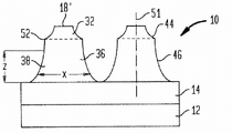
Referring now to Figure 1A to Fig. 1 C, it shows the cutaway view of each parts of the micromodule 100 that encapsulates shown in Fig. 2.As shown in the figure, the micromodule 100 of encapsulation comprises substrate 102, is facing down or the microelectronic element 104 of flip-chip position and the conductive pillar 106 that microelectronic element is engaged with substrate.Conductive pillar is included in conductive salient point or protruded stigma 108 outstanding on the face 105 of substrate 102, and conductive salient point or the protruded stigma 110 given prominence on the face 107 of conductive salient point or protruded stigma 108 and microelectronic element 104 align.Conductive pillar 106 is set to by increasing spacing distance or the vertical range between microelectronic element 104 and the substrate 102, increase the height of the encapsulation of chip on substrate, and allow the horizontal range of center to center between the conductive pillar 106 or spacing P to reduce simultaneously.As what will describe in further detail hereinafter, the increase of distance can help to reduce the stress of conductive pillar between substrate 102 and the microelectronic element 104, can help the end to fill glue material 112(with reference to Fig. 2 A) convenient the application, and allow to use a greater variety of ends to fill glue.
With reference to Figure 1A, substrate 102 preferably includes dielectric element 102A.Dielectric element 102A has end face 101 and towards opposite bottom surface 103.Plural conductive trace 109 can be along end face or bottom surface or the two extension.Dielectric element 102A can be rigidity or flexible.Dielectric element 102 can comprise the sheet material of polyimides or other polymer.Though the thickness variable of dielectric element 102, the thickness of most typical dielectric element 102A can be up to 2 millimeters.Substrate 102 can comprise other conducting elements, as is exposed to the outer contact (not shown) of bottom surface 103.Used in this application, conducting element " is exposed to " surface of dielectric element, can be such: concordant with the surface, with respect to this surface depression or outstanding from this surface, as long as this conducting element can with contact with a mathematical point that moves to this surface perpendicular to this surperficial direction.
Trace and contact can be used, and application number is that 11/014, the 439 common openly method of transferring the possession of shown in the U.S. Patent application is made, and its disclosed content is quoted adding this paper.In the specific embodiment that illustrates, the conducting element (not shown) is positioned on the end face 101 of substrate 102.But in other embodiments, conducting element also can extend along the bottom surface 103 of substrate 102, extend or extend in the inside of substrate 102 at end face 101 and bottom surface 103.Therefore, state used in this application, first feature be arranged on second feature " on ", should not be understood that, require first feature to be positioned at the surface of this second feature.Use at this paper, microelectronic element is electrically connected with substrate via protruded stigma, and " end face " relevant with substrate and " bottom surface " should be understood to microelectronic element placement location relative with it and be correlated with, rather than gravitational frame of reference.Therefore, " end face " refers to substrate and positive adjacent surface microelectronic element, and contact such as pad, metal protruded stigma etc. expose thereon." bottom surface " refers to the substrate surface away from end face.The bottom surface typically is the surface that has the contact to expose of substrate, and this contact can engage with another element of packaged microelectronic element outside such as the terminal of circuit board.In this application, " first type surface " of substrate means " end face " of substrate.
Solid metal salient point or conduction protruded stigma 108 also extend from the end face 101 of substrate 102, to form conductive pillar 106(Fig. 2 and Fig. 2 A) first.Conduction protruded stigma 108 has end face 111 and edge surface 113, and edge surface 113 stretches out from substrate 102 end faces with wide-angle, thereby end face 101 intersections of edge surface 113 and substrate 102 form tangible angle.For example, in an embodiment shown in, the end face 101 of substrate 102 and the conduction protruded stigma 108 edge surface 113 between generated greater than 90 the degree the angle.This angle of shape according to conduction protruded stigma 108 is different.For example, cylindrical protruded stigma can have the angles of 90 degree between the end face 101 of substrate 102 and conduction protruded stigma 108.Provisional application number is 60/875,730, and the applying date is on December 19th, 2006, and name is called the U.S. Patent application of the embedded printed substrate of patch capacitor; Provisional application number is 60/964,916, and the applying date is on August 15th, 2007, and name is called multilager base plate with interconnection vias and the U.S. Patent application of manufacture method thereof; Temporary patent application number is 60/964,823, the applying date is on August 15th, 2007, and name is called the U.S. Patent application that has by the interconnection element of the gold-plated protruded stigma of making, described process and the protruded stigma of example in these temporary patent applications, its disclosed content is quoted adding this paper.For example, conduction protruded stigma 108 can be made by the etch process of describing in further detail as this paper.Alternatively, conduction protruded stigma 108 can form by electroplating technology, and wherein protruded stigma 108 passes as the opening on the dielectric layer of photoresist layer by on substrate metal layer, plated metal and forming.
The big I of conduction protruded stigma 108 changes in a significant scope, but typically, each conduction protruded stigma 108 is at least 50 microns from the height H 1 of end face 103 extensions of dielectric element 102A, and may extend to up to 300 microns.These conduction protruded stigmas 108 can have the height H 1 bigger than its diameter or width W 1.But also comparable width W1 is little for this height H 1, for example be width W 1 size at least half.
Conduction protruded stigma 108 can be made by any electric conducting material, as copper, copper alloy, gold and composition thereof.Conduction protruded stigma 108 can comprise that at least one can be by the exposing metal layer of solder.For example, protruded stigma can comprise copper, has one deck gold on the protruded stigma surface.In addition, conduction protruded stigma 108 can comprise that its fusing point of one deck at least is higher than the metal of scolder fusing point, this metal will with this solder bonds.For example, this conduction protruded stigma 108 can comprise the copper layer or be made of copper fully.
Conduction protruded stigma 108 also can have multiple difformity, comprises conical butt.What substrate 114 and the top 116 of each conduction protruded stigma 108 can be roughly circle maybe can have different shapes, as rectangle or ellipse.The substrate 114 of conduction protruded stigma 108 typically has the diameter that is about the 50-300 micron, and top 116 typically has and is about 25 microns to 200 microns diameter.Each conduction protruded stigma 108 can have the substrate 114 of contiguous dielectric substrate 102 and away from the top 116 of dielectric substrate.In addition, do not comprise any solder mask from dielectric element 102A() end face 101 count, the conduction protruded stigma height H 1 typical scope be little of 30 microns, greatly to 200 microns.
As shown in the figure, solder mask 118(Fig. 2) can be arranged on substrate 102 tops and adjacent with conduction protruded stigma 108.At refluxing stage, solder mask 118 helps to prevent that the scolder overflow from reaching at 106 bridge joints of adjacent protruded stigma.
With reference to Figure 1B, microelectronic element 104 has front 122 and the back side 124.Microelectronic element 104 is preferably encapsulation and and another element interconnection semiconductor chip or analog before.For example, this microelectronic element can be nude film (bare die).
In the website of Advanpak Solutions private limited partnership (" Advanpak "), and in the patent No. is 6681982,6592109 and 6578754 United States Patent (USP), the conduction protruded stigma that can extend from microelectronic element and analog and the example of making the method for conduction protruded stigma have been described.These patents have been transferred the possession of to Advanpak, and its disclosed content is quoted adding this paper.For example, conduction protruded stigma 110 can be made by etch process.Alternatively, conduction protruded stigma 110 can be made by plating, and wherein protruded stigma 110 forms by pass the opening plated metal that is formed on the photoresist layer at substrate metal layer.Similar with the conduction protruded stigma 108 that extends from substrate, the protruded stigma 110 that extends from microelectronic element 104 can have end face 111 and edge surface 113, edge surface 113 stretches out with the end face 122 of wide-angle from microelectronic element, thereby generates tangible angle between microelectronic element and conduction protruded stigma.
For between conduction protruded stigma 110 and microelectronic element 104, providing Metal Contact, metal layer 120 under the salient point can be set in the front 122 of microelectronic element 104.The classical group of metal layer 120 material package of becoming a useful person is drawn together titanium, titanium-tungsten, chromium under the salient point.Metal layer 120 is as the conducting metal contact that is used for conductive pillar 106 under the salient point.Use the method known in the art, also can passivation layer 119 be set in the front 122 of microelectronic element 104, passivation layer 119 is arranged under microelectronic element 104 and the salient point between the metal layer 120.
With reference to Figure 1B, Fig. 1 C and Fig. 2, the size of the conduction protruded stigma 110 that extends from microelectronic element 104 also can change in significant scope, but the most typically, the height H 2 of each conduction protruded stigma 110 is for being not less than 50 microns.Conduction protruded stigma 110 can have the height H 2 greater than its width W 2.But highly also comparable width W2 is little for this, for example be width dimensions at least half.
Conduction protruded stigma 110 is preferably made by copper or copper alloy, but also can comprise other electric conducting materials, as the composition of gold or Jin Yutong.In addition, conduction protruded stigma 110 can comprise that one deck fusing point at least is higher than the metal of scolder fusing point, this metal will with solder bonds.For example, this metal protruded stigma can comprise the copper layer or all be made of copper.
In a particular embodiment, conduction protruded stigma 110 can be columniform, thereby the diameter on the diameter of protruded stigma substrate 126 and protruded stigma top 128 about equally.In one embodiment, at the bottom of the conductive bumps base for post 126 and the diameter on top 128 be about the 30-150 micron.Each conduction protruded stigma 110 can have the substrate 126 of adjacent substrates 102 and away from the top 128 of substrate 102.Alternatively, conduction protruded stigma 110 can have various shape, as conical butt, rectangle or bar-shaped.
Coating or solder caps 130 can be attached at the top 128 of conduction protruded stigma 110 or conduction protruded stigma not with part that microelectronic element 104 contacts on.Solder caps 130 can have diameter or the width W 2 identical with conduction protruded stigma 110, thereby becomes the extension of conduction protruded stigma 110.In one example, solder caps 130 can have the height H 3 that scope is approximately 25 microns to 80 microns.
Should be understood that conduction protruded stigma 108(Figure 1A that the height H 2 of the conduction protruded stigma 110 that extends from the front 122 of microelectronic element 104 can be extended with the end face 101 from dielectric element 102A) height H 1 equate.But these highly may be selected to be different, and the height H 2 of conduction protruded stigma 110 can be below or above the height H 1 of conduction protruded stigma 108.In the example of certain illustrative, the height H 2 that the conduction protruded stigma 110 that extends from microelectronic element 104 can have is 50 microns, and the height that the conduction protruded stigma 108 that extends from substrate can have is 55 microns (Fig. 2).
For microelectronic element 104 and substrate 102 are electrically connected, the conduction protruded stigma 110 on the microelectronic element 104 must be connected with the conduction protruded stigma 108 on the substrate 102.With reference to Fig. 1 C, microelectronic element 104 upset makes that conduction protruded stigma 108 is in alignment with each other on conduction protruded stigma 110 and the substrate 102 of microelectronic element 104, and moves to approaching.Solder caps 130 on the microelectronic element 104 refluxes, so that the conduction protruded stigma 110 on the solder microelectronic element 104 and the conduction protruded stigma 108 on the substrate 102.Shown in Fig. 2 and Fig. 2 A, scolder also makes up the conductive pillar 106 that extends to substrate from microelectronic element with the exposed surface of wetting conduction protruded stigma.Be used for solder bonds, the increase of the conductive pillar 108 on microelectronic element 104 and the substrate 102,110 surface area can help to reduce the current density at seam interface.The reduction of this current density can help to reduce electromigration, and higher durability is provided.
As shown in the figure, conductive pillar 106 comprises the scolder that is electrically connected with the conduction protruded stigma.In one example, in the substrate of the conduction protruded stigma that extends from microelectronic element and spacing distance or height H from the conductive pillar that extends between the expose portion of the substrate of substrate extension, an example ranges is the 80-100 micron.
Shown in Fig. 2, Fig. 2 A, the wall 132 of conductive pillar 106 can be protruding or tubbiness, wherein the midpoint area M(of conductive pillar is the part between the conduction protruded stigma 108 of the conduction protruded stigma 110 of microelectronic element and substrate) width W that has is bigger than width W 1, the W2 near the part in the part of substrate 102 end faces 101 and microelectronic element 104 fronts 102 respectively of conductive pillar 106.
Further shown in Fig. 2 A, can on microelectronic element 104 and substrate 102, the application of known method form contact mat 117.In one embodiment, lower protruded stigma 108 from substrate 102 extensions, and lower contact mat 117 can form by etching step separately, and as open day being disclosed in the PCT International Application No. WO 2008/076428 on June 28th, 2008, its disclosed content is quoted adding this paper.For example, can utilize have metal layer at top, the three-layer metal substrate of bottom metal layers 123 and middle etch stop layer or interior metal layer 121, make conduction protruded stigma 108 and contact mat 117.In a this process, the exposed surface of three layers or more multi-layered metal structure can carry out etching according to the photoresist layer of lithographic patterning, and to form conduction protruded stigma 108, etching process stops on the interior metal layer 121 of metal structure.Interior metal layer 121 comprises one or more metals that is different from metal layer at top and bottom metal layers 123, and the intermediate metal layer with this composition does not adhere to the etchant for etching metal layer at top 123.For example, metal layer at top 123 main components of etching conduction protruded stigma 108 are copper from it, and bottom metal layers 123 also can mainly be made of copper, and intermediate metal layer 121 is mainly made by nickel.With respect to copper, nickel provides good selectivity, avoids being stained with on the nickel dam etched to form the metal level of conduction protruded stigma 108.For forming contact mat 117, can carry out another etching step according to the photoresist layer of another lithographic patterning.Protruded stigma 108 can further interconnect with other conductive features such as path 115, and path 115 can further interconnect with other conductive features (not shown).
With reference to Fig. 3, the wall 232 of conductive pillar 106 ' also can be straight, thus the width W of conductive pillar 106 ' 5 with near the width W 4 ' of substrate 102 ' end face 101 ' and near the width W 4 in the front 122 ' of microelectronic element 104 ' about equally.Be understandable that width W 4, W4 ' need not to equate.Alternatively, the wall 232 ' of conductive pillar 106 ' can be recessed (referring to Fig. 4), depends on the interval of required acquisition.
Allow between dielectric element and microelectronic element, to have higher interval height according to conductive pillar according to the present invention 106, allow to be exposed to spacing P(between each conduction protruded stigma 110 in microelectronic element 104 fronts 122 simultaneously referring to Figure 1B, Fig. 2) and the spacing P that is exposed between each conduction protruded stigmas 108 of substrate 102 end faces 101 significantly reduce.In one embodiment, spacing P can be as small as 50 microns or greatly to 200 microns.Be understandable that because arrangements that be in alignment with each other of conduction protruded stigma 108,110, the spacing P between each conduction protruded stigma 108 and each spacing P that conducts electricity between protruded stigma 110 will be for equating.
Spacing P also can be the function of conduction protruded stigma 108,110 diameter or width W 1, W2, makes that basal diameter W1, the W2 of conduction protruded stigma can be up to 75% of spacing P.In other words, the ratio of diameter W1, W2 and spacing P can be up to 3:4.For example, if spacing P is 145 microns, conduction protruded stigma 108,110 diameter W1, W2 can be up to 108 microns or spacing P 75%.
The increase of interval height has reduced the strain on the low-K dielectric material that may exist in microelectronic element.In addition, increase at interval helps to make and the minimizing of the problem of the little canonical correlation of spacing, for example electromigration or problem such as crowded.This owing to conductive pillar 106 can wetting conduction protruded stigma 108, the fact on 110 surface.
With reference to Fig. 5 to Fig. 6, show the alternative arrangement that the conductive salient point that makes on the microelectronic element engages with conductive salient point on the substrate.With reference to Fig. 5, replacement is placed on conduction protruded stigma 210 tops 228 of extending from microelectronic element 204 with solder caps 230, can be placed on solder caps 230 from the top 216 of the conduction protruded stigma 208 of substrate 202 extensions.In one embodiment, the diameter W6 of the width of solder caps 230 or diameter W5 and 208 substrates 214 of conduction protruded stigma about equally.Therefore solder caps 230 stretches out on the top 216 of the conduction protruded stigma 208 that extends from substrate 202.But in case solder reflow, conductive pillar will preferably present the profile of conductive pillar shown in Fig. 2.
With reference to Fig. 6, in another alternative arrangement, solder caps 330 can all be placed on the conduction protruded stigma 310 that extends from microelectronic element 304 and the conduction protruded stigma 308 that extends from substrate 302.Conduction protruded stigma 308,310 is placed as close to each other.Heating cause solder caps 330 reflux, wetting and be fused to conduction protruded stigma 308,310.In case reflux, it is similar with the conductive pillar 306 shown in Fig. 2 that conductive pillar 306 will be preferably.
With reference to Fig. 7, show a kind of alternative arrangement of microelectronics Packaging.Layout shown in this layout and Fig. 2 is similar, and difference only is to have lacked the solder mask contiguous with the conduction protruded stigma that extends from substrate.In layout that this substitutes, can use path 307 so that conductive pillar 406 be exposed to substrate 402 bottom surfaces namely the circuit (not shown) on the face relative with the end face 401 of substrate 402 be electrically connected.Use path 307 and eliminated the demand of solder mask.
With reference to Fig. 8, show alternate embodiment, the combination (metal to metal bond) of metal and metal of wherein conducting electricity between the protruded stigma does not have application of solder and forms.And change into, the combination between the conduction protruded stigma 508,510 can being out of shape is engaged with each other forms by making it.Conduction protruded stigma 508,510 is preferably made by elasticity or the minimum extensible material of resilience, as being pure gold substantially.And conduction protruded stigma 508,510 can combine by congruent melting bonding between protruded stigma and cladding material (eutectic bonding) or anode linkage (anodic bonding).For example, conduction protruded stigma 508,510 top 516,517 can cover a spot of tin, silicon, germanium or other materials, and these materials can form the relative low alloy of fusing point with gold.Protruded stigma can all be made of gold or have gold plating on its surface.In the be engaged with each other back heating of conduction protruded stigma 508,510, spread between the material of conduction protruded stigma 508,510 material and conductive bumps capital end 516, the interface formation fusing point between protruded stigma and wall is lower than the alloy of individual element fusing point.When assembly remained on high temperature, further diffusion caused in a large amount of gold of alloying element from interfacial diffusion to protruded stigma, thereby the fusing point of material improves at the interface, causes the interface to be solidified, and formed firmly to connect between two parts.
With reference to Fig. 9, it is consistent with Fig. 8, preferably all is made up of copper and directly fusion each other except conduction protruded stigma 608,610, does not have between the conduction protruded stigma beyond low-melting-point metal such as scolder or the tin existence.Preferably, be to obtain strong bonded, at conduction protruded stigma 608,610 with before terminal engages, conduct electricity protruded stigma 608,610 composition surface must be clean and do not have oxide substantially, as native oxide (native oxides).Typically, can be characterized as the process of surface treatment of etching or microetch to remove the oxide on surface as the noble metal of copper, nickel, aluminium and other metals, this surface etching technology does not influence salient point or its below metal layer thickness substantially.This cleaning process is preferably in actual engagement and crosses the Cheng Qian and carry out in very short time.Each parts after the cleaning remain on the following time of condition that relative humidity is percent 30 to 70 normal humidity environment, cleaning process can be carried out before several hours at engaging process usually, before six hours, can not influence the intensity of the combination that generates between salient point and the capacitor terminal.
To shown in Figure 11, when conduction protruded stigma 608,610 engaging process carry out, place spacer structures 726 at the end face 601 of substrate 602 as Figure 10.Spacer structure 626 can be made by one or more materials, as polyimides, pottery or as one or more metals such as copper.The microelectronic element 604 that has conduction protruded stigma 610 to extend on it is placed on spacer structure 626 tops, makes the top 628 of conduction protruded stigma 610 of microelectronic element 604 cover the top 616 of the conduction protruded stigma 608 of substrate 602.With reference to Figure 10, spacer structure 626, microelectronic element 604 and substrate 602 are inserted between a pair of plate 640, and heating also simultaneously applies pressure to the conduction protruded stigma with the direction shown in the arrow 636.As shown in Figure 9, the pressure that is applied to plate 640 have make conduction protruded stigma height minus little effect, the height H 6 of the conduction protruded stigma after exerting pressure be lower than the conduction protruded stigma 608 of the most initial manufacturing, elemental height H5(Figure 10 of 610).An example ranges of exerting pressure in this step is between about 150kg/cm2 at about 20kg/cm2.Engaging process is for example to carry out between about 140 degrees centigrade to about 500 degrees centigrade in temperature range.
In engaging process, the compression conductive protruded stigma makes the metal under conduction protruded stigma 608,610 the previous end face begin contact and adds in heating depresses joint.As the result of engaging process, conduction protruded stigma 608,610 height can reduce by 1 micron or more.When conduction protruded stigma 608, when 610 main component is copper, the contact between the conduction protruded stigma also mainly is made up of copper, so has formed the continuous steel structure that comprises salient point and terminal.Thereafter, as shown in Figure 9, remove plate and spacer structure, remaining sub-component 250 has the conductive pillar 606 that is formed by conduction protruded stigma 608,610 electrical connector.
With reference to Figure 12, show according to another kind of alternate embodiment of the present invention.Difference only is, replaces single layer substrate, can use multilager base plate.Application No. is 60/964,823, and the applying date is on August 15th, 2007, and name is called the patent application with interconnection element of electroplating the protruded stigma that forms; Application No. is 60/964,916, and the applying date is on August 15th, 2007, and name is called multilager base plate with interconnection vias and the patent application of manufacture method thereof; Application No. is 11/824,484, the applying date is on June 29th, 2007, and name is called the patent application of the multilayer wiring element with pin interface, multilager base plate described in multilager base plate such as these U.S. Patent application documents, its disclosed content is quoted adding this paper.As shown in the figure, multilager base plate 702 and microelectronic element 704 engage with flip chip, and microelectronic element 704 can be as having the semiconductor chip of active device, passive device or active and passive device.From the top 716 of the outstanding conduction protruded stigma 710 of the end face 701 of multilager base plate, with 710 as described herein connections of conduction protruded stigma of extending from microelectronic element.As shown in the figure, the conduction protruded stigma 708 of multilager base plate 702 can directly engage with the conduction protruded stigma 710 from the positive extension of microelectronic element, handle the metal (finished metal) that forms as for example gold by on protruded stigma top 160 etc., and another kind is present between the metal in conductive pad and the protruded stigma diffusion interlinked (diffusion bond).Alternatively, conduction protruded stigma 708,710 can be bonded together by fusible metal such as scolder, tin or eutectic composition, and the wetting protruded stigma of fusible metal and pad are to form contact wetting or welding.For example, the form that fusible metal can the solder bump (not shown) provides, and is exposed on the front 722 of microelectronic element 704, and solder bump is arranged on a side of conductive bumps capital end or both sides' end.
Conductive pillar also can utilize in stacked package, for example in the following application of owning together: Application No. is 60/963,209, the applying date is on August 3rd, 2007, name is called, and has the patent application of the die stack encapsulation of making in wafer scale of constructing wafer element again of application extension pad; Application No. is 60/964,069, and the applying date is on August 9th, 2007, and name is called, and has the patent application of the crystal circular piled encapsulation of selecting single chip for use; Application No. is 60/962,200, and the applying date is on July 27th, 2007, and name is called, and adds the patent application of constructing the stacked wafer encapsulation again of expansion pad after having; Reaching Application No. is 60/936,617, and the applying date is on June 20th, 2007, and name is called constructs crystal circular piled patent application again.
For example, with reference to Figure 13, in an alternative embodiment, the package assembling that piles up comprises first sub-component 800 and second sub-component 802.The microelectronic element of first sub-component and second sub-component and encapsulation shown in Figure 2 is basic identical, except substrate 806,806 ' further stretches out to be contained in the conductive pillar 808 that extends between the substrate 806,806 ' of first sub-component and second sub-component.Conductive pillar 808 also comprises the conduction protruded stigma 812 that extends and be connected with the path 814 that passes the extension of the second sub-component substrate top surface and bottom surface from substrate.
Figure 14 is the structural representation of three-layer metal substrate 10.Three-layer metal substrate 10 has trace layer 12, etching stopping layer 14, thick-layer 16 and end face 18.Trace layer 12 can be made of such as copper by easy etched first metal with thick-layer 16, and etching stopping layer can be made by the metal as nickel, and nickel is anti-etching in the process that is used for etch copper substantially.But copper and mickel is exemplary, and substrate 10 can be made by any suitable material as required.
Figure 15 is the structural representation of the three-layer metal substrate 10 among Figure 14 when having first photoresist 20.First photoresist 20 is deposited on the end face 18.First photoresist 20 can be any type, when being exposed to the material that can harden or carry out chemical reaction under radiation such as the light.Therefore, corrosion resistant material all can be used arbitrarily.Well known in the prior art, positive photoresist and negative photoresist also all can utilize.
Figure 16 is the structural representation when the three-layer metal substrate has first photoresist 20 and mask 22 among Figure 14.Mask 22 is generally the transparent panel with printing zone of opacity thereon; be called photomask or shadow mask; the pattern 24 that generates at mask 22 has, and the zone that the mask 22 of being indicated by label 26 covers reaches the zone that does not have masked covering by label 28 indications.Pattern 24 with overlay area 26 and uncovered area 28 optionally allows first photoresist 20 of part to be exposed under the radiation respectively.
In case mask 22 is placed on the top of first photoresist, just begins to provide radiation.The most frequently used radiation is with ultraviolet form.This radiant exposure is at first photoresist 20 of uncovered area 28, and it is insoluble that the result becomes uncovered area 28.Situation is opposite when using negative photoresist, and overlay area 26 becomes insoluble.Behind exposure first photoresist 20, remove mask 22.With 20 flushings (developed) of first photoresist, solution is removed first photoresist that does not become insoluble position in first photoresist by cleaning with solution then.Therefore, the exposure of photoresist and flushing make the pattern that forms insoluble material at the end face 18 of substrate 10.The pattern 24 of this pattern reflection mask 22 of insoluble material.
After photoresist exposure and flushing (development), etching substrates as shown in figure 17.In case after reaching specific etch depth, etching process interrupts.For example, etching process can finish in a scheduled time.Etching process stays the first microcontact part 32 that projects upwards from substrate 10 at thick-layer 16.When etchant etch thick-layer 16, it removes the material of below, first photoresist, 20 edges, allows first photoresist 20 laterally projecting from the top of microcontact part 32, is designated as the portion of dangling 30.First photoresist 20 remains on the ad-hoc location of being determined by mask 22.
In case after thick-layer 16 is etched to desired depth, just depositing second layer photoresist 34(Figure 18 at three-layer metal substrate 10).In this case, second photoresist 34 etched position before thick-layer 16 deposits.Therefore, second photoresist 34 also covers the first microcontact part 32.If photic anti-dose of using electrophoresis, because its intrinsic chemical characteristic, second photoresist 34 can not be deposited on first photoresist 20.
In step next, the substrate with first photoresist 20 and second photoresist 34 exposes under radiation, washes second photoresist then.As shown in figure 19, first photoresist 20 is laterally projecting on the part of thick-layer 16, is designated as the portion of dangling 30.This portion 30 of dangling prevents that second photoresist 34 from exposing under radiation, therefore, prevent that it is rinsed and removes, and makes the part of second photoresist 34 stick on the first microcontact part 32.Therefore, the mask that act as second photoresist 34 of first photoresist 20.Second photoresist 34 washes to remove second photoresist 34 that exposes under radiation by cleaning.Stay the unexposed portion of second photoresist 34 like this in the first microcontact part 32.
After in case the part of second photoresist 34 is exposed and washes, just can carry out second etching process, remove the other part of the thick-layer 16 of three-layer metal substrate 10, thereby below the first microcontact part 32, form the second microcontact part 36, as shown in figure 20.In this step, second photoresist 34 still sticks on the first microcontact part 32, protects the first microcontact part 32 not by etching again.
These steps can be repeated required number of times arbitrarily, to form the 3rd, the 4th or n microcontact part, make up preferred depth-width ratio and spacing.This process can stop when arriving etching stopping layer 14.As last step, first causes resist 20 and second photoresist 34, can be peeled off fully respectively.
The microcontact 38 that these processes generate is shown in Figure 21 A to Figure 21 D.These figure also show and use the obtainable various profiles of process described herein.With reference to Figure 21 A to Figure 21 C, microcontact 38 has the first 32 of the top area of being also referred to as, and is also referred to as the second portion 36 of bottom section.If the first photoresist sheet of using in step mentioned above is circular, each microcontact will be generally with around central shaft 51(Figure 21 A) the form of rotary body upwards extend with vertical direction or Z-direction from the remainder of substrate, and generally perpendicular to the plane, place of etching stopping layer 14.The width of first and second portion or diameter X in each part along the position of Z-direction or short transverse and change.In other words, in first, X=F1(Z), and in second portion, X=F2(Z).52 places, border between first and second parts, gradient or dX/dZ can sharply change.In each part, gradient or dX/dZ sharply do not change along the position of Z-direction usually, therefore, can not produce step and change.In each part, typically along the position of Z-direction, it is stepping that gradient or dX/dZ change.
Further shown in Figure 21 A, the outer peripheral face 44 of the first 32 in microcontact zone and the outer peripheral face 46 of second portion 38 are recessed surfaces, and each outer peripheral face has gradient or the dX/dZ that gradually changes along the Z-direction position.Each outer peripheral face (for example surface 44 or surperficial 46(Figure 21 A) about microcontact described herein), " depression " refer between the border of outer peripheral face each the height (as, each height 29(Figure 21 E between the lower boundary 52 of the coboundary 19 of outer peripheral face 44 and outer peripheral face 44)), the diameter 25 that outer peripheral face impales, less than equal height 29 times, by the diameter that theoretical taper seat impales, theoretical taper seat is determined by a series of straight lines that extend between the border.For example, each point on the outer peripheral face 44 between border 19,52 all is positioned at the inside of passing the theoretical taper seat 48 that a series of straight lines of extending on border 19,52 determine.
The specific function of microcontact and the profile that therefore has thereof are determined by the etching condition of using in first etching step and second etching step.For example, the composition of etchant and etch temperature can change, to change the speed of etchant etch metal level.Etchant also can change with the means that contact of metal level.Etchant can force sprinkling or substrate to immerse in the etchant to substrate.During first and second portion etching, etching condition can be identical or different.
In the microcontact shown in Figure 21 A, the outer peripheral face 44 of each first 32 and the outer peripheral face 46 of second portion 36 are recessed.In addition, in the embodiment of Figure 21 A, the outer peripheral face 44 that first 32 has outwards opens with direction down, thereby the value of gradient or dX/dZ increases with down direction.Second portion 36 also has outside open outer peripheral face 46; 52 places on the border, the gradient of second portion or the value of dX/dZ are minimum value, and increase gradually along the direction towards the protruded stigma substrate.52 place's gradients have change in fact on the border.In microcontact and layer 14 substrate that engages, second portion has Breadth Maximum or diameter X, and the Breadth Maximum of second portion or diameter X are in fact greater than first's Breadth Maximum or diameter.
Among each embodiment that sees in Figure 21 A to Figure 21 D, the outer peripheral face of each part of each microcontact is recessed.These embodiment otherwise change.For example, in Figure 21 B, the Breadth Maximum of second portion 36 only than the Breadth Maximum of first 32 slightly more greatly.And in the substrate of protruded stigma and a certain position between the border 52, second portion has minimum widith, thereby width is decreased to minimum gradually in the upward direction, increases to border 52 more in the upward direction gradually from minimum then.This shape is commonly referred to " cooling tower " shape.In the microcontact of Figure 21 B, gradient or the dX/dZ border 52 place's reindexing (sign) between two parts.In Figure 21 C, second portion 36 has its minimum widith near the microcontact substrate.
At last, Figure 21 D shows and has two with the profile of the microcontact on top.Such profile can have been carried out situation for several times and caused by the several steps in the process described herein.Therefore, this specific microcontact 38 has four parts as can be seen, is respectively first 32, second portion 36, third part 40 and the 4th part 42.These four parts can have size arbitrarily, and comparable another part is wideer or narrower when needed.In this example, can have the border above.Be representational profile among Figure 21 A to 21D, various profiles all can obtain.First 32 also can be described as top area, and the 4th part 42 also can be described as bottom section, and second portion 36 and third part 40 can be described as zone line.
Although in each of Figure 21 A to Figure 21 D, only described the arrangement that comprises two microcontacts or protruded stigma, in fact, can form the protruded stigma array that comprises many protruded stigmas.Among each embodiment that describes in Figure 21 A to 21D, all microcontacts or protruded stigma are by single metal level 16(Figure 27 in the arrangement) make.In the substrate of microcontact, each microcontact covers the part of etching stopping layer 14, and microcontact is connected with metal level 12.As will be hereinafter described, etching stopping layer 14 be removed in the zone between microcontact usually, and etched or other modes of metal level 12 handle to be converted into trace or other conductive features that is connected with microcontact usually.But, on the main body of each microcontact, be monolithic entity from its substrate to its top, do not have contact such as solder joint, and entire body has basic composition uniformly.And, because in the end away from the microcontact of layer 12 and 14, the top end surface 18 ' of microcontact is metal level 16(Figure 14) the part of initial end face 18, these top end surface substantially flat and levels, and the top end surface of all microcontacts top end surfaces basic and other microcontacts are coplanar.
In alternate embodiment, behind first etching step, not only to remove first photoresist 20 in selected position, the first whole photoresists 20 can all be removed.In this case, second photoresist 34 can be at the whole surface deposition of substrate 10.Place mask 22 at second photoresist 34 then.Mask 22 is alignment accurately, and feasible position of only formerly exposing is in 32 exposures of the first microcontact part.Wash second photoresist 34 then, and can carry out further etching at substrate 10.
Figure 22 is the flow chart of describing first embodiment.With step 1100 beginning, provide substrate.Then when step 1102, at substrate deposition photoresist n.When step 1104, place mask on photoresist n top then.When step 1106, exposure photoresist n under radiation.Subsequently, when step 1108, remove mask, then when step 1110, at selected position flushing photoresist n and etching substrates.
Next, when step 1112, deposit another photoresist that is called as n+1.Then, when step 1114, this photoresist n+1 exposes under radiation.Subsequently, when step 1116, remove photoresist n+1, etching substrates again at select location.Then, when step 1118, judge whether the microcontact height that reached required.If do not obtain required microcontact height, then when step 1120, process is back to step 1112, at another photoresist of substrate deposition.If when step 1122, obtained required height, remove residual photoresist in step 1124 then, process is finished.
Figure 23 is the flow chart of describing second embodiment.The step 1200 of second embodiment copies step 1100 among first embodiment to 1110 to 1210.But, when step 1212, remove whole photoresist n.Then, when step 1214, at another layer of substrate deposition photoresist n+1.Next, mask is put back on the substrate when step 1216.In this step, mask must align, and makes its pattern be placed on substantially and the same position of mask when photoresist n places.Subsequently, when step 1218, exposure photoresist n+1 removes mask then under radiation.
Next, when step 1220, optionally remove photoresist n+1, and etching substrates again.This process also can repeat, up to obtaining required microcontact height.Therefore, when step 1222, judge whether the microcontact height that reaches required.If do not reach preferred height when step 1224, then this process is got back to step 1212, and photoresist is removed fully, and deposits another photoresist n+1, and step continues at this point.But, if when step 1224, reached required height, when step 1228, remove remaining photoresist, this process finishes.
Etching stopping layer 14 and thin layer 12 can be bonding with a dielectric layer, and thin layer 12 can be etched with the formation trace then, thereby provide, and has the microcontact that is connected with trace and reach from the parts of the outstanding microcontact of dielectric layer.Such structure can be applicable to, for example, and as an element of semiconductor die package.For example, can be 11/318822 in Application No., the applying date is to use in the U.S. Patent application on December 27th, 2005, its disclosed content is quoted adding this paper.
Structure described herein can be multilager base plate 10 part of the whole, for example, as shown in figure 24, the top layer of multilager base plate 10.Microcontact 38 can weld with nude film 54.Scolder 56 can soak into the part of (wick) microcontact 38.Soak into (wicking) good contact the between microcontact 38 and the nude film 54 is provided.Except scolder 56, also can use other combined process.What center on microcontact 38 is to fill glue 58 end, is used for nude film 54 is bonded in microcontact 38 and substrate 10.As long as need, fill glue 58 and all can use at the end of any type, maybe can save the end and fill glue 58.Microcontact 38 belows are trace 60 and dielectric layer 62.Terminal 64 is positioned at the bottom of substrate 10.
Specific encapsulation comprises the microelectronic chip that piles up.This makes and is encapsulated in surface area occupied on the substrate, less than the total surface area of piling up chips.The encapsulation that comprises the microcontact of using process manufacturing described herein can be piled up.Can be 11/140312 with reference to the Application No. of while pending trial, the applying date is the U.S. Patent application on May 27th, 2005; And U.S. Patent number is 6782610 United States Patent (USP), and its disclosed content is quoted adding this paper.The etching step of the microcontact of instructing in these open texts can substitute with process described herein.
Although above-described is the three-layer metal substrate, however the suitable substrate with any number of layers all can utilize, for example, single metal plate.In addition, do not adopt photoresist, can adopt corrosion resistant material such as gold, or when the etching thick metal layers, resist other metals of used etchant corrosion substantially.For example, can adopt corrosion resistant metal to replace the first above-mentioned photoresist 20.After using the mask as photoresist, mask has the hole that holds the corrosion resistant metal sheet in desired location, and the corrosion resistant metal sheet can be plated out on the top of thick-layer 16.After corrosion resistant metal is electroplated at the thick-layer top, but the etching thick-layer is to form microcontact mentioned above.Corrosion resistant metal can be stayed the top of microcontact.Under the situation that corrosion resistant metal is used as second corrosion resistant material (replacing the second above-mentioned photoresist 34), masks may limits the deposition of second corrosion resistant metal, make it only to be deposited in the first 32 of microcontact, thereby the zone between the microcontact keeps not having corrosion resistant metal.Alternatively, after the etching first microcontact part 32, whole ground floor corrosion resistant metals can be removed, second layer corrosion resistant metal can be deposited then to protect the first microcontact part 32.
With reference to Figure 25, show the microelectronic unit 70 with microcontact 72.Microcontact 72 has etching stopping layer 74.Microcontact 72 is vertically outstanding from metal level, and metal level has become trace 76.Between trace 76, can have gap or space 78.But first dielectric layer, 80 adjacent trace 76 stick to the bottom side of unit 70.Opening 82 on first dielectric layer 80 allows trace 76 to become electric contact.Second dielectric layer 84 can be formed on the top side of unit 70.
By the microcontact that these processes form, the exemplary height scope that can have is from about 40 microns to about 200 microns.Further, the typical pitch between the microcontact can be less than 200 microns, preferably less than 150 microns.Especially, with reference to Figure 26, two microcontacts that illustrate have top end diameter d and microcontact height h.Spacing P is determined by the distance between the longitudinal axis of two microcontacts.
In a lot of the application, particularly when microcontact was applied to be connected with the contact of semiconductor chip, for example, in the structure that reference Figure 27 will be described below, it was desirable that little spacing is provided.But the technology that microcontact forms by single etch process from single metal level, making spacing P usually is unpractiaca less than specific minimum spacing P0.P0 and diameter d add height h's and equate, that is, and P0=d+h.In theory, minimum spacing can reduce by reducing top end diameter d.But making top end diameter is impossible less than zero.In addition, making top end diameter be decreased to about in many cases is unsuitable below 20 or 30 microns.For example, top, contact and be used for adhesion between the photoresist sheet on etching process protection top is proportional with the area on top, therefore square proportional with top end diameter.Therefore, under the very little situation of top end diameter, the photoresist sheet can shift out original position during the course.Thereby, use traditional technology, be difficult to formation and have very closely spaced microcontact.
But, use process described herein, the spacing of microcontact can be less than P0, (P<P0), for example, P=(0.9) P0 or littler.For example, if the diameter d on top is 30 microns, height h is 60 microns, and it is 90 microns minimum spacing P0 that conventional process will obtain.But, in process described herein, using at least twice etching process, obtainable spacing P is about 80 microns or littler.In other words, multistage etching process allows, and from single metal microcontact or the protruded stigma that single metal level forms, has the combination of unreachable spacing, top end diameter and height in conventional etching process.Along with the increase of etching progression, given top end diameter and highly obtainable minimum spacing reduce.
Referring now to Figure 27, show microelectronics Packaging 90, it has used potted element or the chip carrier with above-mentioned microcontact 38.Chip carrier comprises first dielectric layer 62, and it can be made by the dielectric material that polyimides, BT resin or other are generally used for making chip carrier.Chip carrier also comprises the trace 60 that is connected with some or all of microcontacts 38.Trace and terminal 61 merge.As shown in figure 27, microcontact 38 is from first side of dielectric layer 62, towards last outstanding.Dielectric layer 62 has opening 82, and terminal 61 is exposed to second side, or exposes in the face of the surface of first dielectric layer 62 downwards by opening 82.Carrier further comprises available second dielectric layer 84.
The top of microcontact 38 and 55 combinations of the contact of microelectronic element, microelectronic element such as semiconductor chip or nude film 54.For example, the top of microcontact can with contact 55 seam of microelectronic element.Also can use other combined process, as congruent melting bonding or diffusion combination.The packaged microelectronic element of gained, some or all contacts 55 on its microelectronic element by microcontact and trace, are connected with terminal 61.The microelectronic element of encapsulation can pass through the combination of the pad 94 on terminal 61 and the circuit board 92, and is mounted to circuit board 92, on printed circuit board (PCB).For example, at opening 82 application of solder balls 96, the pad 94 on the circuit board 92 can weld with terminal 61.
Even when closely arranging in the contact, the connection between the contact 55 of microcontact 38 and microelectronic element still can provide reliable connection.As mentioned above, microcontact 38 can form and have tangible top end diameter and height.Suitable top end diameter can be provided at sufficient calmodulin binding domain CaM is provided between the contact of each microcontact and microelectronic element.In use, chip 54 is with respect to the difference of thermal expansion and the contraction of circuit board 92, and the crooked and inclination of available microcontact 38 is regulated.This effect is strengthened with the increase of microcontact height.In addition, because microcontact forms by common metal level, in the very accurate margin of tolerance, the height of microcontact is homogeneous.Made things convenient for engaging between the contact of microcontact top and chip or other microelectronic elements like this, and the formation of strong bonded.
The structure of chip carrier is changeable.For example chip carrier can include only one dielectric layer.Trace can be positioned at the either side of dielectric layer.Alternatively, chip carrier can comprise multilayer dielectric layer, and can comprise the multilayer trace, and other features, as the conductive earthing face.
The process of the further embodiment of the present invention is used the structure (Figure 28) with protruded stigma part 1550, and protruded stigma 1550 is from surface 1526, and is outstanding as the surface of dielectric layer 1510.Protruded stigma part 1550 can form by arbitrary process, but preferably to form with similar etching process mentioned above.After protruded stigma part 1550 forms, apply metal or other conductive layers 1502 on the top 1533 of protruded stigma part 1550.For example, layer 1502 can be laminated on the structure that is associated with protruded stigma part 1550, and with the top metallurgical binding (metallurgically bonded) of protruded stigma part 1550.Optionally processing layer 1502, feasible removing away from the material on the layer of protruded stigma part 1550, but stay the layer of the segment thickness that covers protruded stigma part 1550 at least, thereby form the additional protruded stigma part 1504(Figure 29 that aligns with protruded stigma part 1550), therefore form compound microcontact, each comprises one near the base portion post part 1550 of substrate and away from the tip post part 1504 of substrate, tip post part vertically or Z-direction partly outstanding from the base portion post.Processing to layer 1502 can comprise etching process as indicated above, uses the corrosion resistant material sheet 1506 that aligns with protruded stigma part 1550.Before etch layer 1502, can use protective layer such as dielectric sealant 1508 to cover protruded stigma part 1550.Alternatively or additionally, before etch layer 1502, protruded stigma part 1550 can be with electroplating or additive method covers anti-corrosion electric conducting material, as nickel or gold.
The process that makes up follow-up protruded stigma part can repeat, so that form extention in additional protruded stigma part 1504, thus microcontact can form random length substantially.Long microcontact improves flexibility, and the amount of movement on protruded stigma top increases.One or more layers dielectric sealant can be stayed the position around established protruded stigma part, and as the layer 1508 among Figure 28 and Figure 29, it is soft that sealant is preferably, thereby it does not limit the bending of protruded stigma substantially.In other embodiments, sealant can be removed before parts use.Although microcontact be similar to dielectric substrate mentioned above 1522 and trace 1528 in conjunction with and describe, this process can be used for basically making microcontact in structure arbitrarily.
As shown in figure 29, each microcontact has along the vertical direction of base portion post part 1550 or Z-direction scope and the level or the width dimensions X that change, and the contact between base portion post part 1550 and tip post part 1504, the level of microcontact or width dimensions X sharply increase in the mode that is roughly step, and in the vertical scope of tip post part, the level of microcontact or width dimensions X vertically change.Contact between the protruded stigma each several part, width also is sharply to change to the variation of the gradient of vertical position.In each post part, the pattern that level or width dimensions change is according to deciding for etching or other processes that forms this protruded stigma part.For example, in a further embodiment, tip post part 1504 can be formed by multi-stage etching process as indicated above, thereby each tip post partly comprises different subdivisions, the function that different subdivisions has different Fixed width degree X really vertically or Z-direction changes.
Also with reference to following document, and quote adding this paper: U.S. Patent application: application number is 10/985126, and the applying date is on November 10th, 2004; Application number is 11/318822, and the applying date is on December 27th, 2005; Application number is 11/318164, and the applying date is on December 23rd, 2005; Application number is 11/166982, and the applying date is on June 24th, 2005; Application number is 11/140312, and the applying date is on May 27th, 2005; And the patent No. is 7176043 United States Patent (USP).
Being used to form the process of the applied protruded stigma of this paper, can be described in 11/717,587 the U.S. Patent application as application number, and its disclosed content is quoted adding this paper.
Referring now to Figure 30, it shows the cutaway view of the micromodule 900 of encapsulation, the micromodule 900 of encapsulation be with reference to shown in Figure 1A to Fig. 2 A and in the change example of above-described assembly, wherein from the protruded stigma 916 of the front extension of microelectronic element 902, comprises the conduction protruded stigma of multiple etching.
As shown in the figure, in this became example, the micromodule 900 of encapsulation comprised substrate 901, and substrate is shown in Figure 1A and above with reference to as described in Figure 1A.This assembly also comprises, facing down or the microelectronic element 902 of flip-chip position, and the conductive pillar 903 that substrate is engaged with microelectronic element.Conductive pillar 903 is included in conductive salient point or protruded stigma 912 outstanding on the first type surface 906 of substrate 901, and conductive salient point or protruded stigma 912 align with conductive salient point or the protruded stigma 916 given prominence to from the front 909 of microelectronic element 902.
As shown in figure 30, conductive pillar 903 comprises the scolder of interconnect conductive protruded stigma 912 conductively and 916, thereby has made up the conductive pillar 903 that extends to substrate 901 from microelectronic element 902.Conductive pillar 903 can be by with reference to other embodiment of this paper and the combination of disclosed arbitrary process, material or material and combination.For example, conductive pillar 903 can combine by congruent melting bonding or anode linkage between protruded stigma and cladding material.
More specifically, the protruded stigma 912 that extends from substrate 901 can be the protruded stigma 108 shown in Figure 1A, Fig. 1 C, Fig. 2 and Fig. 2 A, thereby the protruded stigma 916 that extends from microelectronic element 902 can replace corresponding protruded stigma 110, and each protruded stigma can comprise solder caps 130.
With before protruded stigma 916 engages, protruded stigma 912 can be the protruded stigma 208 shown in Fig. 5 at protruded stigma 912, and each comprises solder caps 230, thereby protruded stigma 916 can replace corresponding protruded stigma 210.Protruded stigma 912 can be the protruded stigma 308 shown in Fig. 6, and each comprises solder caps 330, thereby protruded stigma 916 can replace corresponding protruded stigma 310, and each protruded stigma also can comprise solder caps 330.
In certain embodiments, protruded stigma 912 can be the protruded stigma 508 shown in Fig. 8, thereby protruded stigma 916 can replace corresponding protruded stigma 510.In such embodiments, protruded stigma 912 and 916 is preferably made by elasticity or the minimum ductile material of resilience, and as be pure gold substantially, each protruded stigma setting is deformable, with corresponding protruded stigma joint, and need not application of solder.
(not shown) in other embodiments, protruded stigma 916 can be the conduction protruded stigma of any multiple etching, for example comprises the microcontact 38 of the multiple etching shown in Figure 21 A, Figure 21 C and Figure 21 D.Although by dual etched, protruded stigma 916 can surpass twice etching at the protruded stigma 916 shown in Figure 30, four etchings as shown in Figure 21 D.
Referring now to Figure 31, it shows the cutaway view of the micromodule 920 of encapsulation, the micromodule 920 of encapsulation is the change example that reaches shown in Figure 1A to Fig. 2 A above with reference to the described assembly of Figure 1A to Fig. 2 A, the protruded stigma 932 that extends from the end face of substrate 921 wherein comprises the conduction protruded stigma of multiple etching.
The micromodule 920 of encapsulation shown in Figure 31 is basic identical with encapsulation microelectron assembly 900 shown in Figure 30, except the protruded stigma 932 that extends from substrate 921 is the multiple etching protruded stigma, the dual etched microcontact 38 of protruded stigma 932 shown in Figure 21 B, and can be the conduction protruded stigma of any type from the protruded stigma 936 that microelectronic element 922 extends, comprise with reference to other embodiment of this paper and the conduction protruded stigma of disclosed any type.
As shown in the figure, in this became example, encapsulation microelectron assembly 920 comprised shown in Figure 1A and above with reference to the described substrate 921 of Figure 1A.This assembly also is included in and faces down or the microelectronic element 922 of flip-chip position, and the conductive pillar 923 that substrate is engaged with microelectronic element.Conductive pillar 923 is included in conductive salient point or protruded stigma 932 outstanding on substrate 921 first type surfaces 926, and conductive salient point or protruded stigma 932 align with conductive salient point or the protruded stigma 936 given prominence in the front 929 of microelectronic element 922.
As shown in figure 31, conductive pillar 923 comprises the scolder of interconnect conductive protruded stigma 932 conductively and 936, thereby has made up the conductive pillar 923 that extends to substrate 921 from microelectronic element 922.Conductive pillar 923 can the combination of disclosed arbitrary process, material or material combines by other embodiment of reference this paper.
More specifically, the protruded stigma 936 that extends from microelectronic element 922 can be the protruded stigma 110 shown in Figure 1B, Fig. 2 and Fig. 2 A, thereby the protruded stigma 932 that extends from substrate 921 can replace corresponding protruded stigma 108.Each can comprise solder caps 130 in the protruded stigma 936.
With before protruded stigma 932 engages, protruded stigma 936 can be the protruded stigma 210 shown in Fig. 5 at protruded stigma 936, thereby protruded stigma 932 can replace the corresponding protruded stigma that comprises solder caps 230 208.Protruded stigma 936 can be the protruded stigma 310 shown in Fig. 6, and each comprises solder caps 330, thereby protruded stigma 932 can replace corresponding protruded stigma 308, and each protruded stigma also comprises solder caps 330.
In a particular embodiment, protruded stigma 936 can be the protruded stigma 510 shown in Fig. 8, thereby protruded stigma 932 can replace corresponding protruded stigma 508.In such embodiments, protruded stigma 932 and 936 is preferably made by elasticity or the minimum extensible material of resilience, and as be pure gold substantially, each protruded stigma is set to deformable, with corresponding protruded stigma joint, and need not application of solder.
Referring now to Figure 32, it shows the cutaway view that piles up micromodule 940, pile up micromodule 940 for reaching the change example above with reference to the described assembly of Figure 1A to Fig. 2 A shown in Figure 1A to Fig. 2 A, wherein protruded stigma 952 extends from the end face of substrate 941, from the protruded stigma 956 that extend in the front of microelectronic element 941, comprise the conduction protruded stigma of multiple etching.
As shown in the figure, in this became example, the micromodule 940 of encapsulation comprised shown in Figure 1A and above with reference to the described substrate 941 of Figure 1A.Assembly also is included in and faces down or the microelectronic element 942 of the chip position of falling the shape, and the conductive pillar 943 that substrate is engaged with microelectronic element.Conductive pillar 943 is included in salient point or the protruded stigma of giving prominence on the first type surface 946 of substrate 941 952, and salient point or protruded stigma 952 align with salient point or the protruded stigma 956 given prominence to from the front 949 of microelectronic element 942.
Shown in figure 32, conductive pillar 943 comprises the scolder with conduction protruded stigma 952 and 956 conductive interconnections, thereby has made up the conductive pillar 943 that extends to substrate 941 from microelectronic element 942.Conductive pillar 943 can the combination of disclosed arbitrary process, material or material combines by other embodiment of reference this paper.
Although shown protruded stigma 952 is all identical with the dual etched microcontact 38 shown in Figure 21 B with 956, (not shown) in other embodiments, protruded stigma 952 can have the multiple etching shape different with protruded stigma 956, comprise, for example, protruded stigma 952 can be shape shown in Figure 21 A, protruded stigma 956 can be the shape shown in Figure 21 C, determine that first function of protruded stigma 952 profiles and second function determined by the etching condition of using in first etching of protruded stigma 952 and second etching step, determine the 3rd function of protruded stigma 956 profiles and the 4th function by applied etching condition in first etching of protruded stigma 956 and second etching step and determine that first function can be different with the 4th function with the 3rd function with second function.
Although protruded stigma shown in Figure 32 952 and 956 is dual etched, the arbitrary or both in the protruded stigma 952 and 956 can surpass twice etching, four etchings as shown in Figure 21 D.Protruded stigma 952 and 956 can be the compound microcontact with structure shown in Figure 28 and 29, and wherein each protruded stigma 952 and 956 comprises, the tip post part 1504 that the base portion post part 1550 of adjacent substrates 942 reaches away from substrate.
More specifically, arbitrary or both can comprise solder caps in the protruded stigma 952 and 956, as Figure 1B, Fig. 1 C, Fig. 5 and shown in Figure 6.
Similar with embodiment shown in Fig. 8, protruded stigma 952 and 956 can be made by elasticity or the minimum extensible material of resilience, for example, pure substantially gold, each protruded stigma is set to deformable, engaging with corresponding protruded stigma, and need not application of solder.
Similar with the embodiment shown in Fig. 9, protruded stigma 952 and 956 can comprise copper, and each protruded stigma can be set to can be directly and corresponding protruded stigma fusion, exists and need not low-melting-point metal such as scolder or tin between the conduction protruded stigma.
Referring now to Figure 33, it shows the cutaway view that piles up micromodule 960, pile up micromodule 960 for reaching the change example above with reference to the described assembly of Figure 1A to Fig. 2 A shown in Figure 1A to Fig. 2 A, wherein from the protruded stigma 972 of substrate 961 end faces extension, comprise the conduction protruded stigma of multiple etching.
Encapsulation microelectron assembly 960 shown in Figure 33, basic identical with the encapsulation microelectron assembly 920 shown in Figure 31, except the protruded stigma 976 that extends from microelectronic element 962 has frusto-conical, as other embodiment of reference this paper and disclosed any frustum of a cone protruded stigma or microcontact.
As shown in the figure, in this became example, encapsulation microelectron assembly 960 comprised shown in Figure 1A and above with reference to the described substrate 961 of Figure 1A.This assembly also can be included in and face down or the microelectronic element 962 of flip-chip position, and the conductive pillar 963 that substrate is engaged with microelectronic element.Conductive pillar 963 is included in conductive salient point or the protruded stigma of giving prominence on the first type surface 966 of substrate 961 972, and conductive salient point or protruded stigma 972 align with conductive salient point or the protruded stigma 976 given prominence in microelectronic element 962 fronts 969.
As shown in figure 33, conductive pillar 963 comprises the scolder of interconnect conductive protruded stigma 972 conductively and 976, thereby has made up the conductive pillar 963 that extends to substrate 961 from microelectronic element 962.Conductive pillar 963 can the combination of disclosed arbitrary process, material or material combines by other embodiment of reference this paper.
Protruded stigma 972 is the conduction protruded stigma of multiple etching.As shown in figure 33, protruded stigma 972 is identical with dual etched microcontact shown in Figure 21 B 38.(not shown) in other embodiments, protruded stigma 972 can be any multiple etching conduction protruded stigma, comprise for example multiple etching microcontact shown in Figure 21 A, Figure 21 C and Figure 21 D.Although be that protruded stigma 972 can surpass twice etching process through dual etched at the protruded stigma 972 shown in Figure 33, four etchings shown in Figure 21 D.Protruded stigma 972 can be the compound microcontact with Figure 28 and structure shown in Figure 29, and wherein each protruded stigma 972 comprises the base portion post part 1550 of adjacent substrates 962 and away from the tip post part 1504 of substrate.
More specifically, in the protruded stigma 972 and 976 arbitrary or the two all can comprise solder caps, as Figure 1B, Fig. 1 C, Fig. 5 and shown in Figure 6.
Similar with embodiment shown in Figure 8, protruded stigma 972 and 976 can be made by elasticity or the minimum extensible material of resilience, for example, is pure gold substantially, and each protruded stigma is set to deformablely, engaging with corresponding protruded stigma, and need not application of solder.
Similar with the embodiment shown in Fig. 9, protruded stigma 972 and 976 can comprise copper, and each protruded stigma can be set to direct and corresponding protruded stigma and directly fuse together, and exists and need not low-melting-point metal such as scolder or tin between the conduction protruded stigma.
Protruded stigma 972 and 976 can be used in assembly 800 as shown in figure 13,800 ' piled-up packing assembly.Protruded stigma 972 and 976 can be used with multilager base plate, multilager base plate multilager base plate 10 as shown in figure 24.
Referring now to Figure 34, it shows the cutaway view of the micromodule 980 of encapsulation, the micromodule 980 of encapsulation is the change example that reaches shown in Figure 1A to Fig. 2 A above with reference to the described assembly of Figure 1A to Fig. 2 A, and wherein the protruded stigma 996 that extends from the front of microelectronic element 982 comprises the conduction protruded stigma of multiple etching.
The micromodule 980 of the encapsulation shown in Figure 33, the micromodule 900 of the encapsulation shown in basic and Figure 30 is similar, except the protruded stigma 912 that extends from substrate 901 among Figure 30, beyond the pad 992 that is adhered to substrate 981 replaced, pad 992 can be as other embodiment of reference this paper and disclosed any pad.
As shown in the figure, in this became example, the micromodule 980 of encapsulation comprised shown in Figure 1A and above with reference to the described substrate 981 of Figure 1A.This assembly also is included in and faces down or the microelectronic element 982 of flip-chip position, and the conductive pillar 983 that substrate is engaged with microelectronic element.Conduction protruded stigma 983 comprises the conduction pad 992 that is attached to substrate 981 first type surfaces 986, and conduction pad 992 aligns with conductive salient point or the protruded stigma 996 given prominence to from the front 989 of microelectronic element 982.
As shown in figure 34, conductive pillar 983 comprises interconnect conductive protruded stigma 996 and the scolder that fills up 992 conductively, thereby has made up the conductive pillar 983 that extends to substrate 981 from microelectronic element 982.Conductive pillar 983 can the combination of disclosed arbitrary process, material or material combines by other embodiment of reference this paper.
Protruded stigma 996 is multiple etching conduction protruded stigma.As shown in figure 34, protruded stigma 996 is identical with the dual etched microcontact 38 shown in Figure 21 B.(not shown) in other embodiments, protruded stigma 996 can be arbitrarily repeatedly etched conduction protruded stigma, comprises for example multiple etching microcontact shown in Figure 21 A, Figure 21 C and Figure 21 D.Although protruded stigma shown in Figure 33 996 is dual etched, protruded stigma 996 can surpass twice etching, four etchings as shown in Figure 21 D.Protruded stigma 996 can be the compound microcontact with Figure 28 and structure shown in Figure 29, and wherein each protruded stigma 996 comprises the tip post part 1504 that the base portion post part 1550 of contiguous microelectronic element 981 reaches away from microelectronic element.
More specifically, any or both can comprise solder caps in pad 992 and the protruded stigma 996, as Figure 1B, Fig. 1 C, Fig. 5 and shown in Figure 6.
Similar with embodiment shown in Figure 8, pad 992 and protruded stigma 996 are made by elasticity or the minimum extensible material of resilience, for example, pure substantially gold, each protruded stigma is set to deformable, engaging with corresponding protruded stigma, and need not application of solder.
With embodiment illustrated in fig. 9 similar, pad 992 and protruded stigma 996 can comprise copper, and each protruded stigma can be set to and can directly fuse with corresponding protruded stigma, exists and need not low-melting-point metal such as scolder or tin between the conduction protruded stigma.
Pad 992 and protruded stigma 996 can be used in assembly 800 as shown in figure 13,800 ' piled-up packing assembly.Pad 992 and protruded stigma 996 can be used with multilager base plate, and multilager base plate is multilager base plate 10 as shown in figure 24.
Referring now to Figure 35, it shows the cutaway view of the micromodule 1000 of encapsulation, the micromodule 1000 of encapsulation is the change example that reaches shown in Figure 1A to Fig. 2 A above with reference to the described assembly of Figure 1A to Fig. 2 A, wherein protruded stigma 1012 extends from substrate 1001 end faces, and the protruded stigma 1016 that extends from the front of microelectronic element 1002 comprises multiple etching conduction protruded stigma.
The micromodule 1000 of encapsulation shown in Figure 35 is identical with the micromodule 940 of encapsulation shown in Figure 32, except conductive interconnections conduction protruded stigmas 1012 in the conductive pillar 1003 and 1016 scolder not with the conductive pad 1008 of microelectronic element 1002 contacts.In a particular embodiment, the scolder in the conductive pillar 1003 does not contact with the first type surface 1006 of substrate 1001, or does not contact with the pad (not shown), and the protruded stigma 1012 of substrate extends from described pad, and this pad can be exposed on the first type surface 1006 of substrate.
Conductive pillar 903,923,943 shown in Figure 30 to Figure 34,963 and 983 is set to, be used to the encapsulation of chip on substrate to increase height, by increasing spacing distance or the vertical distance between microelectronic element and the substrate, and allow between the conductive pillar center to center horizontal range or spacing to reduce simultaneously.The ability that increases distance between substrate and the microelectronic element can help to reduce the stress of conductive pillar, the application that can help to make things convenient for the end to fill glue (for example, can referring to Fig. 2 A), and allow to use a greater variety of ends and fill glue.
Protruded stigma 972 and 976 shown in protruded stigma 952 and 956 shown in protruded stigma 932 and 936 shown in protruded stigma 912 and 916 shown in Figure 30, Figure 31, Figure 32, Figure 33, and Figure 34 shown in pad 992 and protruded stigma 996, all can be made by electric conducting material arbitrarily, as copper, copper alloy, gold and composition thereof.Protruded stigma 972 and 976 shown in protruded stigma 952 and 956 shown in protruded stigma 932 and 936 shown in Figure 31, Figure 32, Figure 33, and Figure 34 shown in pad 992 and protruded stigma 996, all can comprise can be by the metal level of the exposure of solder.For example, each protruded stigma can comprise copper, and the protruded stigma surface has the gold layer.In addition, protruded stigma 972 and 976 shown in protruded stigma 952 and 956 shown in protruded stigma 932 and 936 shown in Figure 31, Figure 32, Figure 33, and Figure 34 shown in pad 992 and protruded stigma 996, can comprise that all one deck fusing point at least is higher than the metal of scolder fusing point to be joined.For example, this conduction protruded stigma can comprise the copper layer or all be made of copper.
Protruded stigma 972 and 976 shown in protruded stigma 952 and 956 shown in protruded stigma 932 and 936 shown in Figure 31, Figure 32, Figure 33, and Figure 34 shown in the size of protruded stigma 996 all can in significant scope, change, but the most typically, the height of each is at least 30 microns from the protruded stigma that extend in the front of substrate and microelectronic element, and extensible up to 300 microns.Comparable its diameter of the height of these protruded stigmas (being approximately perpendicular to the front of substrate and microelectronic element respectively) or width (respectively roughly with substrate and microelectronic element positive parallel) are bigger.But highly also comparable width is little for this, as be the width size at least half.
The process that is used for making the such substrate of the such microelectronic element of semiconductor chip for example and for example chip carrier to be electrically connected can be as application number by further being described in 12/286102 the U.S. Patent application, and it quotes adding this paper.
Although the present invention is described with reference to specific embodiment, be understandable that these embodiment just illustrate principle of the present invention and application.Therefore, be interpreted as, under situation about not departing from by the additional determined spirit and scope of the invention of claims, the embodiment of explanation can make many modifications and can design other layouts.
Be understood that, the feature of each dependent claims and setting thereof can be present in initial claims in different modes make up.Will be understood that also the feature that is incorporated into line description with single embodiment can be shared with other embodiment that described.
Claims (47)
1. Feng Zhuan microelectronic element comprises:
Microelectronic element has the front and outward extending a plurality of solid metal protruded stigmas from described front; And
Substrate has first type surface and the plural conductive element that is exposed to described first type surface, and described conducting element engages with described solid metal protruded stigma;
Each solid metal protruded stigma comprises that the bottom section of contiguous described microelectronic element reaches the top area away from described microelectronic element, and described bottom section and described top area have recessed outer peripheral face respectively;
Each solid metal protruded stigma has a horizontal size, and described horizontal size is first function of vertical position in described bottom section, and described horizontal size is second function of vertical position in described top area.
2. the microelectronic element of encapsulation according to claim 1, wherein each solid metal protruded stigma further comprises at least one zone line between described bottom section and described top area, described zone line has recessed outer peripheral face, in described zone line, the horizontal size of each solid metal protruded stigma is the 3rd function of vertical position.
3. the microelectronic element of encapsulation according to claim 1, wherein each solid metal protruded stigma has along the width of described frontal and from the described positive height that extends, and wherein said height is at least half of described width.
4. the microelectronic element of encapsulation according to claim 1, wherein said solid metal protruded stigma adopts fusible metal with described conducting element and engages.
5. the microelectronic element of encapsulation according to claim 4, wherein said fusible metal comprises scolder, described scolder covers at least part of edge surface of each solid metal protruded stigma.
6. the microelectronic element of encapsulation according to claim 5, further comprise the plural conductive pad that is positioned at described front, wherein each solid metal protruded stigma corresponding extension from described plural conductive pad, and described scolder does not contact with in the described plural conductive pad at least one.
7. the microelectronic element of encapsulation according to claim 5, wherein said scolder does not contact with the bottom section of arbitrary solid metal protruded stigma.
8. the microelectronic element of encapsulation according to claim 4, wherein said fusible metal comprises scolder, and described scolder only contacts with the end face of each solid metal protruded stigma.
9. the microelectronic element of encapsulation according to claim 1, wherein the height of each solid metal protruded stigma be between the described first type surface of the described front of described microelectronic element and described substrate distance 25% to 50% between.
10. the microelectronic element of encapsulation according to claim 1, wherein the height of each solid metal protruded stigma be between the described first type surface of the described front of described microelectronic element and described substrate distance at least 40%.
11. the microelectronic element of encapsulation according to claim 1, wherein said solid metal protruded stigma and the diffusion of described conducting element combine.
12. the microelectronic element of encapsulation according to claim 1, wherein said first function and described second function are different in essence.
13. the microelectronic element of encapsulation according to claim 1, wherein at the described bottom section of described solid metal protruded stigma and the intersection of described top area, the gradient of the relative vertical position of horizontal size sharply changes.
14. the microelectronic element of encapsulation according to claim 1, wherein said solid metal protruded stigma and described conducting element are made up of copper basically.
15. the microelectronic element of encapsulation according to claim 1, wherein said conducting element comprises conductive pad, and described conductive pad engages with described solid metal protruded stigma.
16. the microelectronic element of encapsulation according to claim 1, wherein said solid metal protruded stigma is the first solid metal protruded stigma, described conducting element comprises a plurality of second solid metal protruded stigmas, the described second solid metal protruded stigma extends above described first type surface and engages with the described first solid metal protruded stigma, described second protruded stigma has the end face away from the described first type surface of described substrate, and with the edge surface of wide-angle away from described end face extension.
17. the microelectronic element of encapsulation according to claim 16, the wherein said first solid metal protruded stigma adopts fusible metal with the described second solid metal protruded stigma and engages.
18. the microelectronic element of encapsulation according to claim 17, wherein said fusible metal comprises scolder, and described scolder covers at least part of edge surface of each solid metal protruded stigma.
19. the microelectronic element of encapsulation according to claim 18, further comprise, be positioned at the plural conductive pad in described front, wherein each first solid metal protruded stigma corresponding extension from described plural conductive pad, and described scolder does not contact with in the described plural conductive pad at least one.
20. the microelectronic element of encapsulation according to claim 17, wherein said fusible metal comprises scolder, and described scolder only contacts with the end face of each solid metal protruded stigma.
21. the microelectronic element of encapsulation according to claim 16, the wherein said first solid metal protruded stigma and the diffusion of the described second solid metal protruded stigma combine.
22. the microelectronic element of encapsulation according to claim 16, wherein each second solid metal protruded stigma comprises the bottom section of contiguous described substrate and away from the top area of described substrate, described bottom section and the described top area of each second solid metal protruded stigma have recessed outer peripheral face respectively, each second solid metal protruded stigma has a horizontal size, described horizontal size is the 3rd function of vertical position in described bottom section, and described horizontal size is the 4th function of vertical position in described top area.
23. the microelectronic element of encapsulation according to claim 22, wherein each second solid metal protruded stigma has along the width of described first type surface direction and the height that extends from described first type surface, and wherein said height is at least half of described width.
24. the microelectronic element of encapsulation according to claim 22, the wherein said first solid metal protruded stigma adopts fusible metal with the described second solid metal protruded stigma and engages.
25. the microelectronic element of encapsulation according to claim 24, wherein said fusible metal comprises scolder, and described scolder covers at least part of edge surface of each solid metal protruded stigma.
26. the microelectronic element of encapsulation according to claim 25, further comprise the plural conductive pad that is positioned at described front, wherein each first solid metal protruded stigma corresponding extension from described plural conductive pad, and described scolder does not contact with in the described plural conductive pad at least one.
27. the microelectronic element of encapsulation according to claim 25, wherein said scolder do not contact with the bottom section of arbitrary solid metal protruded stigma.
28. the microelectronic element of encapsulation according to claim 24, wherein said fusible metal comprises scolder, and described scolder only contacts with the end face of each solid metal protruded stigma.
29. the microelectronic element of encapsulation according to claim 22, the wherein said first solid metal protruded stigma and the diffusion of the described second solid metal protruded stigma combine.
30. the microelectronic element of encapsulation according to claim 22, wherein said first function is identical with described the 3rd function, and described second function is identical with described the 4th function.
31. the microelectronic element of encapsulation comprises:
The end face that microelectronic element, a plurality of first solid metal protruded stigmas that have the front and give prominence in described front, described first protruded stigma have away from described front reaches with wide-angle from the outward extending edge surface in described front; And
Substrate, a plurality of second solid metal protruded stigmas that have first type surface and extend from described first type surface, the described second solid metal protruded stigma engages with the described first solid metal protruded stigma;
Each second solid metal protruded stigma comprises that the bottom section of contiguous described microelectronic element reaches the top area away from described microelectronic element, and described bottom section and described top area have recessed outer peripheral face respectively;
Each second solid metal protruded stigma has a horizontal size, and described horizontal size is first function of vertical position in described bottom section, and described horizontal size is second function of vertical position in described top area.
32. the microelectronic element of encapsulation according to claim 31, wherein each first protruded stigma has the profile of frustum of a cone.
33. the microelectronic element of encapsulation according to claim 31, wherein each second protruded stigma has along the width of described first type surface direction and the height that extends from described first type surface, and wherein said height is at least half of described width.
34. the microelectronic element of encapsulation according to claim 31, the wherein said first solid metal protruded stigma adopts fusible metal with the described second solid metal protruded stigma and engages.
35. the microelectronic element of encapsulation according to claim 34, wherein said fusible metal comprises scolder, and described scolder covers at least part of edge surface of each solid metal protruded stigma.
36. the microelectronic element of encapsulation according to claim 35, further comprise the plural conductive pad that is positioned at described front, wherein each first solid metal protruded stigma corresponding extension from described plural conductive pad, and described scolder does not contact with in the described plural conductive pad at least one.
37. the microelectronic element of encapsulation according to claim 34, wherein said fusible metal comprises scolder, and described scolder only contacts with the end face of each solid metal protruded stigma.
38. the microelectronic element of encapsulation according to claim 31, the wherein said first solid metal protruded stigma and the diffusion of the described second solid metal protruded stigma combine.
39. the assemble method of the microelectronic element of encapsulation comprises:
(a) provide microelectronic element, described microelectronic element have the front and on described front with a plurality of solid metal protruded stigmas of vertical direction projection, each solid metal protruded stigma comprises that the bottom section in contiguous described front reaches the top area away from described front, described bottom section and described top area have recessed outer peripheral face respectively, each solid metal protruded stigma has a horizontal size, described horizontal size is first function of vertical position in described bottom section, and described horizontal size is second function of vertical position in described top area;
(b) the plural conductive element that described a plurality of solid metal protruded stigma and first type surface at substrate are exposed aligns at least substantially; And
(c) make the described engagement of described solid metal protruded stigma and the described substrate of described microelectronic element.
40. according to the described method of claim 39, wherein step (c) comprises the heating fusible metal to fusion temperature, wherein said fusible metal flow on the expose portion of edge surface of described solid metal protruded stigma.
41. according to the described method of claim 40, wherein said fusible metal comprises scolder, described scolder covers at least part of edge surface of each solid metal protruded stigma.
42. according to the described method of claim 41, further comprise the plural conductive pad that is positioned at described front, wherein each first solid metal protruded stigma corresponding extension from described plural conductive pad, and described scolder does not contact with in the described plural conductive pad at least one.
43. according to the described method of claim 41, wherein said scolder does not contact with the bottom section of arbitrary solid metal protruded stigma.
44. according to the described method of claim 40, wherein said fusible metal comprises scolder, and described scolder only contacts with the end face of each solid metal protruded stigma.
45. according to the described method of claim 39, wherein the height of each solid metal protruded stigma be between the described first type surface of the described front of described microelectronic element and described substrate distance 25% to 50% between.
46. according to the described method of claim 39, wherein the height of each solid metal protruded stigma be between the described first type surface of the described front of described microelectronic element and described substrate distance at least 40%.
47. according to the described method of claim 39, wherein metal layer is deposited on the described microelectronic element under passivation layer and the salient point.
Applications Claiming Priority (3)
| Application Number | Priority Date | Filing Date | Title |
|---|---|---|---|
| US12/832,376 US8330272B2 (en) | 2010-07-08 | 2010-07-08 | Microelectronic packages with dual or multiple-etched flip-chip connectors |
| US12/832,376 | 2010-07-08 | ||
| PCT/US2011/043152 WO2012006403A1 (en) | 2010-07-08 | 2011-07-07 | Microelectronic package with dual or multiple - etched flip -chip connectors and corresponding manufacturing method |
Publications (1)
| Publication Number | Publication Date |
|---|---|
| CN103201835A true CN103201835A (en) | 2013-07-10 |
Family
ID=44513123
Family Applications (1)
| Application Number | Title | Priority Date | Filing Date |
|---|---|---|---|
| CN2011800428536A Pending CN103201835A (en) | 2010-07-08 | 2011-07-07 | Microelectronic package with dual or multiple - etched flip -chip connectors and corresponding manufacturing method |
Country Status (7)
| Country | Link |
|---|---|
| US (2) | US8330272B2 (en) |
| EP (1) | EP2591501A1 (en) |
| JP (2) | JP2013534060A (en) |
| KR (1) | KR101865234B1 (en) |
| CN (1) | CN103201835A (en) |
| TW (1) | TWI456717B (en) |
| WO (1) | WO2012006403A1 (en) |
Cited By (7)
| Publication number | Priority date | Publication date | Assignee | Title |
|---|---|---|---|---|
| CN104217969A (en) * | 2014-08-28 | 2014-12-17 | 南通富士通微电子股份有限公司 | Semiconductor device packaging method |
| CN105895604A (en) * | 2015-02-17 | 2016-08-24 | 南茂科技股份有限公司 | Semiconductor device with a plurality of semiconductor chips |
| CN106057685A (en) * | 2016-07-28 | 2016-10-26 | 合肥矽迈微电子科技有限公司 | Packaging method and flip chip packaging structure |
| CN106409793A (en) * | 2015-07-29 | 2017-02-15 | 乾坤科技股份有限公司 | Electronic module having electromagnetic shielding structure and manufacturing method thereof |
| US10531558B2 (en) | 2015-07-29 | 2020-01-07 | Cyntec Co., Ltd. | Electronic module having electromagnetic shielding structure and manufacturing method thereof |
| CN112117248A (en) * | 2019-06-20 | 2020-12-22 | 矽品精密工业股份有限公司 | Electronic package and manufacturing method thereof |
| CN112466828A (en) * | 2019-09-06 | 2021-03-09 | 铠侠股份有限公司 | Semiconductor device with a plurality of semiconductor chips |
Families Citing this family (86)
| Publication number | Priority date | Publication date | Assignee | Title |
|---|---|---|---|---|
| KR101313391B1 (en) | 2004-11-03 | 2013-10-01 | 테세라, 인코포레이티드 | Stacked packaging improvements |
| US8058101B2 (en) | 2005-12-23 | 2011-11-15 | Tessera, Inc. | Microelectronic packages and methods therefor |
| US8569876B2 (en) | 2006-11-22 | 2013-10-29 | Tessera, Inc. | Packaged semiconductor chips with array |
| US8558379B2 (en) | 2007-09-28 | 2013-10-15 | Tessera, Inc. | Flip chip interconnection with double post |
| WO2009048604A2 (en) | 2007-10-10 | 2009-04-16 | Tessera, Inc. | Robust multi-layer wiring elements and assemblies with embedded microelectronic elements |
| JP2010161136A (en) * | 2009-01-07 | 2010-07-22 | Panasonic Corp | Semiconductor device and method of manufacturing the same |
| US8330272B2 (en) * | 2010-07-08 | 2012-12-11 | Tessera, Inc. | Microelectronic packages with dual or multiple-etched flip-chip connectors |
| US8482111B2 (en) | 2010-07-19 | 2013-07-09 | Tessera, Inc. | Stackable molded microelectronic packages |
| US9159708B2 (en) | 2010-07-19 | 2015-10-13 | Tessera, Inc. | Stackable molded microelectronic packages with area array unit connectors |
| US9640437B2 (en) | 2010-07-23 | 2017-05-02 | Tessera, Inc. | Methods of forming semiconductor elements using micro-abrasive particle stream |
| US8580607B2 (en) | 2010-07-27 | 2013-11-12 | Tessera, Inc. | Microelectronic packages with nanoparticle joining |
| US8610259B2 (en) | 2010-09-17 | 2013-12-17 | Tessera, Inc. | Multi-function and shielded 3D interconnects |
| US8847380B2 (en) | 2010-09-17 | 2014-09-30 | Tessera, Inc. | Staged via formation from both sides of chip |
| US8736066B2 (en) | 2010-12-02 | 2014-05-27 | Tessera, Inc. | Stacked microelectronic assemby with TSVS formed in stages and carrier above chip |
| US8587126B2 (en) | 2010-12-02 | 2013-11-19 | Tessera, Inc. | Stacked microelectronic assembly with TSVs formed in stages with plural active chips |
| US8610264B2 (en) | 2010-12-08 | 2013-12-17 | Tessera, Inc. | Compliant interconnects in wafers |
| US8502340B2 (en) | 2010-12-09 | 2013-08-06 | Tessera, Inc. | High density three-dimensional integrated capacitors |
| US8742541B2 (en) | 2010-12-09 | 2014-06-03 | Tessera, Inc. | High density three-dimensional integrated capacitors |
| US8853558B2 (en) | 2010-12-10 | 2014-10-07 | Tessera, Inc. | Interconnect structure |
| US20120146206A1 (en) * | 2010-12-13 | 2012-06-14 | Tessera Research Llc | Pin attachment |
| KR101128063B1 (en) | 2011-05-03 | 2012-04-23 | 테세라, 인코포레이티드 | Package-on-package assembly with wire bonds to encapsulation surface |
| US8618659B2 (en) | 2011-05-03 | 2013-12-31 | Tessera, Inc. | Package-on-package assembly with wire bonds to encapsulation surface |
| US8404520B1 (en) | 2011-10-17 | 2013-03-26 | Invensas Corporation | Package-on-package assembly with wire bond vias |
| US8952529B2 (en) | 2011-11-22 | 2015-02-10 | Stats Chippac, Ltd. | Semiconductor device with conductive layer over substrate with vents to channel bump material and reduce interconnect voids |
| JP2013115214A (en) * | 2011-11-28 | 2013-06-10 | Shinko Electric Ind Co Ltd | Semiconductor device, semiconductor element and semiconductor device manufacturing method |
| US8653658B2 (en) * | 2011-11-30 | 2014-02-18 | Taiwan Semiconductor Manufacturing Company, Ltd. | Planarized bumps for underfill control |
| US9659893B2 (en) | 2011-12-21 | 2017-05-23 | Mediatek Inc. | Semiconductor package |
| US8633588B2 (en) | 2011-12-21 | 2014-01-21 | Mediatek Inc. | Semiconductor package |
| TWI467718B (en) * | 2011-12-30 | 2015-01-01 | Ind Tech Res Inst | Bump structure and electronic packaging solder joint structure and fabricating method thereof |
| US8946757B2 (en) | 2012-02-17 | 2015-02-03 | Invensas Corporation | Heat spreading substrate with embedded interconnects |
| US8372741B1 (en) | 2012-02-24 | 2013-02-12 | Invensas Corporation | Method for package-on-package assembly with wire bonds to encapsulation surface |
| US9553040B2 (en) | 2012-03-27 | 2017-01-24 | Mediatek Inc. | Semiconductor package |
| US20130256895A1 (en) * | 2012-03-30 | 2013-10-03 | Michael Su | Stacked semiconductor components with universal interconnect footprint |
| US9299674B2 (en) | 2012-04-18 | 2016-03-29 | Taiwan Semiconductor Manufacturing Company, Ltd. | Bump-on-trace interconnect |
| US8835228B2 (en) | 2012-05-22 | 2014-09-16 | Invensas Corporation | Substrate-less stackable package with wire-bond interconnect |
| US9391008B2 (en) | 2012-07-31 | 2016-07-12 | Invensas Corporation | Reconstituted wafer-level package DRAM |
| US9502390B2 (en) | 2012-08-03 | 2016-11-22 | Invensas Corporation | BVA interposer |
| US9111817B2 (en) * | 2012-09-18 | 2015-08-18 | Taiwan Semiconductor Manufacturing Company, Ltd. | Bump structure and method of forming same |
| CN202816916U (en) * | 2012-10-10 | 2013-03-20 | 矽力杰半导体技术(杭州)有限公司 | Inversion packaging device |
| US9385098B2 (en) * | 2012-11-21 | 2016-07-05 | Nvidia Corporation | Variable-size solder bump structures for integrated circuit packaging |
| US8878353B2 (en) | 2012-12-20 | 2014-11-04 | Invensas Corporation | Structure for microelectronic packaging with bond elements to encapsulation surface |
| CN103904050B (en) * | 2012-12-28 | 2017-04-19 | 碁鼎科技秦皇岛有限公司 | Package substrate, manufacturing method of package substrate and packaging structure |
| US9136254B2 (en) | 2013-02-01 | 2015-09-15 | Invensas Corporation | Microelectronic package having wire bond vias and stiffening layer |
| TWI490962B (en) * | 2013-02-07 | 2015-07-01 | Univ Nat Chiao Tung | Electrical connecting element and method for manufacturing the same |
| US9167710B2 (en) | 2013-08-07 | 2015-10-20 | Invensas Corporation | Embedded packaging with preformed vias |
| US9685365B2 (en) | 2013-08-08 | 2017-06-20 | Invensas Corporation | Method of forming a wire bond having a free end |
| US10074581B2 (en) * | 2013-08-30 | 2018-09-11 | Mediatek Inc. | Chip package having a patterned conducting plate and a conducting pad with a recess |
| US20150076714A1 (en) | 2013-09-16 | 2015-03-19 | Invensas Corporation | Microelectronic element with bond elements to encapsulation surface |
| US9583456B2 (en) | 2013-11-22 | 2017-02-28 | Invensas Corporation | Multiple bond via arrays of different wire heights on a same substrate |
| US9379074B2 (en) | 2013-11-22 | 2016-06-28 | Invensas Corporation | Die stacks with one or more bond via arrays of wire bond wires and with one or more arrays of bump interconnects |
| US9263394B2 (en) | 2013-11-22 | 2016-02-16 | Invensas Corporation | Multiple bond via arrays of different wire heights on a same substrate |
| US9508637B2 (en) | 2014-01-06 | 2016-11-29 | Taiwan Semiconductor Manufacturing Company, Ltd. | Protrusion bump pads for bond-on-trace processing |
| US9275967B2 (en) | 2014-01-06 | 2016-03-01 | Taiwan Semiconductor Manufacturing Company, Ltd. | Protrusion bump pads for bond-on-trace processing |
| US9418928B2 (en) | 2014-01-06 | 2016-08-16 | Taiwan Semiconductor Manufacturing Company, Ltd. | Protrusion bump pads for bond-on-trace processing |
| US9305890B2 (en) | 2014-01-15 | 2016-04-05 | Taiwan Semiconductor Manufacturing Company, Ltd. | Package having substrate with embedded metal trace overlapped by landing pad |
| US9583411B2 (en) | 2014-01-17 | 2017-02-28 | Invensas Corporation | Fine pitch BVA using reconstituted wafer with area array accessible for testing |
| US10090267B2 (en) * | 2014-03-13 | 2018-10-02 | Taiwan Semiconductor Manufacturing Co., Ltd | Bump structure and method for forming the same |
| US9356009B2 (en) * | 2014-05-27 | 2016-05-31 | Micron Technology, Inc. | Interconnect structure with redundant electrical connectors and associated systems and methods |
| US10381326B2 (en) | 2014-05-28 | 2019-08-13 | Invensas Corporation | Structure and method for integrated circuits packaging with increased density |
| US9646917B2 (en) | 2014-05-29 | 2017-05-09 | Invensas Corporation | Low CTE component with wire bond interconnects |
| US9412714B2 (en) | 2014-05-30 | 2016-08-09 | Invensas Corporation | Wire bond support structure and microelectronic package including wire bonds therefrom |
| TWI533771B (en) | 2014-07-17 | 2016-05-11 | 矽品精密工業股份有限公司 | Coreless package substrate and fabrication method thereof |
| US9735084B2 (en) | 2014-12-11 | 2017-08-15 | Invensas Corporation | Bond via array for thermal conductivity |
| US9888579B2 (en) | 2015-03-05 | 2018-02-06 | Invensas Corporation | Pressing of wire bond wire tips to provide bent-over tips |
| US9859159B2 (en) * | 2015-03-10 | 2018-01-02 | Unimicron Technology Corp. | Interconnection structure and manufacturing method thereof |
| US9502372B1 (en) | 2015-04-30 | 2016-11-22 | Invensas Corporation | Wafer-level packaging using wire bond wires in place of a redistribution layer |
| US9761554B2 (en) | 2015-05-07 | 2017-09-12 | Invensas Corporation | Ball bonding metal wire bond wires to metal pads |
| US20160343646A1 (en) * | 2015-05-21 | 2016-11-24 | Qualcomm Incorporated | High aspect ratio interconnect for wafer level package (wlp) and integrated circuit (ic) package |
| KR101672640B1 (en) * | 2015-06-23 | 2016-11-03 | 앰코 테크놀로지 코리아 주식회사 | Semiconductor device |
| US10886250B2 (en) | 2015-07-10 | 2021-01-05 | Invensas Corporation | Structures and methods for low temperature bonding using nanoparticles |
| US9633971B2 (en) | 2015-07-10 | 2017-04-25 | Invensas Corporation | Structures and methods for low temperature bonding using nanoparticles |
| US11901274B2 (en) | 2015-09-25 | 2024-02-13 | Intel Corporation | Packaged integrated circuit device with recess structure |
| US10490528B2 (en) | 2015-10-12 | 2019-11-26 | Invensas Corporation | Embedded wire bond wires |
| US9490222B1 (en) | 2015-10-12 | 2016-11-08 | Invensas Corporation | Wire bond wires for interference shielding |
| US10332854B2 (en) | 2015-10-23 | 2019-06-25 | Invensas Corporation | Anchoring structure of fine pitch bva |
| US10181457B2 (en) | 2015-10-26 | 2019-01-15 | Invensas Corporation | Microelectronic package for wafer-level chip scale packaging with fan-out |
| US9911718B2 (en) | 2015-11-17 | 2018-03-06 | Invensas Corporation | ‘RDL-First’ packaged microelectronic device for a package-on-package device |
| US9659848B1 (en) | 2015-11-18 | 2017-05-23 | Invensas Corporation | Stiffened wires for offset BVA |
| US9984992B2 (en) | 2015-12-30 | 2018-05-29 | Invensas Corporation | Embedded wire bond wires for vertical integration with separate surface mount and wire bond mounting surfaces |
| US9935075B2 (en) | 2016-07-29 | 2018-04-03 | Invensas Corporation | Wire bonding method and apparatus for electromagnetic interference shielding |
| US10299368B2 (en) | 2016-12-21 | 2019-05-21 | Invensas Corporation | Surface integrated waveguides and circuit structures therefor |
| US11574885B2 (en) | 2017-09-19 | 2023-02-07 | Google Llc | Pillars as stops for precise chip-to-chip separation |
| JP7240909B2 (en) * | 2019-03-13 | 2023-03-16 | 新光電気工業株式会社 | Wiring board and its manufacturing method |
| US11094659B2 (en) * | 2019-09-30 | 2021-08-17 | Texas Instruments Incorporated | Microelectronic device with pillars having flared ends |
| US11676932B2 (en) * | 2019-12-31 | 2023-06-13 | Micron Technology, Inc. | Semiconductor interconnect structures with narrowed portions, and associated systems and methods |
| TWI808835B (en) * | 2022-07-20 | 2023-07-11 | 強茂股份有限公司 | Wafer level chip scale package and method |
Citations (4)
| Publication number | Priority date | Publication date | Assignee | Title |
|---|---|---|---|---|
| JPH04151843A (en) * | 1990-10-16 | 1992-05-25 | Casio Comput Co Ltd | Bonding method of ic chip |
| US20080003402A1 (en) * | 2003-10-06 | 2008-01-03 | Tessera, Inc. | Fine pitch microcontacts and method for forming thereof |
| US20090146303A1 (en) * | 2007-09-28 | 2009-06-11 | Tessera, Inc. | Flip Chip Interconnection with double post |
| US7569935B1 (en) * | 2008-11-12 | 2009-08-04 | Powertech Technology Inc. | Pillar-to-pillar flip-chip assembly |
Family Cites Families (209)
| Publication number | Priority date | Publication date | Assignee | Title |
|---|---|---|---|---|
| US1443904A (en) | 1921-09-19 | 1923-01-30 | Joseph H Hinkson | Occupant-propelled vehicle |
| US3214827A (en) | 1962-12-10 | 1965-11-02 | Sperry Rand Corp | Electrical circuitry fabrication |
| US3775844A (en) | 1970-06-25 | 1973-12-04 | Bunker Ramo | Method of fabricating a multiwafer electrical circuit structure |
| US3766439A (en) | 1972-01-12 | 1973-10-16 | Gen Electric | Electronic module using flexible printed circuit board with heat sink means |
| US3873889A (en) | 1973-08-08 | 1975-03-25 | Sperry Rand Corp | Indicator module and method of manufacturing same |
| US4225900A (en) | 1978-10-25 | 1980-09-30 | Raytheon Company | Integrated circuit device package interconnect means |
| US4567543A (en) | 1983-02-15 | 1986-01-28 | Motorola, Inc. | Double-sided flexible electronic circuit module |
| US4576543A (en) | 1983-11-07 | 1986-03-18 | Kmw Products Limited | Knock-down construction for front end loader |
| US5220488A (en) | 1985-09-04 | 1993-06-15 | Ufe Incorporated | Injection molded printed circuits |
| US4924353A (en) | 1985-12-20 | 1990-05-08 | Hughes Aircraft Company | Connector system for coupling to an integrated circuit chip |
| US4716049A (en) | 1985-12-20 | 1987-12-29 | Hughes Aircraft Company | Compressive pedestal for microminiature connections |
| US4695870A (en) | 1986-03-27 | 1987-09-22 | Hughes Aircraft Company | Inverted chip carrier |
| JPS6397941A (en) | 1986-10-14 | 1988-04-28 | Fuji Photo Film Co Ltd | Photosensitive material |
| KR970003915B1 (en) | 1987-06-24 | 1997-03-22 | 미다 가쓰시게 | Semiconductor device and the use memory module |
| US5138438A (en) | 1987-06-24 | 1992-08-11 | Akita Electronics Co. Ltd. | Lead connections means for stacked tab packaged IC chips |
| US4781601A (en) | 1987-07-06 | 1988-11-01 | Motorola, Inc. | Header for an electronic circuit |
| US4804132A (en) | 1987-08-28 | 1989-02-14 | Difrancesco Louis | Method for cold bonding |
| US5198888A (en) | 1987-12-28 | 1993-03-30 | Hitachi, Ltd. | Semiconductor stacked device |
| US5028986A (en) | 1987-12-28 | 1991-07-02 | Hitachi, Ltd. | Semiconductor device and semiconductor module with a plurality of stacked semiconductor devices |
| US4991290A (en) | 1988-07-21 | 1991-02-12 | Microelectronics And Computer Technology | Flexible electrical interconnect and method of making |
| JPH02174255A (en) | 1988-12-27 | 1990-07-05 | Mitsubishi Electric Corp | Semiconductor integrated circuit |
| US5068714A (en) | 1989-04-05 | 1991-11-26 | Robert Bosch Gmbh | Method of electrically and mechanically connecting a semiconductor to a substrate using an electrically conductive tacky adhesive and the device so made |
| US5077598A (en) | 1989-11-08 | 1991-12-31 | Hewlett-Packard Company | Strain relief flip-chip integrated circuit assembly with test fixturing |
| AU637874B2 (en) | 1990-01-23 | 1993-06-10 | Sumitomo Electric Industries, Ltd. | Substrate for packaging a semiconductor device |
| AU645283B2 (en) | 1990-01-23 | 1994-01-13 | Sumitomo Electric Industries, Ltd. | Substrate for packaging a semiconductor device |
| US5083697A (en) | 1990-02-14 | 1992-01-28 | Difrancesco Louis | Particle-enhanced joining of metal surfaces |
| US4975079A (en) | 1990-02-23 | 1990-12-04 | International Business Machines Corp. | Connector assembly for chip testing |
| US5046238A (en) | 1990-03-15 | 1991-09-10 | Rogers Corporation | Method of manufacturing a multilayer circuit board |
| US5345205A (en) | 1990-04-05 | 1994-09-06 | General Electric Company | Compact high density interconnected microwave system |
| ATE116777T1 (en) | 1990-04-09 | 1995-01-15 | Ascom Tech Ag | BIT AND FRAME SYNCHRONIZING UNIT FOR AN ACCESS NODE OF AN OPTICAL TRANSMISSION DEVICE. |
| US5148266A (en) | 1990-09-24 | 1992-09-15 | Ist Associates, Inc. | Semiconductor chip assemblies having interposer and flexible lead |
| US5679977A (en) | 1990-09-24 | 1997-10-21 | Tessera, Inc. | Semiconductor chip assemblies, methods of making same and components for same |
| US5148265A (en) | 1990-09-24 | 1992-09-15 | Ist Associates, Inc. | Semiconductor chip assemblies with fan-in leads |
| US5117282A (en) | 1990-10-29 | 1992-05-26 | Harris Corporation | Stacked configuration for integrated circuit devices |
| US5172303A (en) | 1990-11-23 | 1992-12-15 | Motorola, Inc. | Electronic component assembly |
| US5116459A (en) | 1991-03-06 | 1992-05-26 | International Business Machines Corporation | Processes for electrically conductive decals filled with organic insulator material |
| JPH0513967A (en) | 1991-07-03 | 1993-01-22 | Mitsubishi Electric Corp | Semiconductor storage control device and high density mounting method therefor |
| WO1993004375A1 (en) | 1991-08-23 | 1993-03-04 | Nchip, Inc. | Burn-in technologies for unpackaged integrated circuits |
| US5281852A (en) | 1991-12-10 | 1994-01-25 | Normington Peter J C | Semiconductor device including stacked die |
| US5397916A (en) | 1991-12-10 | 1995-03-14 | Normington; Peter J. C. | Semiconductor device including stacked die |
| US5224023A (en) | 1992-02-10 | 1993-06-29 | Smith Gary W | Foldable electronic assembly module |
| US5222014A (en) | 1992-03-02 | 1993-06-22 | Motorola, Inc. | Three-dimensional multi-chip pad array carrier |
| JP2894071B2 (en) | 1992-03-09 | 1999-05-24 | 株式会社日立製作所 | Semiconductor device |
| US5422435A (en) | 1992-05-22 | 1995-06-06 | National Semiconductor Corporation | Stacked multi-chip modules and method of manufacturing |
| US5247423A (en) | 1992-05-26 | 1993-09-21 | Motorola, Inc. | Stacking three dimensional leadless multi-chip module and method for making the same |
| US5820770A (en) | 1992-07-21 | 1998-10-13 | Seagate Technology, Inc. | Thin film magnetic head including vias formed in alumina layer and process for making the same |
| WO1994003036A1 (en) | 1992-07-24 | 1994-02-03 | Tessera, Inc. | Semiconductor connection components and methods with releasable lead support |
| US6054756A (en) | 1992-07-24 | 2000-04-25 | Tessera, Inc. | Connection components with frangible leads and bus |
| DE69330450T2 (en) | 1992-08-05 | 2001-11-08 | Fujitsu Ltd | Three-dimensional multichip module |
| US5324892A (en) | 1992-08-07 | 1994-06-28 | International Business Machines Corporation | Method of fabricating an electronic interconnection |
| JP3105089B2 (en) | 1992-09-11 | 2000-10-30 | 株式会社東芝 | Semiconductor device |
| JP2716336B2 (en) * | 1993-03-10 | 1998-02-18 | 日本電気株式会社 | Integrated circuit device |
| US5455740A (en) | 1994-03-07 | 1995-10-03 | Staktek Corporation | Bus communication system for stacked high density integrated circuit packages |
| US5811982A (en) | 1995-11-27 | 1998-09-22 | International Business Machines Corporation | High density cantilevered probe for electronic devices |
| US5398863A (en) | 1993-07-23 | 1995-03-21 | Tessera, Inc. | Shaped lead structure and method |
| US5390844A (en) | 1993-07-23 | 1995-02-21 | Tessera, Inc. | Semiconductor inner lead bonding tool |
| US5397921A (en) | 1993-09-03 | 1995-03-14 | Advanced Semiconductor Assembly Technology | Tab grid array |
| US5454160A (en) | 1993-12-03 | 1995-10-03 | Ncr Corporation | Apparatus and method for stacking integrated circuit devices |
| US5455390A (en) | 1994-02-01 | 1995-10-03 | Tessera, Inc. | Microelectronics unit mounting with multiple lead bonding |
| US5448511A (en) | 1994-06-01 | 1995-09-05 | Storage Technology Corporation | Memory stack with an integrated interconnect and mounting structure |
| US5615824A (en) | 1994-06-07 | 1997-04-01 | Tessera, Inc. | Soldering with resilient contacts |
| US5802699A (en) | 1994-06-07 | 1998-09-08 | Tessera, Inc. | Methods of assembling microelectronic assembly with socket for engaging bump leads |
| US5989936A (en) | 1994-07-07 | 1999-11-23 | Tessera, Inc. | Microelectronic assembly fabrication with terminal formation from a conductive layer |
| US5518964A (en) | 1994-07-07 | 1996-05-21 | Tessera, Inc. | Microelectronic mounting with multiple lead deformation and bonding |
| US6177636B1 (en) | 1994-12-29 | 2001-01-23 | Tessera, Inc. | Connection components with posts |
| US5798286A (en) | 1995-09-22 | 1998-08-25 | Tessera, Inc. | Connecting multiple microelectronic elements with lead deformation |
| US5656550A (en) | 1994-08-24 | 1997-08-12 | Fujitsu Limited | Method of producing a semicondutor device having a lead portion with outer connecting terminal |
| US5491302A (en) | 1994-09-19 | 1996-02-13 | Tessera, Inc. | Microelectronic bonding with lead motion |
| US5659952A (en) | 1994-09-20 | 1997-08-26 | Tessera, Inc. | Method of fabricating compliant interface for semiconductor chip |
| JP2570628B2 (en) | 1994-09-21 | 1997-01-08 | 日本電気株式会社 | Semiconductor package and manufacturing method thereof |
| US5587342A (en) | 1995-04-03 | 1996-12-24 | Motorola, Inc. | Method of forming an electrical interconnect |
| JP2606177B2 (en) | 1995-04-26 | 1997-04-30 | 日本電気株式会社 | Printed wiring board |
| US5985692A (en) | 1995-06-07 | 1999-11-16 | Microunit Systems Engineering, Inc. | Process for flip-chip bonding a semiconductor die having gold bump electrodes |
| JPH0997791A (en) | 1995-09-27 | 1997-04-08 | Internatl Business Mach Corp <Ibm> | Bump structure, formation of bump and installation connection body |
| US5777379A (en) | 1995-08-18 | 1998-07-07 | Tessera, Inc. | Semiconductor assemblies with reinforced peripheral regions |
| JP3549294B2 (en) | 1995-08-23 | 2004-08-04 | 新光電気工業株式会社 | Semiconductor device and its mounting structure |
| US5810609A (en) | 1995-08-28 | 1998-09-22 | Tessera, Inc. | Socket for engaging bump leads on a microelectronic device and methods therefor |
| US5861666A (en) | 1995-08-30 | 1999-01-19 | Tessera, Inc. | Stacked chip assembly |
| US5674785A (en) | 1995-11-27 | 1997-10-07 | Micron Technology, Inc. | Method of producing a single piece package for semiconductor die |
| US5646446A (en) | 1995-12-22 | 1997-07-08 | Fairchild Space And Defense Corporation | Three-dimensional flexible assembly of integrated circuits |
| US5731709A (en) | 1996-01-26 | 1998-03-24 | Motorola, Inc. | Method for testing a ball grid array semiconductor device and a device for such testing |
| US6001671A (en) | 1996-04-18 | 1999-12-14 | Tessera, Inc. | Methods for manufacturing a semiconductor package having a sacrificial layer |
| US5789815A (en) | 1996-04-23 | 1998-08-04 | Motorola, Inc. | Three dimensional semiconductor package having flexible appendages |
| US5689091A (en) | 1996-09-19 | 1997-11-18 | Vlsi Technology, Inc. | Multi-layer substrate structure |
| JPH10125734A (en) * | 1996-10-24 | 1998-05-15 | Matsushita Electric Ind Co Ltd | Semiconductor unit and manufacturing method thereof |
| US5762845A (en) | 1996-11-19 | 1998-06-09 | Packard Hughes Interconnect Company | Method of making circuit with conductive and non-conductive raised features |
| US5929521A (en) | 1997-03-26 | 1999-07-27 | Micron Technology, Inc. | Projected contact structure for bumped semiconductor device and resulting articles and assemblies |
| JPH1140694A (en) | 1997-07-16 | 1999-02-12 | Oki Electric Ind Co Ltd | Semiconductor package, and semiconductor device and their manufacture |
| US6335571B1 (en) | 1997-07-21 | 2002-01-01 | Miguel Albert Capote | Semiconductor flip-chip package and method for the fabrication thereof |
| DE69838849T2 (en) | 1997-08-19 | 2008-12-11 | Hitachi, Ltd. | Multi-chip module structure and its manufacture |
| CA2213590C (en) | 1997-08-21 | 2006-11-07 | Keith C. Carroll | Flexible circuit connector and method of making same |
| JP3937265B2 (en) | 1997-09-29 | 2007-06-27 | エルピーダメモリ株式会社 | Semiconductor device |
| US6217972B1 (en) | 1997-10-17 | 2001-04-17 | Tessera, Inc. | Enhancements in framed sheet processing |
| US6222136B1 (en) | 1997-11-12 | 2001-04-24 | International Business Machines Corporation | Printed circuit board with continuous connective bumps |
| JPH11163022A (en) | 1997-11-28 | 1999-06-18 | Sony Corp | Semiconductor and manufacture of the same and electronic equipment |
| US6052287A (en) | 1997-12-09 | 2000-04-18 | Sandia Corporation | Silicon ball grid array chip carrier |
| US5973391A (en) | 1997-12-11 | 1999-10-26 | Read-Rite Corporation | Interposer with embedded circuitry and method for using the same to package microelectronic units |
| US6329594B1 (en) | 1998-01-16 | 2001-12-11 | Bae Systems Information And Electronic Systems Integration, Inc. | Integrated circuit package |
| US5956234A (en) | 1998-01-20 | 1999-09-21 | Integrated Device Technology, Inc. | Method and structure for a surface mountable rigid-flex printed circuit board |
| US6061245A (en) | 1998-01-22 | 2000-05-09 | International Business Machines Corporation | Free standing, three dimensional, multi-chip, carrier package with air flow baffle |
| US6235996B1 (en) | 1998-01-28 | 2001-05-22 | International Business Machines Corporation | Interconnection structure and process module assembly and rework |
| US6300679B1 (en) | 1998-06-01 | 2001-10-09 | Semiconductor Components Industries, Llc | Flexible substrate for packaging a semiconductor component |
| US6414391B1 (en) | 1998-06-30 | 2002-07-02 | Micron Technology, Inc. | Module assembly for stacked BGA packages with a common bus bar in the assembly |
| US5854507A (en) | 1998-07-21 | 1998-12-29 | Hewlett-Packard Company | Multiple chip assembly |
| US6515355B1 (en) | 1998-09-02 | 2003-02-04 | Micron Technology, Inc. | Passivation layer for packaged integrated circuits |
| JP3407275B2 (en) | 1998-10-28 | 2003-05-19 | インターナショナル・ビジネス・マシーンズ・コーポレーション | Bump and method of forming the same |
| US6332270B2 (en) | 1998-11-23 | 2001-12-25 | International Business Machines Corporation | Method of making high density integral test probe |
| JP3137186B2 (en) | 1999-02-05 | 2001-02-19 | インターナショナル・ビジネス・マシーンズ・コーポレ−ション | Interlayer connection structure, multilayer wiring board, and method for forming them |
| US6965166B2 (en) | 1999-02-24 | 2005-11-15 | Rohm Co., Ltd. | Semiconductor device of chip-on-chip structure |
| US6980017B1 (en) | 1999-03-10 | 2005-12-27 | Micron Technology, Inc. | Test interconnect for bumped semiconductor components and method of fabrication |
| JP2000277649A (en) | 1999-03-26 | 2000-10-06 | Matsushita Electric Works Ltd | Semiconductor and manufacture of the same |
| US6177729B1 (en) | 1999-04-03 | 2001-01-23 | International Business Machines Corporation | Rolling ball connector |
| JP3446825B2 (en) | 1999-04-06 | 2003-09-16 | 沖電気工業株式会社 | Semiconductor device and manufacturing method thereof |
| US6225206B1 (en) * | 1999-05-10 | 2001-05-01 | International Business Machines Corporation | Flip chip C4 extension structure and process |
| US6258625B1 (en) | 1999-05-18 | 2001-07-10 | International Business Machines Corporation | Method of interconnecting electronic components using a plurality of conductive studs |
| JP4190659B2 (en) * | 1999-05-21 | 2008-12-03 | テセラ・インターコネクト・マテリアルズ,インコーポレイテッド | Wiring board and manufacturing method thereof |
| US6782610B1 (en) | 1999-05-21 | 2004-08-31 | North Corporation | Method for fabricating a wiring substrate by electroplating a wiring film on a metal base |
| JP3973340B2 (en) | 1999-10-05 | 2007-09-12 | Necエレクトロニクス株式会社 | Semiconductor device, wiring board, and manufacturing method thereof |
| JP2001118872A (en) | 1999-10-18 | 2001-04-27 | Daiwa Kogyo:Kk | Bump-forming method |
| US6869750B2 (en) | 1999-10-28 | 2005-03-22 | Fujitsu Limited | Structure and method for forming a multilayered structure |
| US6882045B2 (en) | 1999-10-28 | 2005-04-19 | Thomas J. Massingill | Multi-chip module and method for forming and method for deplating defective capacitors |
| US6362525B1 (en) | 1999-11-09 | 2002-03-26 | Cypress Semiconductor Corp. | Circuit structure including a passive element formed within a grid array substrate and method for making the same |
| US6534861B1 (en) | 1999-11-15 | 2003-03-18 | Substrate Technologies Incorporated | Ball grid substrate for lead-on-chip semiconductor package |
| US6322903B1 (en) | 1999-12-06 | 2001-11-27 | Tru-Si Technologies, Inc. | Package of integrated circuits and vertical integration |
| US6216941B1 (en) | 2000-01-06 | 2001-04-17 | Trw Inc. | Method for forming high frequency connections to high temperature superconductor circuits and other fragile materials |
| JP2001196381A (en) | 2000-01-12 | 2001-07-19 | Toyo Kohan Co Ltd | Semiconductor device, metallic laminated board used for formation of circuit on semiconductor, and method for forming circuit |
| JP3865989B2 (en) | 2000-01-13 | 2007-01-10 | 新光電気工業株式会社 | Multilayer wiring board, wiring board, multilayer wiring board manufacturing method, wiring board manufacturing method, and semiconductor device |
| US20030001286A1 (en) | 2000-01-28 | 2003-01-02 | Ryoichi Kajiwara | Semiconductor package and flip chip bonding method therein |
| JP3752949B2 (en) | 2000-02-28 | 2006-03-08 | 日立化成工業株式会社 | Wiring substrate and semiconductor device |
| ATE459099T1 (en) | 2000-03-10 | 2010-03-15 | Chippac Inc | FLIPCHIP CONNECTION STRUCTURE AND PROCESS OF PRODUCTION THEREOF |
| JP2001308095A (en) | 2000-04-19 | 2001-11-02 | Toyo Kohan Co Ltd | Semiconductor device and method of manufacture |
| US6578754B1 (en) | 2000-04-27 | 2003-06-17 | Advanpack Solutions Pte. Ltd. | Pillar connections for semiconductor chips and method of manufacture |
| US6522018B1 (en) | 2000-05-16 | 2003-02-18 | Micron Technology, Inc. | Ball grid array chip packages having improved testing and stacking characteristics |
| US6647310B1 (en) | 2000-05-30 | 2003-11-11 | Advanced Micro Devices, Inc. | Temperature control of an integrated circuit |
| US6560117B2 (en) | 2000-06-28 | 2003-05-06 | Micron Technology, Inc. | Packaged microelectronic die assemblies and methods of manufacture |
| JP2002289768A (en) * | 2000-07-17 | 2002-10-04 | Rohm Co Ltd | Semiconductor device and its manufacturing method |
| US6592109B2 (en) | 2000-07-31 | 2003-07-15 | Toyo Tire & Rubber Co., Ltd. | Liquid sealing type body mount |
| US6462575B1 (en) | 2000-08-28 | 2002-10-08 | Micron Technology, Inc. | Method and system for wafer level testing and burning-in semiconductor components |
| JP3874062B2 (en) | 2000-09-05 | 2007-01-31 | セイコーエプソン株式会社 | Semiconductor device |
| JP3735526B2 (en) | 2000-10-04 | 2006-01-18 | 日本電気株式会社 | Semiconductor device and manufacturing method thereof |
| JP2002124548A (en) | 2000-10-17 | 2002-04-26 | Hitachi Cable Ltd | Tape carrier and semiconductor device using the tape carrier |
| JP2002151551A (en) | 2000-11-10 | 2002-05-24 | Hitachi Ltd | Flip-chip mounting structure, semiconductor device therewith and mounting method |
| US6555906B2 (en) | 2000-12-15 | 2003-04-29 | Intel Corporation | Microelectronic package having a bumpless laminated interconnection layer |
| US6734539B2 (en) | 2000-12-27 | 2004-05-11 | Lucent Technologies Inc. | Stacked module package |
| US6800169B2 (en) | 2001-01-08 | 2004-10-05 | Fujitsu Limited | Method for joining conductive structures and an electrical conductive article |
| US6388322B1 (en) | 2001-01-17 | 2002-05-14 | Aralight, Inc. | Article comprising a mechanically compliant bump |
| TWI313507B (en) | 2002-10-25 | 2009-08-11 | Megica Corporatio | Method for assembling chips |
| US6648213B1 (en) | 2001-03-05 | 2003-11-18 | Saturn Electronics & Engineering, Inc. | Manufacturing method for attaching components to a substrate |
| US20050097727A1 (en) | 2001-03-28 | 2005-05-12 | Tomoo Iijima | Multi-layer wiring board, method for producing multi-layer wiring board, polishing machine for multi-layer wiring board, and metal sheet for producing wiring board |
| JP2002313996A (en) | 2001-04-18 | 2002-10-25 | Toshiba Chem Corp | Substrate for semiconductor package, and its manufacturing method |
| JP2003007768A (en) | 2001-06-25 | 2003-01-10 | Sumitomo Metal Mining Co Ltd | Interlayer connection material, and manufacturing method and using method therefor |
| JP4663165B2 (en) * | 2001-06-27 | 2011-03-30 | ルネサスエレクトロニクス株式会社 | Semiconductor device and manufacturing method thereof |
| US6550666B2 (en) | 2001-08-21 | 2003-04-22 | Advanpack Solutions Pte Ltd | Method for forming a flip chip on leadframe semiconductor package |
| US6992379B2 (en) | 2001-09-05 | 2006-01-31 | International Business Machines Corporation | Electronic package having a thermal stretching layer |
| US6767819B2 (en) | 2001-09-12 | 2004-07-27 | Dow Corning Corporation | Apparatus with compliant electrical terminals, and methods for forming same |
| US6977440B2 (en) | 2001-10-09 | 2005-12-20 | Tessera, Inc. | Stacked packages |
| AU2002337834A1 (en) | 2001-10-09 | 2003-04-22 | Tessera, Inc. | Stacked packages |
| JP3583396B2 (en) | 2001-10-31 | 2004-11-04 | 富士通株式会社 | Semiconductor device manufacturing method, thin film multilayer substrate, and manufacturing method thereof |
| JP3875077B2 (en) | 2001-11-16 | 2007-01-31 | 富士通株式会社 | Electronic device and device connection method |
| TWI245402B (en) | 2002-01-07 | 2005-12-11 | Megic Corp | Rod soldering structure and manufacturing process thereof |
| SG115456A1 (en) | 2002-03-04 | 2005-10-28 | Micron Technology Inc | Semiconductor die packages with recessed interconnecting structures and methods for assembling the same |
| TWI284973B (en) | 2002-04-03 | 2007-08-01 | Advanced Semiconductor Eng | Flip-chip joint structure, and fabricating process thereof |
| US6744142B2 (en) | 2002-06-19 | 2004-06-01 | National Central University | Flip chip interconnection structure and process of making the same |
| US6803303B1 (en) | 2002-07-11 | 2004-10-12 | Micron Technology, Inc. | Method of fabricating semiconductor component having encapsulated, bonded, interconnect contacts |
| JP2005026645A (en) * | 2002-10-15 | 2005-01-27 | Shinko Electric Ind Co Ltd | Circuit board and its manufacturing method |
| US7087458B2 (en) | 2002-10-30 | 2006-08-08 | Advanpack Solutions Pte. Ltd. | Method for fabricating a flip chip package with pillar bump and no flow underfill |
| TW200423344A (en) | 2002-12-31 | 2004-11-01 | Texas Instruments Inc | Composite metal column for mounting semiconductor device |
| JP2004221450A (en) | 2003-01-17 | 2004-08-05 | Toppan Printing Co Ltd | Printed board and its manufacturing method |
| US7498074B2 (en) | 2003-01-17 | 2009-03-03 | Toppan Printing Co., Ltd. | Metal photoetching product and production method thereof |
| TW200507218A (en) | 2003-03-31 | 2005-02-16 | North Corp | Layout circuit substrate, manufacturing method of layout circuit substrate, and circuit module |
| JP4036786B2 (en) | 2003-04-24 | 2008-01-23 | 唯知 須賀 | Electronic component mounting method |
| TWI234252B (en) | 2003-05-13 | 2005-06-11 | Siliconware Precision Industries Co Ltd | Flash-preventing window ball grid array semiconductor package and chip carrier and method for fabricating the same |
| JP4389471B2 (en) | 2003-05-19 | 2009-12-24 | パナソニック株式会社 | Electronic circuit connection structure and connection method |
| JP4104490B2 (en) | 2003-05-21 | 2008-06-18 | オリンパス株式会社 | Manufacturing method of semiconductor device |
| US6888255B2 (en) | 2003-05-30 | 2005-05-03 | Texas Instruments Incorporated | Built-up bump pad structure and method for same |
| US20050124091A1 (en) | 2003-06-09 | 2005-06-09 | Shinko Electric Industries Co., Ltd. | Process for making circuit board or lead frame |
| US7005241B2 (en) | 2003-06-09 | 2006-02-28 | Shinko Electric Industries Co., Ltd. | Process for making circuit board or lead frame |
| JP4056001B2 (en) | 2003-07-11 | 2008-03-05 | テセラ・インターコネクト・マテリアルズ,インコーポレイテッド | Method for manufacturing printed circuit board |
| JP2005077955A (en) | 2003-09-02 | 2005-03-24 | Sanyo Electric Co Ltd | Etching method and method for manufacturing circuit device by using same |
| US7462936B2 (en) | 2003-10-06 | 2008-12-09 | Tessera, Inc. | Formation of circuitry with modification of feature height |
| US7495179B2 (en) | 2003-10-06 | 2009-02-24 | Tessera, Inc. | Components with posts and pads |
| WO2005065207A2 (en) | 2003-12-30 | 2005-07-21 | Tessera, Inc. | Microelectronic packages and methods therefor |
| JP2005216696A (en) | 2004-01-30 | 2005-08-11 | Ngk Spark Plug Co Ltd | Relay board and board with relay board |
| KR100606441B1 (en) | 2004-04-30 | 2006-08-01 | 엘지.필립스 엘시디 주식회사 | Method for fabricating cliche and method for forming pattern using the same |
| WO2005122706A2 (en) | 2004-05-31 | 2005-12-29 | Joon-Mo Kang | Method of aligning semiconductor device and semiconductor structure thereof |
| US7453157B2 (en) | 2004-06-25 | 2008-11-18 | Tessera, Inc. | Microelectronic packages and methods therefor |
| JP5329083B2 (en) | 2004-06-25 | 2013-10-30 | テッセラ,インコーポレイテッド | Parts with posts and pads |
| US6956165B1 (en) | 2004-06-28 | 2005-10-18 | Altera Corporation | Underfill for maximum flip chip package reliability |
| US20060091538A1 (en) * | 2004-11-04 | 2006-05-04 | Kabadi Ashok N | Low profile and tight pad-pitch land-grid-array (LGA) socket |
| JP4908750B2 (en) | 2004-11-25 | 2012-04-04 | ローム株式会社 | Semiconductor device |
| US8294279B2 (en) | 2005-01-25 | 2012-10-23 | Megica Corporation | Chip package with dam bar restricting flow of underfill |
| JP2007023338A (en) | 2005-07-15 | 2007-02-01 | Shinko Electric Ind Co Ltd | Method for forming metal sheet pattern and circuit board |
| TWI273667B (en) | 2005-08-30 | 2007-02-11 | Via Tech Inc | Chip package and bump connecting structure thereof |
| TWI286829B (en) | 2006-01-17 | 2007-09-11 | Via Tech Inc | Chip package |
| DE102006006825A1 (en) | 2006-02-14 | 2007-08-23 | Infineon Technologies Ag | Semiconductor component e.g. ball grid array semiconductor component, has semiconductor chip with protective casing, and soldering ball arranged in recess of electrical insulating layer and connected with connecting carrier |
| US7964800B2 (en) | 2006-05-25 | 2011-06-21 | Fujikura Ltd. | Printed wiring board, method for forming the printed wiring board, and board interconnection structure |
| JP4961848B2 (en) * | 2006-06-12 | 2012-06-27 | 日本電気株式会社 | WIRING BOARD HAVING METAL POST, SEMICONDUCTOR DEVICE, AND SEMICONDUCTOR DEVICE MODULE MANUFACTURING METHOD |
| JP2010514217A (en) | 2006-12-19 | 2010-04-30 | テセラ・インターコネクト・マテリアルズ,インコーポレイテッド | Chip capacitor built-in PWB |
| US7911805B2 (en) | 2007-06-29 | 2011-03-22 | Tessera, Inc. | Multilayer wiring element having pin interface |
| US7875988B2 (en) * | 2007-07-31 | 2011-01-25 | Seiko Epson Corporation | Substrate and manufacturing method of the same, and semiconductor device and manufacturing method of the same |
| CN101809735B (en) | 2007-08-15 | 2012-06-20 | 泰塞拉公司 | Interconnection element with posts formed by plating |
| WO2009048604A2 (en) | 2007-10-10 | 2009-04-16 | Tessera, Inc. | Robust multi-layer wiring elements and assemblies with embedded microelectronic elements |
| TWI389290B (en) * | 2007-11-08 | 2013-03-11 | Ind Tech Res Inst | Chip structure and process thereof, stacked structure of chips and process thereof |
| JP2009158593A (en) | 2007-12-25 | 2009-07-16 | Tessera Interconnect Materials Inc | Bump structure and method of manufacturing the same |
| JP4483969B2 (en) * | 2008-03-31 | 2010-06-16 | セイコーエプソン株式会社 | Substrate, manufacturing method thereof, and manufacturing method of semiconductor device |
| JP2009302095A (en) * | 2008-06-10 | 2009-12-24 | Seiko Epson Corp | Semiconductor device and method for manufacturing the same |
| US20100044860A1 (en) | 2008-08-21 | 2010-02-25 | Tessera Interconnect Materials, Inc. | Microelectronic substrate or element having conductive pads and metal posts joined thereto using bond layer |
| US8115310B2 (en) | 2009-06-11 | 2012-02-14 | Texas Instruments Incorporated | Copper pillar bonding for fine pitch flip chip devices |
| US8330272B2 (en) * | 2010-07-08 | 2012-12-11 | Tessera, Inc. | Microelectronic packages with dual or multiple-etched flip-chip connectors |
-
2010
- 2010-07-08 US US12/832,376 patent/US8330272B2/en active Active
-
2011
- 2011-07-07 WO PCT/US2011/043152 patent/WO2012006403A1/en active Application Filing
- 2011-07-07 JP JP2013518822A patent/JP2013534060A/en active Pending
- 2011-07-07 EP EP11740758.5A patent/EP2591501A1/en not_active Ceased
- 2011-07-07 KR KR1020137003195A patent/KR101865234B1/en active IP Right Grant
- 2011-07-07 CN CN2011800428536A patent/CN103201835A/en active Pending
- 2011-07-08 TW TW100124338A patent/TWI456717B/en not_active IP Right Cessation
-
2012
- 2012-12-11 US US13/711,091 patent/US8723318B2/en active Active
-
2016
- 2016-09-30 JP JP2016193838A patent/JP2017022408A/en active Pending
Patent Citations (4)
| Publication number | Priority date | Publication date | Assignee | Title |
|---|---|---|---|---|
| JPH04151843A (en) * | 1990-10-16 | 1992-05-25 | Casio Comput Co Ltd | Bonding method of ic chip |
| US20080003402A1 (en) * | 2003-10-06 | 2008-01-03 | Tessera, Inc. | Fine pitch microcontacts and method for forming thereof |
| US20090146303A1 (en) * | 2007-09-28 | 2009-06-11 | Tessera, Inc. | Flip Chip Interconnection with double post |
| US7569935B1 (en) * | 2008-11-12 | 2009-08-04 | Powertech Technology Inc. | Pillar-to-pillar flip-chip assembly |
Cited By (12)
| Publication number | Priority date | Publication date | Assignee | Title |
|---|---|---|---|---|
| CN104217969A (en) * | 2014-08-28 | 2014-12-17 | 南通富士通微电子股份有限公司 | Semiconductor device packaging method |
| CN104217969B (en) * | 2014-08-28 | 2017-12-19 | 通富微电子股份有限公司 | Semiconductor packages method |
| CN105895604A (en) * | 2015-02-17 | 2016-08-24 | 南茂科技股份有限公司 | Semiconductor device with a plurality of semiconductor chips |
| CN105895604B (en) * | 2015-02-17 | 2019-03-01 | 南茂科技股份有限公司 | Semiconductor device with a plurality of semiconductor chips |
| CN106409793A (en) * | 2015-07-29 | 2017-02-15 | 乾坤科技股份有限公司 | Electronic module having electromagnetic shielding structure and manufacturing method thereof |
| CN106409793B (en) * | 2015-07-29 | 2019-11-26 | 乾坤科技股份有限公司 | Electronics module and its manufacturing method with electromagnetic armouring structure |
| US10531558B2 (en) | 2015-07-29 | 2020-01-07 | Cyntec Co., Ltd. | Electronic module having electromagnetic shielding structure and manufacturing method thereof |
| CN106057685A (en) * | 2016-07-28 | 2016-10-26 | 合肥矽迈微电子科技有限公司 | Packaging method and flip chip packaging structure |
| CN112117248A (en) * | 2019-06-20 | 2020-12-22 | 矽品精密工业股份有限公司 | Electronic package and manufacturing method thereof |
| CN112117248B (en) * | 2019-06-20 | 2022-07-05 | 矽品精密工业股份有限公司 | Electronic package and manufacturing method thereof |
| CN112466828A (en) * | 2019-09-06 | 2021-03-09 | 铠侠股份有限公司 | Semiconductor device with a plurality of semiconductor chips |
| CN112466828B (en) * | 2019-09-06 | 2024-01-30 | 铠侠股份有限公司 | Semiconductor device with a semiconductor device having a plurality of semiconductor chips |
Also Published As
| Publication number | Publication date |
|---|---|
| WO2012006403A1 (en) | 2012-01-12 |
| EP2591501A1 (en) | 2013-05-15 |
| JP2017022408A (en) | 2017-01-26 |
| US8723318B2 (en) | 2014-05-13 |
| US20130099376A1 (en) | 2013-04-25 |
| KR101865234B1 (en) | 2018-06-07 |
| JP2013534060A (en) | 2013-08-29 |
| US8330272B2 (en) | 2012-12-11 |
| US20120007232A1 (en) | 2012-01-12 |
| TW201208024A (en) | 2012-02-16 |
| KR20130130685A (en) | 2013-12-02 |
| TWI456717B (en) | 2014-10-11 |
Similar Documents
| Publication | Publication Date | Title |
|---|---|---|
| CN103201835A (en) | Microelectronic package with dual or multiple - etched flip -chip connectors and corresponding manufacturing method | |
| JP5629580B2 (en) | Flip chip interconnect with double posts | |
| US5650595A (en) | Electronic module with multiple solder dams in soldermask window | |
| JP6001524B2 (en) | Multi-layer wiring element with pin interface | |
| CN102197478A (en) | Microelectronic substrate having metal posts joined thereto using bond layer | |
| CN104681450A (en) | Fine pitch microcontacts and method for forming thereof | |
| US20090102062A1 (en) | Wiring substrate and method of manufacturing the same, and semiconductor device | |
| TW201237976A (en) | Bump-on-lead flip chip interconnection | |
| CN102484081A (en) | Methods and structures for a vertical pillar interconnect | |
| CN103325760A (en) | Conductive bump formed on semiconductor substrate and method for fabricating the same | |
| CN108231716A (en) | Encapsulating structure and its manufacturing method | |
| CN101859733B (en) | Semiconductor packaging structure, support plate for same, and manufacture method thereof | |
| CN100534263C (en) | Circuit board conductive lug structure and making method | |
| CN102823337A (en) | Circuit board with anchored underfill | |
| US6977213B1 (en) | IC chip solder bump structure and method of manufacturing same | |
| CN101320719A (en) | Line carrier plate and preparation thereof | |
| CN215342569U (en) | Bump package structure | |
| JP2022161167A (en) | Multi-layered board, semiconductor package, and method of manufacturing semiconductor package | |
| CN115206814A (en) | Bump packaging structure and preparation method thereof |
Legal Events
| Date | Code | Title | Description |
|---|---|---|---|
| C06 | Publication | ||
| PB01 | Publication | ||
| C10 | Entry into substantive examination | ||
| SE01 | Entry into force of request for substantive examination | ||
| WD01 | Invention patent application deemed withdrawn after publication |
Application publication date: 20130710 |
|
| WD01 | Invention patent application deemed withdrawn after publication |