CN103201835A - 具有双重或多重蚀刻倒装芯片连接体的微电子封装和相应的制造方法 - Google Patents
具有双重或多重蚀刻倒装芯片连接体的微电子封装和相应的制造方法 Download PDFInfo
- Publication number
- CN103201835A CN103201835A CN2011800428536A CN201180042853A CN103201835A CN 103201835 A CN103201835 A CN 103201835A CN 2011800428536 A CN2011800428536 A CN 2011800428536A CN 201180042853 A CN201180042853 A CN 201180042853A CN 103201835 A CN103201835 A CN 103201835A
- Authority
- CN
- China
- Prior art keywords
- protruded stigma
- solid metal
- microelectronic element
- scolder
- substrate
- Prior art date
- Legal status (The legal status is an assumption and is not a legal conclusion. Google has not performed a legal analysis and makes no representation as to the accuracy of the status listed.)
- Pending
Links
Images


Classifications
-
- H—ELECTRICITY
- H01—ELECTRIC ELEMENTS
- H01L—SEMICONDUCTOR DEVICES NOT COVERED BY CLASS H10
- H01L23/00—Details of semiconductor or other solid state devices
- H01L23/48—Arrangements for conducting electric current to or from the solid state body in operation, e.g. leads, terminal arrangements ; Selection of materials therefor
-
- H—ELECTRICITY
- H01—ELECTRIC ELEMENTS
- H01L—SEMICONDUCTOR DEVICES NOT COVERED BY CLASS H10
- H01L21/00—Processes or apparatus adapted for the manufacture or treatment of semiconductor or solid state devices or of parts thereof
- H01L21/02—Manufacture or treatment of semiconductor devices or of parts thereof
- H01L21/04—Manufacture or treatment of semiconductor devices or of parts thereof the devices having at least one potential-jump barrier or surface barrier, e.g. PN junction, depletion layer or carrier concentration layer
- H01L21/48—Manufacture or treatment of parts, e.g. containers, prior to assembly of the devices, using processes not provided for in a single one of the subgroups H01L21/06 - H01L21/326
- H01L21/4814—Conductive parts
- H01L21/4846—Leads on or in insulating or insulated substrates, e.g. metallisation
- H01L21/4853—Connection or disconnection of other leads to or from a metallisation, e.g. pins, wires, bumps
-
- H—ELECTRICITY
- H01—ELECTRIC ELEMENTS
- H01L—SEMICONDUCTOR DEVICES NOT COVERED BY CLASS H10
- H01L23/00—Details of semiconductor or other solid state devices
- H01L23/48—Arrangements for conducting electric current to or from the solid state body in operation, e.g. leads, terminal arrangements ; Selection of materials therefor
- H01L23/481—Internal lead connections, e.g. via connections, feedthrough structures
-
- H—ELECTRICITY
- H01—ELECTRIC ELEMENTS
- H01L—SEMICONDUCTOR DEVICES NOT COVERED BY CLASS H10
- H01L23/00—Details of semiconductor or other solid state devices
- H01L23/48—Arrangements for conducting electric current to or from the solid state body in operation, e.g. leads, terminal arrangements ; Selection of materials therefor
- H01L23/488—Arrangements for conducting electric current to or from the solid state body in operation, e.g. leads, terminal arrangements ; Selection of materials therefor consisting of soldered or bonded constructions
- H01L23/498—Leads, i.e. metallisations or lead-frames on insulating substrates, e.g. chip carriers
- H01L23/49811—Additional leads joined to the metallisation on the insulating substrate, e.g. pins, bumps, wires, flat leads
-
- H—ELECTRICITY
- H01—ELECTRIC ELEMENTS
- H01L—SEMICONDUCTOR DEVICES NOT COVERED BY CLASS H10
- H01L24/00—Arrangements for connecting or disconnecting semiconductor or solid-state bodies; Methods or apparatus related thereto
- H01L24/01—Means for bonding being attached to, or being formed on, the surface to be connected, e.g. chip-to-package, die-attach, "first-level" interconnects; Manufacturing methods related thereto
- H01L24/10—Bump connectors ; Manufacturing methods related thereto
- H01L24/11—Manufacturing methods
-
- H—ELECTRICITY
- H01—ELECTRIC ELEMENTS
- H01L—SEMICONDUCTOR DEVICES NOT COVERED BY CLASS H10
- H01L24/00—Arrangements for connecting or disconnecting semiconductor or solid-state bodies; Methods or apparatus related thereto
- H01L24/01—Means for bonding being attached to, or being formed on, the surface to be connected, e.g. chip-to-package, die-attach, "first-level" interconnects; Manufacturing methods related thereto
- H01L24/10—Bump connectors ; Manufacturing methods related thereto
- H01L24/12—Structure, shape, material or disposition of the bump connectors prior to the connecting process
- H01L24/13—Structure, shape, material or disposition of the bump connectors prior to the connecting process of an individual bump connector
-
- H—ELECTRICITY
- H01—ELECTRIC ELEMENTS
- H01L—SEMICONDUCTOR DEVICES NOT COVERED BY CLASS H10
- H01L24/00—Arrangements for connecting or disconnecting semiconductor or solid-state bodies; Methods or apparatus related thereto
- H01L24/01—Means for bonding being attached to, or being formed on, the surface to be connected, e.g. chip-to-package, die-attach, "first-level" interconnects; Manufacturing methods related thereto
- H01L24/10—Bump connectors ; Manufacturing methods related thereto
- H01L24/15—Structure, shape, material or disposition of the bump connectors after the connecting process
- H01L24/16—Structure, shape, material or disposition of the bump connectors after the connecting process of an individual bump connector
-
- H—ELECTRICITY
- H01—ELECTRIC ELEMENTS
- H01L—SEMICONDUCTOR DEVICES NOT COVERED BY CLASS H10
- H01L24/00—Arrangements for connecting or disconnecting semiconductor or solid-state bodies; Methods or apparatus related thereto
- H01L24/80—Methods for connecting semiconductor or other solid state bodies using means for bonding being attached to, or being formed on, the surface to be connected
- H01L24/81—Methods for connecting semiconductor or other solid state bodies using means for bonding being attached to, or being formed on, the surface to be connected using a bump connector
-
- H—ELECTRICITY
- H01—ELECTRIC ELEMENTS
- H01L—SEMICONDUCTOR DEVICES NOT COVERED BY CLASS H10
- H01L21/00—Processes or apparatus adapted for the manufacture or treatment of semiconductor or solid state devices or of parts thereof
- H01L21/02—Manufacture or treatment of semiconductor devices or of parts thereof
- H01L21/04—Manufacture or treatment of semiconductor devices or of parts thereof the devices having at least one potential-jump barrier or surface barrier, e.g. PN junction, depletion layer or carrier concentration layer
- H01L21/50—Assembly of semiconductor devices using processes or apparatus not provided for in a single one of the subgroups H01L21/06 - H01L21/326, e.g. sealing of a cap to a base of a container
- H01L21/56—Encapsulations, e.g. encapsulation layers, coatings
- H01L21/563—Encapsulation of active face of flip-chip device, e.g. underfilling or underencapsulation of flip-chip, encapsulation preform on chip or mounting substrate
-
- H—ELECTRICITY
- H01—ELECTRIC ELEMENTS
- H01L—SEMICONDUCTOR DEVICES NOT COVERED BY CLASS H10
- H01L2224/00—Indexing scheme for arrangements for connecting or disconnecting semiconductor or solid-state bodies and methods related thereto as covered by H01L24/00
- H01L2224/01—Means for bonding being attached to, or being formed on, the surface to be connected, e.g. chip-to-package, die-attach, "first-level" interconnects; Manufacturing methods related thereto
- H01L2224/02—Bonding areas; Manufacturing methods related thereto
- H01L2224/04—Structure, shape, material or disposition of the bonding areas prior to the connecting process
- H01L2224/0401—Bonding areas specifically adapted for bump connectors, e.g. under bump metallisation [UBM]
-
- H—ELECTRICITY
- H01—ELECTRIC ELEMENTS
- H01L—SEMICONDUCTOR DEVICES NOT COVERED BY CLASS H10
- H01L2224/00—Indexing scheme for arrangements for connecting or disconnecting semiconductor or solid-state bodies and methods related thereto as covered by H01L24/00
- H01L2224/01—Means for bonding being attached to, or being formed on, the surface to be connected, e.g. chip-to-package, die-attach, "first-level" interconnects; Manufacturing methods related thereto
- H01L2224/02—Bonding areas; Manufacturing methods related thereto
- H01L2224/04—Structure, shape, material or disposition of the bonding areas prior to the connecting process
- H01L2224/05—Structure, shape, material or disposition of the bonding areas prior to the connecting process of an individual bonding area
- H01L2224/0554—External layer
- H01L2224/05575—Plural external layers
- H01L2224/0558—Plural external layers being stacked
-
- H—ELECTRICITY
- H01—ELECTRIC ELEMENTS
- H01L—SEMICONDUCTOR DEVICES NOT COVERED BY CLASS H10
- H01L2224/00—Indexing scheme for arrangements for connecting or disconnecting semiconductor or solid-state bodies and methods related thereto as covered by H01L24/00
- H01L2224/01—Means for bonding being attached to, or being formed on, the surface to be connected, e.g. chip-to-package, die-attach, "first-level" interconnects; Manufacturing methods related thereto
- H01L2224/02—Bonding areas; Manufacturing methods related thereto
- H01L2224/04—Structure, shape, material or disposition of the bonding areas prior to the connecting process
- H01L2224/05—Structure, shape, material or disposition of the bonding areas prior to the connecting process of an individual bonding area
- H01L2224/0554—External layer
- H01L2224/05599—Material
- H01L2224/056—Material with a principal constituent of the material being a metal or a metalloid, e.g. boron [B], silicon [Si], germanium [Ge], arsenic [As], antimony [Sb], tellurium [Te] and polonium [Po], and alloys thereof
- H01L2224/05638—Material with a principal constituent of the material being a metal or a metalloid, e.g. boron [B], silicon [Si], germanium [Ge], arsenic [As], antimony [Sb], tellurium [Te] and polonium [Po], and alloys thereof the principal constituent melting at a temperature of greater than or equal to 950°C and less than 1550°C
- H01L2224/05644—Gold [Au] as principal constituent
-
- H—ELECTRICITY
- H01—ELECTRIC ELEMENTS
- H01L—SEMICONDUCTOR DEVICES NOT COVERED BY CLASS H10
- H01L2224/00—Indexing scheme for arrangements for connecting or disconnecting semiconductor or solid-state bodies and methods related thereto as covered by H01L24/00
- H01L2224/01—Means for bonding being attached to, or being formed on, the surface to be connected, e.g. chip-to-package, die-attach, "first-level" interconnects; Manufacturing methods related thereto
- H01L2224/02—Bonding areas; Manufacturing methods related thereto
- H01L2224/04—Structure, shape, material or disposition of the bonding areas prior to the connecting process
- H01L2224/06—Structure, shape, material or disposition of the bonding areas prior to the connecting process of a plurality of bonding areas
- H01L2224/061—Disposition
- H01L2224/0612—Layout
-
- H—ELECTRICITY
- H01—ELECTRIC ELEMENTS
- H01L—SEMICONDUCTOR DEVICES NOT COVERED BY CLASS H10
- H01L2224/00—Indexing scheme for arrangements for connecting or disconnecting semiconductor or solid-state bodies and methods related thereto as covered by H01L24/00
- H01L2224/01—Means for bonding being attached to, or being formed on, the surface to be connected, e.g. chip-to-package, die-attach, "first-level" interconnects; Manufacturing methods related thereto
- H01L2224/10—Bump connectors; Manufacturing methods related thereto
- H01L2224/11—Manufacturing methods
- H01L2224/114—Manufacturing methods by blanket deposition of the material of the bump connector
-
- H—ELECTRICITY
- H01—ELECTRIC ELEMENTS
- H01L—SEMICONDUCTOR DEVICES NOT COVERED BY CLASS H10
- H01L2224/00—Indexing scheme for arrangements for connecting or disconnecting semiconductor or solid-state bodies and methods related thereto as covered by H01L24/00
- H01L2224/01—Means for bonding being attached to, or being formed on, the surface to be connected, e.g. chip-to-package, die-attach, "first-level" interconnects; Manufacturing methods related thereto
- H01L2224/10—Bump connectors; Manufacturing methods related thereto
- H01L2224/11—Manufacturing methods
- H01L2224/1147—Manufacturing methods using a lift-off mask
- H01L2224/11472—Profile of the lift-off mask
-
- H—ELECTRICITY
- H01—ELECTRIC ELEMENTS
- H01L—SEMICONDUCTOR DEVICES NOT COVERED BY CLASS H10
- H01L2224/00—Indexing scheme for arrangements for connecting or disconnecting semiconductor or solid-state bodies and methods related thereto as covered by H01L24/00
- H01L2224/01—Means for bonding being attached to, or being formed on, the surface to be connected, e.g. chip-to-package, die-attach, "first-level" interconnects; Manufacturing methods related thereto
- H01L2224/10—Bump connectors; Manufacturing methods related thereto
- H01L2224/11—Manufacturing methods
- H01L2224/116—Manufacturing methods by patterning a pre-deposited material
-
- H—ELECTRICITY
- H01—ELECTRIC ELEMENTS
- H01L—SEMICONDUCTOR DEVICES NOT COVERED BY CLASS H10
- H01L2224/00—Indexing scheme for arrangements for connecting or disconnecting semiconductor or solid-state bodies and methods related thereto as covered by H01L24/00
- H01L2224/01—Means for bonding being attached to, or being formed on, the surface to be connected, e.g. chip-to-package, die-attach, "first-level" interconnects; Manufacturing methods related thereto
- H01L2224/10—Bump connectors; Manufacturing methods related thereto
- H01L2224/11—Manufacturing methods
- H01L2224/119—Methods of manufacturing bump connectors involving a specific sequence of method steps
- H01L2224/11901—Methods of manufacturing bump connectors involving a specific sequence of method steps with repetition of the same manufacturing step
-
- H—ELECTRICITY
- H01—ELECTRIC ELEMENTS
- H01L—SEMICONDUCTOR DEVICES NOT COVERED BY CLASS H10
- H01L2224/00—Indexing scheme for arrangements for connecting or disconnecting semiconductor or solid-state bodies and methods related thereto as covered by H01L24/00
- H01L2224/01—Means for bonding being attached to, or being formed on, the surface to be connected, e.g. chip-to-package, die-attach, "first-level" interconnects; Manufacturing methods related thereto
- H01L2224/10—Bump connectors; Manufacturing methods related thereto
- H01L2224/12—Structure, shape, material or disposition of the bump connectors prior to the connecting process
- H01L2224/13—Structure, shape, material or disposition of the bump connectors prior to the connecting process of an individual bump connector
- H01L2224/13001—Core members of the bump connector
- H01L2224/1301—Shape
- H01L2224/13016—Shape in side view
- H01L2224/13017—Shape in side view being non uniform along the bump connector
-
- H—ELECTRICITY
- H01—ELECTRIC ELEMENTS
- H01L—SEMICONDUCTOR DEVICES NOT COVERED BY CLASS H10
- H01L2224/00—Indexing scheme for arrangements for connecting or disconnecting semiconductor or solid-state bodies and methods related thereto as covered by H01L24/00
- H01L2224/01—Means for bonding being attached to, or being formed on, the surface to be connected, e.g. chip-to-package, die-attach, "first-level" interconnects; Manufacturing methods related thereto
- H01L2224/10—Bump connectors; Manufacturing methods related thereto
- H01L2224/12—Structure, shape, material or disposition of the bump connectors prior to the connecting process
- H01L2224/13—Structure, shape, material or disposition of the bump connectors prior to the connecting process of an individual bump connector
- H01L2224/13001—Core members of the bump connector
- H01L2224/1301—Shape
- H01L2224/13016—Shape in side view
- H01L2224/13018—Shape in side view comprising protrusions or indentations
-
- H—ELECTRICITY
- H01—ELECTRIC ELEMENTS
- H01L—SEMICONDUCTOR DEVICES NOT COVERED BY CLASS H10
- H01L2224/00—Indexing scheme for arrangements for connecting or disconnecting semiconductor or solid-state bodies and methods related thereto as covered by H01L24/00
- H01L2224/01—Means for bonding being attached to, or being formed on, the surface to be connected, e.g. chip-to-package, die-attach, "first-level" interconnects; Manufacturing methods related thereto
- H01L2224/10—Bump connectors; Manufacturing methods related thereto
- H01L2224/12—Structure, shape, material or disposition of the bump connectors prior to the connecting process
- H01L2224/13—Structure, shape, material or disposition of the bump connectors prior to the connecting process of an individual bump connector
- H01L2224/13001—Core members of the bump connector
- H01L2224/1302—Disposition
- H01L2224/13021—Disposition the bump connector being disposed in a recess of the surface
-
- H—ELECTRICITY
- H01—ELECTRIC ELEMENTS
- H01L—SEMICONDUCTOR DEVICES NOT COVERED BY CLASS H10
- H01L2224/00—Indexing scheme for arrangements for connecting or disconnecting semiconductor or solid-state bodies and methods related thereto as covered by H01L24/00
- H01L2224/01—Means for bonding being attached to, or being formed on, the surface to be connected, e.g. chip-to-package, die-attach, "first-level" interconnects; Manufacturing methods related thereto
- H01L2224/10—Bump connectors; Manufacturing methods related thereto
- H01L2224/12—Structure, shape, material or disposition of the bump connectors prior to the connecting process
- H01L2224/13—Structure, shape, material or disposition of the bump connectors prior to the connecting process of an individual bump connector
- H01L2224/13001—Core members of the bump connector
- H01L2224/13075—Plural core members
- H01L2224/1308—Plural core members being stacked
- H01L2224/13082—Two-layer arrangements
-
- H—ELECTRICITY
- H01—ELECTRIC ELEMENTS
- H01L—SEMICONDUCTOR DEVICES NOT COVERED BY CLASS H10
- H01L2224/00—Indexing scheme for arrangements for connecting or disconnecting semiconductor or solid-state bodies and methods related thereto as covered by H01L24/00
- H01L2224/01—Means for bonding being attached to, or being formed on, the surface to be connected, e.g. chip-to-package, die-attach, "first-level" interconnects; Manufacturing methods related thereto
- H01L2224/10—Bump connectors; Manufacturing methods related thereto
- H01L2224/12—Structure, shape, material or disposition of the bump connectors prior to the connecting process
- H01L2224/13—Structure, shape, material or disposition of the bump connectors prior to the connecting process of an individual bump connector
- H01L2224/13001—Core members of the bump connector
- H01L2224/13099—Material
- H01L2224/131—Material with a principal constituent of the material being a metal or a metalloid, e.g. boron [B], silicon [Si], germanium [Ge], arsenic [As], antimony [Sb], tellurium [Te] and polonium [Po], and alloys thereof
- H01L2224/13138—Material with a principal constituent of the material being a metal or a metalloid, e.g. boron [B], silicon [Si], germanium [Ge], arsenic [As], antimony [Sb], tellurium [Te] and polonium [Po], and alloys thereof the principal constituent melting at a temperature of greater than or equal to 950°C and less than 1550°C
- H01L2224/13144—Gold [Au] as principal constituent
-
- H—ELECTRICITY
- H01—ELECTRIC ELEMENTS
- H01L—SEMICONDUCTOR DEVICES NOT COVERED BY CLASS H10
- H01L2224/00—Indexing scheme for arrangements for connecting or disconnecting semiconductor or solid-state bodies and methods related thereto as covered by H01L24/00
- H01L2224/01—Means for bonding being attached to, or being formed on, the surface to be connected, e.g. chip-to-package, die-attach, "first-level" interconnects; Manufacturing methods related thereto
- H01L2224/10—Bump connectors; Manufacturing methods related thereto
- H01L2224/12—Structure, shape, material or disposition of the bump connectors prior to the connecting process
- H01L2224/13—Structure, shape, material or disposition of the bump connectors prior to the connecting process of an individual bump connector
- H01L2224/13001—Core members of the bump connector
- H01L2224/13099—Material
- H01L2224/131—Material with a principal constituent of the material being a metal or a metalloid, e.g. boron [B], silicon [Si], germanium [Ge], arsenic [As], antimony [Sb], tellurium [Te] and polonium [Po], and alloys thereof
- H01L2224/13138—Material with a principal constituent of the material being a metal or a metalloid, e.g. boron [B], silicon [Si], germanium [Ge], arsenic [As], antimony [Sb], tellurium [Te] and polonium [Po], and alloys thereof the principal constituent melting at a temperature of greater than or equal to 950°C and less than 1550°C
- H01L2224/13147—Copper [Cu] as principal constituent
-
- H—ELECTRICITY
- H01—ELECTRIC ELEMENTS
- H01L—SEMICONDUCTOR DEVICES NOT COVERED BY CLASS H10
- H01L2224/00—Indexing scheme for arrangements for connecting or disconnecting semiconductor or solid-state bodies and methods related thereto as covered by H01L24/00
- H01L2224/01—Means for bonding being attached to, or being formed on, the surface to be connected, e.g. chip-to-package, die-attach, "first-level" interconnects; Manufacturing methods related thereto
- H01L2224/10—Bump connectors; Manufacturing methods related thereto
- H01L2224/15—Structure, shape, material or disposition of the bump connectors after the connecting process
- H01L2224/16—Structure, shape, material or disposition of the bump connectors after the connecting process of an individual bump connector
- H01L2224/161—Disposition
- H01L2224/16151—Disposition the bump connector connecting between a semiconductor or solid-state body and an item not being a semiconductor or solid-state body, e.g. chip-to-substrate, chip-to-passive
- H01L2224/16221—Disposition the bump connector connecting between a semiconductor or solid-state body and an item not being a semiconductor or solid-state body, e.g. chip-to-substrate, chip-to-passive the body and the item being stacked
- H01L2224/16225—Disposition the bump connector connecting between a semiconductor or solid-state body and an item not being a semiconductor or solid-state body, e.g. chip-to-substrate, chip-to-passive the body and the item being stacked the item being non-metallic, e.g. insulating substrate with or without metallisation
- H01L2224/16227—Disposition the bump connector connecting between a semiconductor or solid-state body and an item not being a semiconductor or solid-state body, e.g. chip-to-substrate, chip-to-passive the body and the item being stacked the item being non-metallic, e.g. insulating substrate with or without metallisation the bump connector connecting to a bond pad of the item
-
- H—ELECTRICITY
- H01—ELECTRIC ELEMENTS
- H01L—SEMICONDUCTOR DEVICES NOT COVERED BY CLASS H10
- H01L2224/00—Indexing scheme for arrangements for connecting or disconnecting semiconductor or solid-state bodies and methods related thereto as covered by H01L24/00
- H01L2224/01—Means for bonding being attached to, or being formed on, the surface to be connected, e.g. chip-to-package, die-attach, "first-level" interconnects; Manufacturing methods related thereto
- H01L2224/10—Bump connectors; Manufacturing methods related thereto
- H01L2224/15—Structure, shape, material or disposition of the bump connectors after the connecting process
- H01L2224/16—Structure, shape, material or disposition of the bump connectors after the connecting process of an individual bump connector
- H01L2224/161—Disposition
- H01L2224/16151—Disposition the bump connector connecting between a semiconductor or solid-state body and an item not being a semiconductor or solid-state body, e.g. chip-to-substrate, chip-to-passive
- H01L2224/16221—Disposition the bump connector connecting between a semiconductor or solid-state body and an item not being a semiconductor or solid-state body, e.g. chip-to-substrate, chip-to-passive the body and the item being stacked
- H01L2224/16225—Disposition the bump connector connecting between a semiconductor or solid-state body and an item not being a semiconductor or solid-state body, e.g. chip-to-substrate, chip-to-passive the body and the item being stacked the item being non-metallic, e.g. insulating substrate with or without metallisation
- H01L2224/16238—Disposition the bump connector connecting between a semiconductor or solid-state body and an item not being a semiconductor or solid-state body, e.g. chip-to-substrate, chip-to-passive the body and the item being stacked the item being non-metallic, e.g. insulating substrate with or without metallisation the bump connector connecting to a bonding area protruding from the surface of the item
-
- H—ELECTRICITY
- H01—ELECTRIC ELEMENTS
- H01L—SEMICONDUCTOR DEVICES NOT COVERED BY CLASS H10
- H01L2224/00—Indexing scheme for arrangements for connecting or disconnecting semiconductor or solid-state bodies and methods related thereto as covered by H01L24/00
- H01L2224/01—Means for bonding being attached to, or being formed on, the surface to be connected, e.g. chip-to-package, die-attach, "first-level" interconnects; Manufacturing methods related thereto
- H01L2224/10—Bump connectors; Manufacturing methods related thereto
- H01L2224/15—Structure, shape, material or disposition of the bump connectors after the connecting process
- H01L2224/17—Structure, shape, material or disposition of the bump connectors after the connecting process of a plurality of bump connectors
- H01L2224/1751—Function
- H01L2224/17515—Bump connectors having different functions
-
- H—ELECTRICITY
- H01—ELECTRIC ELEMENTS
- H01L—SEMICONDUCTOR DEVICES NOT COVERED BY CLASS H10
- H01L2224/00—Indexing scheme for arrangements for connecting or disconnecting semiconductor or solid-state bodies and methods related thereto as covered by H01L24/00
- H01L2224/80—Methods for connecting semiconductor or other solid state bodies using means for bonding being attached to, or being formed on, the surface to be connected
- H01L2224/81—Methods for connecting semiconductor or other solid state bodies using means for bonding being attached to, or being formed on, the surface to be connected using a bump connector
- H01L2224/8112—Aligning
- H01L2224/81136—Aligning involving guiding structures, e.g. spacers or supporting members
-
- H—ELECTRICITY
- H01—ELECTRIC ELEMENTS
- H01L—SEMICONDUCTOR DEVICES NOT COVERED BY CLASS H10
- H01L2224/00—Indexing scheme for arrangements for connecting or disconnecting semiconductor or solid-state bodies and methods related thereto as covered by H01L24/00
- H01L2224/80—Methods for connecting semiconductor or other solid state bodies using means for bonding being attached to, or being formed on, the surface to be connected
- H01L2224/81—Methods for connecting semiconductor or other solid state bodies using means for bonding being attached to, or being formed on, the surface to be connected using a bump connector
- H01L2224/8119—Arrangement of the bump connectors prior to mounting
- H01L2224/81193—Arrangement of the bump connectors prior to mounting wherein the bump connectors are disposed on both the semiconductor or solid-state body and another item or body to be connected to the semiconductor or solid-state body
-
- H—ELECTRICITY
- H01—ELECTRIC ELEMENTS
- H01L—SEMICONDUCTOR DEVICES NOT COVERED BY CLASS H10
- H01L2224/00—Indexing scheme for arrangements for connecting or disconnecting semiconductor or solid-state bodies and methods related thereto as covered by H01L24/00
- H01L2224/80—Methods for connecting semiconductor or other solid state bodies using means for bonding being attached to, or being formed on, the surface to be connected
- H01L2224/81—Methods for connecting semiconductor or other solid state bodies using means for bonding being attached to, or being formed on, the surface to be connected using a bump connector
- H01L2224/812—Applying energy for connecting
- H01L2224/81201—Compression bonding
- H01L2224/81203—Thermocompression bonding, e.g. diffusion bonding, pressure joining, thermocompression welding or solid-state welding
-
- H—ELECTRICITY
- H01—ELECTRIC ELEMENTS
- H01L—SEMICONDUCTOR DEVICES NOT COVERED BY CLASS H10
- H01L2224/00—Indexing scheme for arrangements for connecting or disconnecting semiconductor or solid-state bodies and methods related thereto as covered by H01L24/00
- H01L2224/80—Methods for connecting semiconductor or other solid state bodies using means for bonding being attached to, or being formed on, the surface to be connected
- H01L2224/81—Methods for connecting semiconductor or other solid state bodies using means for bonding being attached to, or being formed on, the surface to be connected using a bump connector
- H01L2224/8138—Bonding interfaces outside the semiconductor or solid-state body
- H01L2224/81399—Material
- H01L2224/814—Material with a principal constituent of the material being a metal or a metalloid, e.g. boron [B], silicon [Si], germanium [Ge], arsenic [As], antimony [Sb], tellurium [Te] and polonium [Po], and alloys thereof
-
- H—ELECTRICITY
- H01—ELECTRIC ELEMENTS
- H01L—SEMICONDUCTOR DEVICES NOT COVERED BY CLASS H10
- H01L2224/00—Indexing scheme for arrangements for connecting or disconnecting semiconductor or solid-state bodies and methods related thereto as covered by H01L24/00
- H01L2224/80—Methods for connecting semiconductor or other solid state bodies using means for bonding being attached to, or being formed on, the surface to be connected
- H01L2224/81—Methods for connecting semiconductor or other solid state bodies using means for bonding being attached to, or being formed on, the surface to be connected using a bump connector
- H01L2224/818—Bonding techniques
- H01L2224/81801—Soldering or alloying
- H01L2224/81805—Soldering or alloying involving forming a eutectic alloy at the bonding interface
-
- H—ELECTRICITY
- H01—ELECTRIC ELEMENTS
- H01L—SEMICONDUCTOR DEVICES NOT COVERED BY CLASS H10
- H01L2224/00—Indexing scheme for arrangements for connecting or disconnecting semiconductor or solid-state bodies and methods related thereto as covered by H01L24/00
- H01L2224/80—Methods for connecting semiconductor or other solid state bodies using means for bonding being attached to, or being formed on, the surface to be connected
- H01L2224/81—Methods for connecting semiconductor or other solid state bodies using means for bonding being attached to, or being formed on, the surface to be connected using a bump connector
- H01L2224/818—Bonding techniques
- H01L2224/81801—Soldering or alloying
- H01L2224/81815—Reflow soldering
-
- H—ELECTRICITY
- H01—ELECTRIC ELEMENTS
- H01L—SEMICONDUCTOR DEVICES NOT COVERED BY CLASS H10
- H01L2224/00—Indexing scheme for arrangements for connecting or disconnecting semiconductor or solid-state bodies and methods related thereto as covered by H01L24/00
- H01L2224/80—Methods for connecting semiconductor or other solid state bodies using means for bonding being attached to, or being formed on, the surface to be connected
- H01L2224/81—Methods for connecting semiconductor or other solid state bodies using means for bonding being attached to, or being formed on, the surface to be connected using a bump connector
- H01L2224/818—Bonding techniques
- H01L2224/81801—Soldering or alloying
- H01L2224/8182—Diffusion bonding
-
- H—ELECTRICITY
- H01—ELECTRIC ELEMENTS
- H01L—SEMICONDUCTOR DEVICES NOT COVERED BY CLASS H10
- H01L2224/00—Indexing scheme for arrangements for connecting or disconnecting semiconductor or solid-state bodies and methods related thereto as covered by H01L24/00
- H01L2224/80—Methods for connecting semiconductor or other solid state bodies using means for bonding being attached to, or being formed on, the surface to be connected
- H01L2224/81—Methods for connecting semiconductor or other solid state bodies using means for bonding being attached to, or being formed on, the surface to be connected using a bump connector
- H01L2224/818—Bonding techniques
- H01L2224/81893—Anodic bonding, i.e. bonding by applying a voltage across the interface in order to induce ions migration leading to an irreversible chemical bond
-
- H—ELECTRICITY
- H01—ELECTRIC ELEMENTS
- H01L—SEMICONDUCTOR DEVICES NOT COVERED BY CLASS H10
- H01L2225/00—Details relating to assemblies covered by the group H01L25/00 but not provided for in its subgroups
- H01L2225/03—All the devices being of a type provided for in the same subgroup of groups H01L27/00 - H01L33/648 and H10K99/00
- H01L2225/04—All the devices being of a type provided for in the same subgroup of groups H01L27/00 - H01L33/648 and H10K99/00 the devices not having separate containers
- H01L2225/065—All the devices being of a type provided for in the same subgroup of groups H01L27/00 - H01L33/648 and H10K99/00 the devices not having separate containers the devices being of a type provided for in group H01L27/00
- H01L2225/06503—Stacked arrangements of devices
- H01L2225/06517—Bump or bump-like direct electrical connections from device to substrate
-
- H—ELECTRICITY
- H01—ELECTRIC ELEMENTS
- H01L—SEMICONDUCTOR DEVICES NOT COVERED BY CLASS H10
- H01L2225/00—Details relating to assemblies covered by the group H01L25/00 but not provided for in its subgroups
- H01L2225/03—All the devices being of a type provided for in the same subgroup of groups H01L27/00 - H01L33/648 and H10K99/00
- H01L2225/04—All the devices being of a type provided for in the same subgroup of groups H01L27/00 - H01L33/648 and H10K99/00 the devices not having separate containers
- H01L2225/065—All the devices being of a type provided for in the same subgroup of groups H01L27/00 - H01L33/648 and H10K99/00 the devices not having separate containers the devices being of a type provided for in group H01L27/00
- H01L2225/06503—Stacked arrangements of devices
- H01L2225/0652—Bump or bump-like direct electrical connections from substrate to substrate
-
- H—ELECTRICITY
- H01—ELECTRIC ELEMENTS
- H01L—SEMICONDUCTOR DEVICES NOT COVERED BY CLASS H10
- H01L23/00—Details of semiconductor or other solid state devices
- H01L23/48—Arrangements for conducting electric current to or from the solid state body in operation, e.g. leads, terminal arrangements ; Selection of materials therefor
- H01L23/488—Arrangements for conducting electric current to or from the solid state body in operation, e.g. leads, terminal arrangements ; Selection of materials therefor consisting of soldered or bonded constructions
- H01L23/498—Leads, i.e. metallisations or lead-frames on insulating substrates, e.g. chip carriers
- H01L23/49811—Additional leads joined to the metallisation on the insulating substrate, e.g. pins, bumps, wires, flat leads
- H01L23/49816—Spherical bumps on the substrate for external connection, e.g. ball grid arrays [BGA]
-
- H—ELECTRICITY
- H01—ELECTRIC ELEMENTS
- H01L—SEMICONDUCTOR DEVICES NOT COVERED BY CLASS H10
- H01L23/00—Details of semiconductor or other solid state devices
- H01L23/48—Arrangements for conducting electric current to or from the solid state body in operation, e.g. leads, terminal arrangements ; Selection of materials therefor
- H01L23/488—Arrangements for conducting electric current to or from the solid state body in operation, e.g. leads, terminal arrangements ; Selection of materials therefor consisting of soldered or bonded constructions
- H01L23/498—Leads, i.e. metallisations or lead-frames on insulating substrates, e.g. chip carriers
- H01L23/49822—Multilayer substrates
-
- H—ELECTRICITY
- H01—ELECTRIC ELEMENTS
- H01L—SEMICONDUCTOR DEVICES NOT COVERED BY CLASS H10
- H01L23/00—Details of semiconductor or other solid state devices
- H01L23/48—Arrangements for conducting electric current to or from the solid state body in operation, e.g. leads, terminal arrangements ; Selection of materials therefor
- H01L23/488—Arrangements for conducting electric current to or from the solid state body in operation, e.g. leads, terminal arrangements ; Selection of materials therefor consisting of soldered or bonded constructions
- H01L23/498—Leads, i.e. metallisations or lead-frames on insulating substrates, e.g. chip carriers
- H01L23/49827—Via connections through the substrates, e.g. pins going through the substrate, coaxial cables
-
- H—ELECTRICITY
- H01—ELECTRIC ELEMENTS
- H01L—SEMICONDUCTOR DEVICES NOT COVERED BY CLASS H10
- H01L24/00—Arrangements for connecting or disconnecting semiconductor or solid-state bodies; Methods or apparatus related thereto
- H01L24/01—Means for bonding being attached to, or being formed on, the surface to be connected, e.g. chip-to-package, die-attach, "first-level" interconnects; Manufacturing methods related thereto
- H01L24/02—Bonding areas ; Manufacturing methods related thereto
- H01L24/04—Structure, shape, material or disposition of the bonding areas prior to the connecting process
- H01L24/05—Structure, shape, material or disposition of the bonding areas prior to the connecting process of an individual bonding area
-
- H—ELECTRICITY
- H01—ELECTRIC ELEMENTS
- H01L—SEMICONDUCTOR DEVICES NOT COVERED BY CLASS H10
- H01L25/00—Assemblies consisting of a plurality of individual semiconductor or other solid state devices ; Multistep manufacturing processes thereof
- H01L25/03—Assemblies consisting of a plurality of individual semiconductor or other solid state devices ; Multistep manufacturing processes thereof all the devices being of a type provided for in the same subgroup of groups H01L27/00 - H01L33/00, or in a single subclass of H10K, H10N, e.g. assemblies of rectifier diodes
- H01L25/10—Assemblies consisting of a plurality of individual semiconductor or other solid state devices ; Multistep manufacturing processes thereof all the devices being of a type provided for in the same subgroup of groups H01L27/00 - H01L33/00, or in a single subclass of H10K, H10N, e.g. assemblies of rectifier diodes the devices having separate containers
- H01L25/105—Assemblies consisting of a plurality of individual semiconductor or other solid state devices ; Multistep manufacturing processes thereof all the devices being of a type provided for in the same subgroup of groups H01L27/00 - H01L33/00, or in a single subclass of H10K, H10N, e.g. assemblies of rectifier diodes the devices having separate containers the devices being of a type provided for in group H01L27/00
-
- H—ELECTRICITY
- H01—ELECTRIC ELEMENTS
- H01L—SEMICONDUCTOR DEVICES NOT COVERED BY CLASS H10
- H01L2924/00—Indexing scheme for arrangements or methods for connecting or disconnecting semiconductor or solid-state bodies as covered by H01L24/00
- H01L2924/0001—Technical content checked by a classifier
- H01L2924/00013—Fully indexed content
-
- H—ELECTRICITY
- H01—ELECTRIC ELEMENTS
- H01L—SEMICONDUCTOR DEVICES NOT COVERED BY CLASS H10
- H01L2924/00—Indexing scheme for arrangements or methods for connecting or disconnecting semiconductor or solid-state bodies as covered by H01L24/00
- H01L2924/01—Chemical elements
- H01L2924/01005—Boron [B]
-
- H—ELECTRICITY
- H01—ELECTRIC ELEMENTS
- H01L—SEMICONDUCTOR DEVICES NOT COVERED BY CLASS H10
- H01L2924/00—Indexing scheme for arrangements or methods for connecting or disconnecting semiconductor or solid-state bodies as covered by H01L24/00
- H01L2924/01—Chemical elements
- H01L2924/01006—Carbon [C]
-
- H—ELECTRICITY
- H01—ELECTRIC ELEMENTS
- H01L—SEMICONDUCTOR DEVICES NOT COVERED BY CLASS H10
- H01L2924/00—Indexing scheme for arrangements or methods for connecting or disconnecting semiconductor or solid-state bodies as covered by H01L24/00
- H01L2924/01—Chemical elements
- H01L2924/01013—Aluminum [Al]
-
- H—ELECTRICITY
- H01—ELECTRIC ELEMENTS
- H01L—SEMICONDUCTOR DEVICES NOT COVERED BY CLASS H10
- H01L2924/00—Indexing scheme for arrangements or methods for connecting or disconnecting semiconductor or solid-state bodies as covered by H01L24/00
- H01L2924/01—Chemical elements
- H01L2924/01019—Potassium [K]
-
- H—ELECTRICITY
- H01—ELECTRIC ELEMENTS
- H01L—SEMICONDUCTOR DEVICES NOT COVERED BY CLASS H10
- H01L2924/00—Indexing scheme for arrangements or methods for connecting or disconnecting semiconductor or solid-state bodies as covered by H01L24/00
- H01L2924/01—Chemical elements
- H01L2924/01022—Titanium [Ti]
-
- H—ELECTRICITY
- H01—ELECTRIC ELEMENTS
- H01L—SEMICONDUCTOR DEVICES NOT COVERED BY CLASS H10
- H01L2924/00—Indexing scheme for arrangements or methods for connecting or disconnecting semiconductor or solid-state bodies as covered by H01L24/00
- H01L2924/01—Chemical elements
- H01L2924/01024—Chromium [Cr]
-
- H—ELECTRICITY
- H01—ELECTRIC ELEMENTS
- H01L—SEMICONDUCTOR DEVICES NOT COVERED BY CLASS H10
- H01L2924/00—Indexing scheme for arrangements or methods for connecting or disconnecting semiconductor or solid-state bodies as covered by H01L24/00
- H01L2924/01—Chemical elements
- H01L2924/01029—Copper [Cu]
-
- H—ELECTRICITY
- H01—ELECTRIC ELEMENTS
- H01L—SEMICONDUCTOR DEVICES NOT COVERED BY CLASS H10
- H01L2924/00—Indexing scheme for arrangements or methods for connecting or disconnecting semiconductor or solid-state bodies as covered by H01L24/00
- H01L2924/01—Chemical elements
- H01L2924/01032—Germanium [Ge]
-
- H—ELECTRICITY
- H01—ELECTRIC ELEMENTS
- H01L—SEMICONDUCTOR DEVICES NOT COVERED BY CLASS H10
- H01L2924/00—Indexing scheme for arrangements or methods for connecting or disconnecting semiconductor or solid-state bodies as covered by H01L24/00
- H01L2924/01—Chemical elements
- H01L2924/01033—Arsenic [As]
-
- H—ELECTRICITY
- H01—ELECTRIC ELEMENTS
- H01L—SEMICONDUCTOR DEVICES NOT COVERED BY CLASS H10
- H01L2924/00—Indexing scheme for arrangements or methods for connecting or disconnecting semiconductor or solid-state bodies as covered by H01L24/00
- H01L2924/01—Chemical elements
- H01L2924/0105—Tin [Sn]
-
- H—ELECTRICITY
- H01—ELECTRIC ELEMENTS
- H01L—SEMICONDUCTOR DEVICES NOT COVERED BY CLASS H10
- H01L2924/00—Indexing scheme for arrangements or methods for connecting or disconnecting semiconductor or solid-state bodies as covered by H01L24/00
- H01L2924/01—Chemical elements
- H01L2924/01057—Lanthanum [La]
-
- H—ELECTRICITY
- H01—ELECTRIC ELEMENTS
- H01L—SEMICONDUCTOR DEVICES NOT COVERED BY CLASS H10
- H01L2924/00—Indexing scheme for arrangements or methods for connecting or disconnecting semiconductor or solid-state bodies as covered by H01L24/00
- H01L2924/01—Chemical elements
- H01L2924/01074—Tungsten [W]
-
- H—ELECTRICITY
- H01—ELECTRIC ELEMENTS
- H01L—SEMICONDUCTOR DEVICES NOT COVERED BY CLASS H10
- H01L2924/00—Indexing scheme for arrangements or methods for connecting or disconnecting semiconductor or solid-state bodies as covered by H01L24/00
- H01L2924/01—Chemical elements
- H01L2924/01078—Platinum [Pt]
-
- H—ELECTRICITY
- H01—ELECTRIC ELEMENTS
- H01L—SEMICONDUCTOR DEVICES NOT COVERED BY CLASS H10
- H01L2924/00—Indexing scheme for arrangements or methods for connecting or disconnecting semiconductor or solid-state bodies as covered by H01L24/00
- H01L2924/01—Chemical elements
- H01L2924/01079—Gold [Au]
-
- H—ELECTRICITY
- H01—ELECTRIC ELEMENTS
- H01L—SEMICONDUCTOR DEVICES NOT COVERED BY CLASS H10
- H01L2924/00—Indexing scheme for arrangements or methods for connecting or disconnecting semiconductor or solid-state bodies as covered by H01L24/00
- H01L2924/013—Alloys
- H01L2924/0132—Binary Alloys
- H01L2924/01322—Eutectic Alloys, i.e. obtained by a liquid transforming into two solid phases
-
- H—ELECTRICITY
- H01—ELECTRIC ELEMENTS
- H01L—SEMICONDUCTOR DEVICES NOT COVERED BY CLASS H10
- H01L2924/00—Indexing scheme for arrangements or methods for connecting or disconnecting semiconductor or solid-state bodies as covered by H01L24/00
- H01L2924/013—Alloys
- H01L2924/014—Solder alloys
-
- H—ELECTRICITY
- H01—ELECTRIC ELEMENTS
- H01L—SEMICONDUCTOR DEVICES NOT COVERED BY CLASS H10
- H01L2924/00—Indexing scheme for arrangements or methods for connecting or disconnecting semiconductor or solid-state bodies as covered by H01L24/00
- H01L2924/10—Details of semiconductor or other solid state devices to be connected
- H01L2924/102—Material of the semiconductor or solid state bodies
- H01L2924/1025—Semiconducting materials
- H01L2924/10251—Elemental semiconductors, i.e. Group IV
- H01L2924/10253—Silicon [Si]
-
- H—ELECTRICITY
- H01—ELECTRIC ELEMENTS
- H01L—SEMICONDUCTOR DEVICES NOT COVERED BY CLASS H10
- H01L2924/00—Indexing scheme for arrangements or methods for connecting or disconnecting semiconductor or solid-state bodies as covered by H01L24/00
- H01L2924/10—Details of semiconductor or other solid state devices to be connected
- H01L2924/102—Material of the semiconductor or solid state bodies
- H01L2924/1025—Semiconducting materials
- H01L2924/1026—Compound semiconductors
- H01L2924/1032—III-V
- H01L2924/10329—Gallium arsenide [GaAs]
Abstract
封装的微电子元件(900),可包括具有正面(909)的微电子元件(902)和复数个从正面延伸的第一实心金属突柱(916)。基板(901)可具有主表面(906)和复数个在主表面暴露且与第一实心金属突柱(916)接合的导电元件(912)。在特定的示例中,导电元件(912)可为结合垫(992)或可为具有顶面(111)及以大角度从顶面向外延伸的边缘表面(113)的第二突柱(108)。每个第一实心金属突柱(916)可包括邻近微电子元件(902)的底部区域(36)及远离微电子元件的顶部区域(32),底部区域和顶部区域分别具有凹的外周面(46,44)。第一实心金属突柱(916)由多重蚀刻过程而形成,允许从单个金属层上形成单一的金属微触点或突柱,具有常规蚀刻过程中无法获得的间距、顶端直径和高度的组合。作为变例,从基板(921)顶面延伸的突柱(932)包括多重蚀刻的导电突柱,而从微电子元件(922)延伸的突柱(936)可为任意类型的导电突柱,或如另一变例,从基板(941)的顶面延伸的柱(952)及从微电子元件(942)的正面延伸的突柱(956)都包括多重蚀刻的导电突柱。
Description
相关申请的交叉引用
本申请要求申请号为12/832,376,申请日为2010年7月8日,名称为具有双重或多重蚀刻倒装芯片连接体的微电子封装的专利申请之利益,其公开的内容援引加入本文。
背景技术
本发明涉及微电子封装、微电子封装制造中所用的部件、及封装与部件的制造方法。
微电子器件通常包括,如硅或砷化镓的半导体材料的薄板,通常称为裸片或半导体芯片。通常半导体芯片设置为单独的、预先封装的单元。在一些单元的设计中,半导体芯片安装在基板或芯片载体上,而基板或芯片载体又安装在如印刷电路板的电路板上。
在半导体芯片的一个面上制备有有源电路。为方便有源电路的电连接,在芯片同一面上设置有结合垫(bond pad)。结合垫典型地布置为沿裸片边缘周围或在裸片的中心规则排列,许多贮存器件的结合垫放置在裸片中心。结合垫通常由例如金或铝这样的导电金属制成,大约为0.5微米厚。结合垫的大小因器件类型的不同而变化,但在一个面上结合垫典型的尺寸为几十至数百微米。
倒装芯片互连是用于使半导体芯片上的结合垫与基板上的接点垫电连接的常用方案。倒装芯片互连中,典型地在每个结合垫上设置有金属块。然后翻转裸片,从而金属块既提供了结合垫与基板之间的电通路,同时又提供了裸片与基板的机械连接。
倒装芯片工艺有许多变例,但一个共同的布局是,使用用于金属块的焊料,并把焊料熔化作为使焊料与结合垫及基板固定的方法。当熔化时,焊料流动形成截球体。
以细长突柱或针形式的微触点元件,可用于微电子封装与电路板的连接,并可用于微电子封装的其他连接。在某些情况下,微触点通过蚀刻金属结构而形成,该金属结构包括一个或多个形成微触点的金属层。微触点的大小受蚀刻工艺限制。高度与最大宽度的比值,本文称为“高宽比”。典型地,常规蚀刻工艺不能形成高宽比大的微触点。形成具有明显的高度及相邻微触点之间非常小的间距或空间的微触点阵列,是困难的或不可能的。另外,通过常规蚀刻工艺形成的微触点的布局是有限的。
尽管在倒装芯片互连方面已取得一定进展,但为减小封装厚度,同时加强接点可靠性,倒装芯片互连仍需改进。本发明的这些属性通过将在下文描述的微电子封装的结构而实现。
发明内容
封装的微电子元件,包括具有正面及从正面向外延伸的复数个实心金属突柱(solid metal posts)的微电子元件,及具有主表面及暴露在主表面上的复数个导电元件的基板。导电元件可与实心金属突柱接合。每个实心金属突柱可包括邻近微电子元件的底部区域及远离微电子元件的顶部区域,底部区域及顶部区域分别具有凹的外周面。每个实心金属突柱可具有一水平尺寸,在底部区域内水平尺寸是竖直位置的第一函数,在顶部区域内水平尺寸是竖直位置的第二函数。
每个实心金属突柱可进一步包括至少一个位于底部区域和顶部区域之间的中间区域。中间区域可具有凹的外周面。在中间区域内,每个实心金属突柱的水平尺寸为竖直位置的第三函数。每个实心金属突柱可具有沿正面方向的宽度及从正面延伸的高度,其中高度至少为宽度的一半。
实心金属突柱可采用易熔金属与导电元件接合。易熔金属可包括焊料。焊料可覆盖每个实心金属突柱的至少部分的边缘表面。封装的微电子元件可进一步包括复数个位于正面上的导电垫。每个实心金属突柱可从复数个导电垫中相应的一个上延伸。在一个实施例中,焊料可不与复数个导电垫中的至少一个接触。
在特定示例中,焊料可不接触任何实心金属突柱的底部区域。在特定示例中,焊料可只接触每个实心金属突柱的顶面。每个实心金属突柱的高度可为微电子元件正面与基板主表面之间距离的25%至50%。每个实心金属突柱的高度可为微电子元件正面与基板主表面之间距离的至少40%。
实心金属突柱与导电元件可扩散结合(diffusion bonded)在一起。第一函数和第二函数可实质上不同。在实心金属突柱底部区域与顶部区域之间的交界处,水平尺寸相对竖直位置的斜度可急剧变化。实心金属突柱和导电元件可主要由铜组成。导电元件可包括导电垫,该垫与实心金属突柱接合。
实心金属突柱可为第一实心金属突柱,且导电元件可包括复数个在主表面上方延伸且与第一实心金属突柱接合的第二实心金属突柱。第二突柱可具有远离基板主表面的顶面及以大角度远离顶面延伸的边缘表面。第一实心金属突柱可采用易熔金属与第二实心金属突柱接合。易熔金属可包含焊料。焊料可覆盖每个实心金属突柱的至少部分的边缘表面。封装的微电子元件可进一步包括复数个位于正面的导电垫。每个第一实心金属突柱可从复数个导电垫中相应的一个上延伸。在一个实施例中,焊料可不与复数个导电垫中的至少一个接触。在特定示例中,焊料可只与每个实心金属突柱的顶面接触。第一实心金属突柱和第二实心金属突柱可扩散结合在一起。
每个第二实心金属突柱可包括邻近基板的底部区域及远离基板的顶部区域。每个实心金属突柱的底部区域和顶部区域可分别具有凹的外周面。每个第二实心金属突柱可具有一水平尺寸,在底部区域水平尺寸是竖直位置的第三函数,且在顶部区域水平尺寸是竖直位置的第四函数。每个第二实心金属突柱可具有沿主平面方向的宽度及从主平面延伸的高度,其中高度至少为宽度的一半。
第一实心金属突柱可采用易熔金属与第二实心金属突柱接合。易熔金属可包括焊料。焊料可覆盖每个实心金属突柱的至少部分的边缘表面。在特定示例中,焊料可不接触所有实心金属突柱的底部区域。在特定示例中,焊料可只与每个实心金属突柱的顶面接触。封装的微电子元件可进一步包括复数个位于正面的导电垫。每个第一实心金属突柱可从复数个导电垫中相应的一个上延伸。在一个实施例中,焊料可不与复数个导电垫中的至少一个接触。第一实心金属突柱和第二实心金属突柱可扩散结合在一起。第一函数可与第三函数相同,且第二函数可与第四函数相同。
封装的微电子元件,包括具有正面和在正面上突出的复数个第一实心金属突柱的微电子元件,及具有主平面和从主表面延伸的与第一实心金属突柱接合的复数个第二实心金属突柱的基板。第一突柱可具有远离正面的顶面及以大角度从正面向外延伸的边缘表面。每个第二实心金属突柱可包括邻近微电子元件的底部区域及远离微电子元件的顶部区域。底部区域和顶部区域可分别具有凹的外周面。每个第二实心金属突柱可具有一水平尺寸,在底部区域内水平尺寸是竖直位置的第一函数,且在顶部区域内水平尺寸是竖直位置的第二函数。
每个第一突柱可具有截头圆锥(frustoconical)的形状。每个第二突柱可具有沿主平面方向的宽度及从主平面延伸的高度,其中高度至少为宽度的一半。第一实心金属突柱可采用易熔金属与第二实心金属突柱接合。易熔金属可包含焊料。焊料可覆盖每个实心金属突柱的至少部分的边缘表面。封装的微电子元件可进一步包括复数个位于正面的导电垫。每个第一实心金属突柱可从复数个导电垫中相应的一个上延伸。在一个实施例中,焊料可不与复数个导电垫中的至少一个接触。在特定示例中,焊料可只与每个实心金属突柱的顶面接触。第一实心金属突柱和第二实心金属突柱可扩散结合在一起。
封装的微电子元件的组装方法,包括:提供微电子元件的步骤,微电子元件具有正面和以竖直方向在正面上突起的复数个实心金属突柱;使该复数个实心金属突柱与复数个暴露在基板主表面的复数个导电元件至少基本对齐的步骤;使微电子元件的实心金属突柱与基板的导电元件接合的步骤。每个实心金属突柱可包括邻近正面的底部区域和远离正面的顶部区域。底部区域和顶部区域可分别具有凹的外周面。每个实心金属突柱可具有一水平尺寸,在底部区域内水平尺寸是竖直位置的第一函数,且在顶部区域内水平尺寸是竖直位置的第二函数。
组装封装的微电子元件的方法的接合步骤可包括,加热易熔金属至熔化温度,其中易熔金属流至实心金属突柱边缘表面的暴露部分上。易熔金属可包括焊料。焊料可覆盖实心金属突柱的至少部分的边缘表面。封装的微电子元件可进一步包括复数个位于正面的导电垫。每个实心金属突柱可从复数个导电垫中相应的一个上延伸。在一个实施例中,焊料可不与复数个导电垫中的至少一个接触。在特定的示例中,焊料可不与所有实心金属突柱的底部区域接触。在特定的示例中,焊料可只与每个实心金属突柱的顶面接触。每个实心金属突柱的高度可为微电子元件正面与基板主表面之间距离的25%至50%。每个实心金属突柱的高度可为微电子元件正面与基板主表面之间距离的至少40%。钝化层及凸点下金属化层可在微电子元件上沉积。
附图说明
图1A和图1B是根据一个实施例的微电子组件的部件的剖视图。
图1C是说明图1A和图1B接合在一起时的剖视图。
图2是说明根据图1A至图1C实施例的微电子组件的剖视图。
图2A是图2的局部放大图。
图3是说明根据图2所示实施例的一个变例的已完成的微电子组件的剖视图。
图4是说明根据图2所示实施例的一个变例的已完成的微电子组件的剖视图。
图5是说明根据另一实施例的微电子组件的部件的剖视图。
图6是说明根据图5所示实施例的一个变例的微电子组件的部件的剖视图。
图7是说明根据一个实施例的已完成的微电子组件的剖视图。
图8是说明根据另一实施例的已完成的微电子组件的剖视图。
图9是说明根据另一实施例的已完成的微电子组件的剖视图。
图10是说明根据另一实施例的已完成的微电子组件的剖视图。
图11是说明根据另一实施例的已完成的微电子组件的剖视图。
图12是说明根据另一实施例的已完成的微电子组件的剖视图。
图13是说明根据另一实施例的已完成的微电子组件的剖视图。
图14是说明基板的示意图。
图15是说明图14中基板具有光致抗蚀剂层时的示意图。
图16是说明图14中基板具有光致抗蚀剂层和掩模时的透视示意图。
图17是说明图14中基板被蚀刻时的示意图。
图18是说明图14中基板具有第二光致抗蚀剂时的示意图。
图19是说明图14中基板具有冲洗后的第二光致抗蚀剂时的示意图。
图20是说明图14中基板被第二次蚀刻时的示意图。
图21A-图21D是微触点外形的示例图示。
图21E是图21B所示微触点的顶部区域外形的放大图。
图22是描述第一实施例的流程图。
图23是描述第二实施例的流程图。
图24是说明应用多层基板的示意图。
图25是说明微电子单元的示意图。
图26是说明两个相邻微电子单元的示意图。
图27是说明微电子组件的示意图。
图28是说明微电子组件的另一示意图。
图29是说明微电子组件的又一示意图。
图30是说明根据另一实施例的已完成的微电子组件的剖视图。
图31是说明根据另一实施例的已完成的微电子组件的剖视图。
图32是说明根据另一实施例的已完成的微电子组件的剖视图。
图33是说明根据另一实施例的已完成的微电子组件的剖视图。
图34是说明根据另一实施例的已完成的微电子组件的剖视图。
图35是说明根据另一实施例的已完成的微电子组件的剖视图。
具体实施方式
现在参照图1A至图1C, 其示出了图2中所示封装的微电子组件100的各部件的剖视图。如图所示,封装的微电子组件100包括基板102、在面向下或倒装芯片位置的微电子元件104、及使微电子元件与基板接合的导电支柱106。导电支柱包括在基板102的面105上突出的导电凸点或突柱108,导电凸点或突柱108与微电子元件104的面107上突出的导电凸点或突柱110对齐。导电支柱106设置为通过增加微电子元件104和基板102之间的间隔距离或垂直距离,来增加芯片在基板上的封装的高度,而同时允许导电支柱106之间中心至中心的水平距离或间距P减小。正如将在下文进一步详细描述的,基板102和微电子元件104之间距离的增加可有助于减少导电支柱的应力,可有助于底充胶材料112(参照图2A)的方便应用,并允许使用更多种类的底充胶。
参照图1A,基板102优选地包括介电元件102A。介电元件102A具有顶面101和朝向相反的底面103。复数个导电迹线109可沿顶面或底面或二者延伸。介电元件102A可以是刚性的或柔性的。介电元件102可包括聚酰亚胺或其他聚合物的片材。虽然介电元件102的厚度可变化,最典型的介电元件102A的厚度可高达2毫米。基板102可包括其他导电元件,如暴露在底面103的外触点(未示出)。在本申请中所用的,导电元件“暴露在”介电元件的表面,可以是这样的:与表面平齐、相对于该表面凹陷、或者从该表面突出,只要该导电元件可与以垂直于该表面的方向向该表面移动的一个理论点接触即可。
迹线和触点可以应用,申请号为11/014,439共同转让的已公开美国专利申请中示出的方法来制造,其公开的内容援引加入本文。在示出的特定实施例中,导电元件(未示出)位于基板102的顶面101上。但是,在其他实施例中,导电元件也可沿基板102的底面103延伸、在顶面101及底面103上延伸、或在基板102的内部延伸。因此,声明在本申请中所用的,第一特征设置在第二个特征“上”,不应被理解为,要求第一特征位于该第二特征的表面。在本文应用的,微电子元件经由突柱与基板电连接,与基板相关的 “顶面”和“底面”应当理解为与其相对微电子元件放置位置相关,而不是重力参照系。因此,“顶面”是指基板的与微电子元件的正面相邻的表面,触点如结合垫、金属突柱等在其上暴露。 “底面”指的是远离顶面的基板表面。底面典型地为基板的有触点暴露的表面,该触点可与封装微电子元件外部的另一元件如电路板的端子接合。在本申请中,基板的“主表面”系指基板的“顶面”。
实心金属凸点或导电突柱108也从基板102的顶面101延伸,以形成导电支柱106(图2和图2A)的第一部分。导电突柱108具有顶面111和边缘表面113,边缘表面113以大角度从基板102顶面向外延伸,从而边缘表面113与基板102的顶面101交界处形成明显的角度。例如,在实施例中所示,基板102的顶面101与导电突柱108的边缘表面113之间生成了大于90度的角。根据导电突柱108的形状该角度有所不同。例如,圆柱形突柱可在基板102的顶面101与导电突柱108之间具有90度的角。临时申请号为60/875,730,申请日为2006年12月19日,名称为贴片电容嵌入式印刷线路板的美国专利申请;临时申请号为60/964,916,申请日为2007年8月15日,名称为具有互连通路的多层基板及其制造方法的美国专利申请;临时专利申请号为60/964,823,申请日为2007年8月15日,名称为具有通过镀金制成的突柱的互连元件的美国专利申请,在这些临时专利申请中描述了示例的过程及突柱,其公开的内容援引加入本文。例如,导电突柱108可通过如本文更加详细地描述的蚀刻工艺制成。替代地,导电突柱108可通过电镀工艺形成,其中突柱108通过在基底金属层上,穿过如光致抗蚀剂层的介电层上的开口,电镀金属而形成。
导电突柱108的大小可在一个显著的范围内变化,但典型地,每个导电突柱108从介电元件102A的顶面103延伸的高度H1至少为50微米,且可延伸至高达300微米。这些导电突柱108可具有比其直径或宽度W1更大的高度H1。但是,该高度H1也可比宽度W1小,例如为宽度W1尺寸的至少一半。
导电突柱108可由任意导电材料制成,如铜、铜合金、金及其组合物。导电突柱108可包括至少一个可被焊料润湿的暴露金属层。例如,突柱可包含铜,在突柱表面具有一层金。此外,导电突柱108可包括至少一层其熔点高于焊料熔点的金属,该金属将与该焊料接合。例如,这种导电突柱108可包括铜层或完全由铜制成。
导电突柱108也可具有多种不同形状,包括截头圆锥形。每个导电突柱108的基底114与顶端116可大致为圆形的或可具有不同的形状,如长方形或椭圆形。导电突柱108的基底114典型地具有约为50-300微米的直径,而顶端116典型地具有约为25微米至200微米的直径。每个导电突柱108可具有邻近介电基板102的基底114及远离介电基板的顶端116。此外,从介电元件102A(不包括任何焊料掩模)的顶面101算起,导电突柱的高度H1典型的范围为小至30微米,大至200微米。
如图所示,焊接掩模118(图2)可设置在基板102上方并与导电突柱108相邻。在回流阶段,焊接掩模118有助于防止焊料溢流及在相邻突柱106间桥接。
参照图1B,微电子元件104具有正面122及背面124。微电子元件104优选地为封装及与另一元件互连之前的半导体芯片或类似物。例如,该微电子元件可为裸片(bare die)。
在Advanpak Solutions私人有限公司("Advanpak")的网站中,及在专利号为6681982、6592109及6578754的美国专利中,描述了可从微电子元件及类似物延伸的导电突柱及制造导电突柱的方法的示例。这些专利已转让至Advanpak ,其公开的内容援引加入本文。例如,导电突柱110可通过蚀刻工艺制成。替代地,导电突柱110可通过电镀制成,其中突柱110通过在基底金属层上穿过形成在光致抗蚀剂层上的开口电镀金属而形成。与从基板上延伸的导电突柱108类似,从微电子元件104延伸的突柱110可具有顶面111及边缘表面113,边缘表面113以大角度从微电子元件的顶面122向外延伸,从而在微电子元件与导电突柱之间生成明显的角度。
为在导电突柱110与微电子元件104之间提供金属接触,可在微电子元件104的正面122上设置凸点下金属化层120。凸点下金属化层120的典型组成材料包括钛、钛钨合金、铬。凸点下金属化层120作为用于导电支柱106的导电金属接点。应用本领域内已知的方法,也可在微电子元件104的正面122上设置钝化层119,钝化层119设置在微电子元件104与凸点下金属化层120之间。
参照图1B、图1C及图2,从微电子元件104延伸的导电突柱110的尺寸也可在显著的范围内变化,但最典型地,每个导电突柱110的高度H2为不低于50微米。导电突柱110可具有大于其宽度W2的高度H2。但是,该高度也可比宽度W2小,例如为宽度尺寸的至少一半。
导电突柱110优选地由铜或铜合金制成,但也可包括其他导电材料,如金或金与铜的组合物。此外,导电突柱110可包括至少一层熔点高于焊料熔点的金属,该金属将与焊料接合。例如,这种金属突柱可包括铜层或全部由铜制成。
在特定实施例中,导电突柱110可为圆柱形的,从而突柱基底126的直径与突柱顶端128的直径大致相等。在一个实施例中,导电突柱基底126及顶端128的直径可约为30-150微米。每个导电突柱110可具有邻近基板102的基底126及远离基板102的顶端128。替代地,导电突柱110可具有各种不同的形状,如截头圆锥形、矩形或棒状。
涂层或焊料帽130可附接在导电突柱110的顶端128或导电突柱的不与微电子元件104接触的部分上。焊料帽130可具有与导电突柱110相同的直径或宽度W2,从而成为导电突柱110的延伸部分。在一个示例中,焊料帽130可具有范围大约为25微米至80微米的高度H3。
应当理解的是,从微电子元件104的正面122延伸的导电突柱110的高度H2可与从介电元件102A的顶面101延伸的导电突柱108(图1A)的高度H1相等。但是,这些高度可选择为不同的,导电突柱110的高度H2可低于或高于导电突柱108的高度H1。在特定说明性的示例中,从微电子元件104延伸的导电突柱110可具有的高度H2为50微米,而从基板延伸的导电突柱108可具有的高度为55微米(图2)。
为使微电子元件104与基板102电连接在一起,微电子元件104上的导电突柱110必须与基板102上的导电突柱108连接。参照图1C,微电子元件104翻转,使得微电子元件104的导电突柱110与基板102上导电突柱108彼此对齐,且移至接近。微电子元件104上的焊料帽130回流,以使焊料润湿微电子元件104上的导电突柱110及基板102上的导电突柱108。如图2与图2A所示,焊料将润湿导电突柱的暴露表面并构建从微电子元件延伸至基板的导电支柱106。用于与焊料接合的,微电子元件104及基板102上的导电支柱108、110的表面积的增加,可有助于减小焊合界面的电流密度。这种电流密度的降低可有助于减少电迁移,并提供更高的耐久性。
如图所示,导电支柱106包括与导电突柱电连接的焊料。在一个示例中,在从微电子元件延伸的导电突柱的基底与从基板延伸的基底的暴露部分之间延伸的导电支柱的间隔距离或高度H,一个示例范围为80-100微米。
如图2、图2A所示,导电支柱106的壁132可为凸的或桶状的,其中导电支柱的中点区域M(即微电子元件的导电突柱110与基板的导电突柱108之间的部分)具有的宽度W,比导电支柱106的分别接近基板102顶面101的部分及微电子元件104正面102的部分的宽度W1、W2大。
进一步如图2A所示,可在微电子元件104与基板102上应用公知方法形成接触垫117。在一个实施例中,从基板102延伸的较低的突柱108,及较低的接触垫117可通过各自的蚀刻步骤形成,如公开日为2008年6月28日的PCT国际申请WO2008/076428中所公开的,其公开的内容援引加入本文。例如,可利用具有顶部金属层、底部金属层123和中间蚀刻停止层或内部金属层121的三层金属基板,制造导电突柱108及接触垫117。在一个这种过程中,三层或更多层的金属结构的暴露层可根据光刻图案化的光致抗蚀剂层进行蚀刻,以形成导电突柱108,在金属结构的内部金属层121上蚀刻过程停止。内部金属层121包含一种或多种不同于顶部金属层和底部金属层123的金属,具有这种成分的中间金属层不粘附用于蚀刻顶部金属层123的蚀刻剂。例如,从其上蚀刻导电突柱108的顶部金属层123主要成分为铜,底部金属层123也可主要由铜制成,而中间金属层121主要由镍制成。相对于铜,镍提供了良好的选择性,避免镍层上粘附有被蚀刻以形成导电突柱108的金属层。为形成接触垫117,可根据另一光刻图案化的光致抗蚀剂层进行另一蚀刻步骤。突柱108可进一步与其他导电特征如通路115互连,通路115可进一步与其他导电特征(未示出)互连。
参照图3,导电支柱106’的壁232也可为直的,从而导电支柱106’的宽度W5与接近基板102’顶面101’的宽度W4’及接近微电子元件104’的正面122’的宽度W4 大致相等。可以理解的是,宽度W4、W4’是无需相等的。替代地,导电支柱106’的壁232’可为凹的(参见图4),取决于所需要获得的间隔。
根据本发明的导电支柱106允许在介电元件和微电子元件之间具有更高的间隔高度,同时允许暴露在微电子元件104正面122的每个导电突柱110之间的间距P(参见图1B、图2)、及暴露在基板102顶面101的每个导电突柱108之间的间距P显著降低。在一个实施例中,间距P可小至50微米或大至200微米。可以理解的是,由于导电突柱108、110彼此对齐排列,每个导电突柱108之间的间距P与每个导电突柱110之间的间距P将为相等的。
间距P也可为导电突柱108、110的直径或宽度W1、W2的函数,使得导电突柱的基底直径W1、W2可高达间距P的75%。换言之,直径W1、W2与间距P的比值可高达3:4。例如,如果间距P为145微米,导电突柱108、110的直径W1、W2可高达108微米或间距P的75%。
间隔高度的增加降低了可能在微电子元件内存在的低K介电材料上的应变。此外,间隔的增加有助于使与间距小典型相关的问题的最小化,例如电迁移或拥挤等问题。这归因于导电支柱106能润湿导电突柱108、110的表面的事实。
参照图5至图6,示出了使微电子元件上的导电凸点与基板上的导电凸点接合的替代布置。参照图5,取代将焊料帽230放置在从微电子元件204延伸的导电突柱210顶端228,可把焊料帽230放置在从基板202延伸的导电突柱208的顶端216。在一个实施例中,焊料帽230的宽度或直径W5与导电突柱208基底214的直径W6大致相等。因此焊料帽230在从基板202延伸的导电突柱208的顶端216伸出。但是,一旦焊料回流,导电支柱将优选地呈现图2中所示导电支柱的外形。
参照图6,在又一替代布置中,焊料帽330可在从微电子元件304延伸的导电突柱310及从基板302延伸的导电突柱308上都放置。导电突柱308、310放置为彼此靠近。加热致使焊料帽330回流、润湿并熔合到导电突柱308、310。一旦回流,导电支柱306将优选地为与图2中所示的导电支柱306类似。
参照图7,示出了微电子封装的一种替代布置。这种布置与图2中所示的布置类似,不同点仅在于缺少了与从基板延伸的导电突柱邻近的焊接掩模。在这个替代的布置中,可应用通路307,以使导电支柱406与暴露在基板402底面即与基板402的顶面401相对的面上的电路(未示出)电连接。应用通路307消除了焊料掩模的需求。
参照图8,示出了替代实施例,其中导电突柱之间金属与金属的结合(metal to metal bond)没有应用焊料而形成。而改为,导电突柱508、510之间的结合可通过使之变形彼此接合而形成。导电突柱508、510优选地由弹性或回弹极小的可延展材料制成,如基本为纯的金。而且,导电突柱508、510可通过在突柱和覆盖材料之间共熔键合(eutectic bonding)或阳极键合(anodic bonding)而结合在一起。例如,导电突柱508、510的顶端516、517可覆盖少量的锡、硅、锗或其他材料,这些材料可与金形成熔点相对低的合金。突柱可全部由金制成或在其表面具有金涂层。在导电突柱508、510彼此接合后加热,导电突柱508、510的材料与导电突柱顶端516的材料之间发生扩散,在突柱与壁之间的界面上形成熔点低于单个元素熔点的合金。在组件保持在高温时,进一步的扩散致使合金元素从界面扩散至突柱的大量的金内,从而界面处材料的熔点提高,致使界面凝固,在两部分之间形成牢固连接。
参照图9,其与图8是一致的,除了导电突柱608、610优选地都由铜组成且直接地彼此熔合,导电突柱之间没有低熔点金属如焊料或锡存在以外。优选地,为获得牢固结合,在导电突柱608、610与端子接合前,导电突柱608、610的接合面必须是清洁的且基本没有氧化物,如原生氧化物(native oxides)。典型地,可以进行特征为蚀刻或微蚀刻的表面处理工艺以去除如铜、镍、铝及其他金属的贵金属的表面氧化物,这种表面蚀刻工艺基本不影响凸点或其下方金属层的厚度。这种清洗过程最好在实际接合过程前很短时间内进行。清洗后的各部件保持在相对湿度为百分之30至70的正常湿度环境的条件下时,清洗过程通常可在接合过程几小时前进行,如六小时前,不会影响凸点与电容器端子之间所生成结合的强度。
如图10至图11所示,在导电突柱608、610的接合过程进行时,在基板602的顶面601上放置间隔结构726。间隔结构626可由一种或多种材料制成,如聚酰亚胺、陶瓷、或如铜等一种或多种金属。其上有导电突柱610延伸的微电子元件604放置在间隔结构626上方,使得微电子元件604的导电突柱610的顶端628覆盖在基板602的导电突柱608的顶端616。参照图10,间隔结构626、微电子元件604及基板602插在一对板640之间,加热并同时以箭头636所示的方向施加压力至导电突柱。如图9所示,施加至板640的压力具有使导电突柱高度减小的作用,施压后的导电突柱的高度H6低于最初始制造的导电突柱608、610的初始高度H5(图10)。在这个步骤中施加压力的一个示例范围为在约20kg/cm2至约150kg/cm2之间。接合过程在温度范围为,例如约140摄氏度至约500摄氏度之间进行。
在接合过程中,压缩导电突柱使得从导电突柱608、610的先前顶面下的金属开始接触并在加热加压下接合。作为接合过程的结果,导电突柱608、610的高度可降低1微米或更多。当导电突柱608、610的主要成分为铜时,导电突柱之间的接点也主要由铜组成,因此形成了包括凸点和端子的连续的铜结构。其后,如图9所示,除去板和间隔结构,剩下的子组件250具有由导电突柱608、610的电连接件形成的导电支柱606。
参照图12,示出了根据本发明的另一种替代实施例。不同点仅在于,取代单层基板,可应用多层基板。美国专利申请号为60/964,823,申请日为2007年8月15日,名称为具有电镀形成的突柱的互连元件的专利申请;美国专利申请号为60/964,916,申请日为2007年8月15日,名称为具有互连通路的多层基板及其制造方法的专利申请;美国专利申请号为11/824,484,申请日为2007年6月29日,名称为具有引脚接口的多层布线元件的专利申请,多层基板如这些美国专利申请文献中所描述的多层基板,其公开的内容援引加入本文。如图所示,多层基板702与微电子元件704以倒装芯片方式接合,微电子元件704可为如具有有源器件、无源器件或有源及无源器件的半导体芯片。从多层基板的顶面701突出的导电突柱710的顶端716,与从微电子元件延伸的导电突柱710如本文所述连接。如图所示,多层基板702的导电突柱708可与从微电子元件正面延伸的导电突柱710直接地接合,如通过在突柱顶端160上的例如金等处理形成的金属(finished metal),与另一种存在于导电垫及突柱内的金属之间扩散键合(diffusion bond)。替代地,导电突柱708、710可通过易熔金属如焊料、锡或共晶组合物而接合在一起,易熔金属润湿突柱及垫以形成润湿的或焊接的接点。例如,易熔金属可以焊料凸点(未示出)的形式提供,暴露在微电子元件704的正面722上,焊料凸点设置在导电突柱顶端的一方或双方的端部。
导电支柱也可在堆叠封装中利用,例如在如下共同拥有的申请中:美国专利申请号为60/963,209,申请日为2007年8月3日,名称为,具有应用扩展垫的再构造晶圆元件的在晶圆级制造的裸片堆叠封装的专利申请;美国专利申请号为60/964,069,申请日为2007年8月9日,名称为,具有选用单个芯片的晶圆级堆叠封装的专利申请;美国专利申请号为60/962,200,申请日为2007年7月27日,名称为,具有后加扩展垫的再构造晶圆堆叠封装的专利申请;及美国专利申请号为60/936,617,申请日为2007年6月20日,名称为再构造晶圆级堆叠的专利申请。
例如,参照图13,在一个替代的实施例中,堆叠的封装组件包括第一子组件800和第二子组件802。第一子组件和第二子组件与图2所示的封装的微电子元件基本相同,除了基板806、806’进一步伸出以容纳在第一子组件与第二子组件的基板806、806’之间延伸的导电支柱808以外。导电支柱808还包括从基板上延伸并与穿过第二子组件基板顶面及底面延伸的通路814连接的导电突柱812。
图14是三层金属基板10的结构示意图。三层金属基板10具有迹线层12、蚀刻停止层14、厚层16及顶面18。迹线层12与厚层16可由容易蚀刻的第一金属如铜制成,而蚀刻停止层可由如镍的金属制成,镍在用于蚀刻铜的过程中基本是抗蚀刻的。但是,铜和镍只是示例性的,基板10可根据需要由任意适当的材料制成。
图15是图14中的三层金属基板10具有第一光致抗蚀剂20时的结构示意图。第一光致抗蚀剂20沉积在顶面18上。第一光致抗蚀剂20可为任意类型的,当暴露在辐射如光下能硬化或进行化学反应的材料。因此,任意耐蚀材料都可应用。现有技术中已知的,正性光致抗蚀剂及负性光致抗蚀剂也都可利用。
图16是图14中三层金属基板具有第一光致抗蚀剂20和掩模22时的结构示意图。掩模22通常为具有打印于其上的不透明区域的透明板,称为光掩模或阴影掩模,在掩模22上生成的图案24具有,由标号26指示的掩模22覆盖的区域,及由标号28指示的没有被掩模覆盖的区域。具有覆盖区域26和未覆盖区域28的图案24,分别选择性地允许部分的第一光致抗蚀剂20暴露至辐射下。
一旦掩模22放置在第一光致抗蚀剂的顶上,就开始提供辐射。最常用的辐射以紫外线的形式。这种辐射曝光在未覆盖区域28的第一光致抗蚀剂20,结果使未覆盖区域28变为不溶性的。当应用负性光致抗蚀剂时情况相反,覆盖区域26变为不溶性的。在曝光第一光致抗蚀剂20后,除去掩模22。然后通过用溶液清洗而将第一光致抗蚀剂20冲洗(developed),溶液除去第一光致抗蚀剂中没有变为不溶性的位置的第一光致抗蚀剂。因此,光致抗蚀剂的曝光与冲洗,使在基板10的顶面18形成不溶性材料的图案。不溶性材料的这种图案反映掩模22的图案24。
在光致抗蚀剂曝光及冲洗(development)后,如图17所示蚀刻基板。一旦达到特定的蚀刻深度后,蚀刻过程中断。例如,蚀刻过程可在一预定时间内结束。蚀刻过程在厚层16上留下从基板10向上突出的第一微触点部分32。当蚀刻剂浸蚀厚层16时,它去除第一光致抗蚀剂20边缘下方的材料,允许第一光致抗蚀剂20从微触点部分32的顶端横向突出,指示为悬垂部30。第一光致抗蚀剂20保持在由掩模22确定的特定位置。
一旦厚层16被蚀刻至所需深度后,就在在三层金属基板10上沉积第二层光致抗蚀剂34(图18)。在这种情况下,第二光致抗蚀剂34在厚层16的之前被蚀刻的位置上沉积。因此,第二光致抗蚀剂34也覆盖第一微触点部分32。如果应用电泳的光致抗剂,由于其固有的化学特性,第二光致抗蚀剂34不会沉积在第一光致抗蚀剂20上。
在接下来步骤中,具有第一光致抗蚀剂20和第二光致抗蚀剂34的基板在辐射下曝光,然后冲洗第二光致抗蚀剂。如图19所示,第一光致抗蚀剂20在厚层16的部分上横向突出,指示为悬垂部30。该悬垂部30防止第二光致抗蚀剂34在辐射下曝光,因此,防止其被冲洗及去除,使得第二光致抗蚀剂34的部分粘附在第一微触点部分32上。因此,第一光致抗蚀剂20的作用为第二光致抗蚀剂34的掩模。第二光致抗蚀剂34通过清洗而冲洗以除去在辐射下曝光的第二光致抗蚀剂34。这样在第一微触点部分32上留下第二光致抗蚀剂34的未曝光部分。
一旦第二光致抗蚀剂34的部分被曝光及冲洗后,就可进行第二蚀刻过程,去除三层金属基板10的厚层16的另外的部分,从而在第一微触点部分32的下方形成第二微触点部分36,如图20所示。在这个步骤中,第二光致抗蚀剂34仍粘附在第一微触点部分32上,保护第一微触点部分32不被再次蚀刻。
这些步骤可被重复任意所需的次数,以形成第三个、第四个或第n个微触点部分,构建优选的高宽比及间距。这个过程可在到达蚀刻停止层14时停止。作为最后的步骤,第一致抗蚀剂20和第二光致抗蚀剂34,可分别被完全剥离。
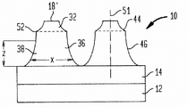
这些过程生成的微触点38如图21A至图21D所示。这些图还示出了应用本文描述的过程可获得的各种外形。参照图21A至图21C,微触点38具有也被称为顶部区域的第一部分32,及也被称为底部区域的第二部分36。倘若在上文所述的步骤中应用的第一光致抗蚀剂片为圆形的,每个微触点将总体上以绕中心轴51(图21A)的旋转体的形式从基板的剩余部分向上以竖直方向或Z向延伸,且总体上垂直于蚀刻停止层14的所在平面。第一部分和第二部分的宽度或直径X在每个部分内沿Z向或高度方向的位置而变化。换言之,在第一部分内,X=F1(Z),且在第二部分内,X=F2(Z)。在第一和第二部分之间的边界52处,斜度或dX/dZ可急剧变化。在每个部分内,斜度或dX/dZ通常沿Z向的位置不急剧变化,因此,不会产生阶跃变化。在每个部分内,典型地沿Z向的位置,斜度或dX/dZ变化是逐步变化的。
进一步如图21A所示,微触点区域的第一部分32的外周面44及第二部分38的外周面46是凹的表面,且每个外周面都具有沿Z向位置逐渐变化的斜度或dX/dZ。关于本文所描述的微触点的每个外周面(例如表面44或表面46(图21A)),“凹陷”是指在外周面的边界之间的每个高度(如,在外周面44的上边界19与外周面44的下边界52之间的每个高度29(图21E)),外周面围起的直径25,小于在相同高度29下,由理论圆锥面围起的直径,理论圆锥面由在边界之间延伸的一系列直线确定。例如,外周面44上在边界19、52之间的每个点,都位于穿过边界19、52延伸的一系列直线确定的理论圆锥面48的内部。
微触点的特定函数及其因此而具有的外形,由在第一蚀刻步骤和第二蚀刻步骤中应用的蚀刻条件而确定。例如,蚀刻剂的成分及蚀刻温度可改变,以改变蚀刻剂浸蚀金属层的速度。蚀刻剂与金属层的接触手段也可改变。蚀刻剂可向基板强制喷洒、或基板可浸入蚀刻剂内。在第一部分和第二部分蚀刻期间,蚀刻条件可为相同的或不同的。
在图21A所示的微触点中,每个第一部分32的外周面44和第二部分36的外周面46都是凹的。另外,在图21A的实施例中,第一部分32具有的外周面44,以朝下的方向向外张开,从而斜度或dX/dZ的量值以朝下的方向增加。第二部分36也具有向外张开的外周面46;在边界52处,第二部分的斜度或dX/dZ的量值为最小值,且沿朝着突柱基底的方向逐渐增加。在边界52处斜度具有实质上改变。在微触点与层14接合的基底,第二部分具有最大宽度或直径X,第二部分的最大宽度或直径X实质上大于第一部分最大宽度或直径。
在图21A至图21D中所看到的每个实施例中,每个微触点的每个部分的外周面都是凹的。这些实施例以其他方式变化。例如,在图21B中,第二部分36的最大宽度仅比第一部分32的最大宽度稍稍大一点。并且,在突柱的基底及边界52之间的某一位置,第二部分具有最小宽度,从而沿向上的方向宽度逐渐减小至最小,然后从最小再沿向上的方向逐渐增加至边界52。这种形状通常称为“冷却塔”形状。在图21B的微触点中,斜度或dX/dZ在两部分之间的边界52处改变符号(sign)。在图21C中,第二部分36在微触点基底附近具有其最小宽度。
最后,图21D示出了具有两个以上部分的微触点的外形。这种类型的外形可由本文描述的过程中的几个步骤进行了数次的情况而导致。因此,可以看出这种特定的微触点38具有四个部分,分别为第一部分32、第二部分36、第三部分40和第四部分42。这四个部分可具有任意的尺寸,且当需要时可比另一部分更宽或更窄。在这个实例中,可具有超过一个的边界。图21A至21D中只是代表性的外形,各种外形都可获得。第一部分32也可称为顶部区域,第四部分42也可称为底部区域,第二部分36和第三部分40可称为中间区域。
尽管在图21A至图21D的每个中仅描述了包括两个微触点或突柱的排列,实际上,可形成包括许多个突柱的突柱阵列。在图21A至21D中描述的每个实施例中,排列中所有微触点或突柱由单一的金属层16(图27)制成。在微触点的基底,每个微触点覆盖蚀刻停止层14的一部分,且微触点与金属层12连接。如将下文所述,在微触点之间的区域通常去除蚀刻停止层14,且通常金属层12被蚀刻或其他方式处理以将其转换为与微触点连接的迹线或其他导电特征。但是,在每个微触点的主体上,从其基底至其顶端是单一体,没有接点如焊点,且通体具有基本均匀的成分。并且,因为在远离层12和14的微触点的端部,微触点的顶端表面18’为金属层16(图14)的初始顶面18的一部分,这些顶端表面基本平坦且水平,且所有微触点的顶端表面基本与其他微触点的顶端表面共面。
在替代实施例中,在第一蚀刻步骤后,不是只在选定的位置去除第一光致抗蚀剂20,全部的第一光致抗蚀剂20可都去除。在这种情况下,第二光致抗蚀剂34可在基板10的整个表面沉积。然后在第二光致抗蚀剂34上放置掩模22。掩模22必须准确对齐,使得仅在先前曝光的位置,在第一微触点部分32上曝光。然后冲洗第二光致抗蚀剂34,并可在基板10进行进一步的蚀刻。
图22是描述第一实施例的流程图。以步骤1100开始,提供基板。然后在步骤1102时,在基板上沉积光致抗蚀剂n。然后在步骤1104时,在光致抗蚀剂n顶上放置掩模。在步骤1106时,在辐射下曝光光致抗蚀剂n。随后,在步骤1108时,除去掩模,然后在步骤1110时,在选定的位置冲洗光致抗蚀剂n及蚀刻基板。
接下来,在步骤1112时沉积被称为n+1的另一光致抗蚀剂。然后,在步骤1114时,这种光致抗蚀剂n+1在辐射下曝光。随后,在步骤1116时,在选定位置上除去光致抗蚀剂n+1,再次蚀刻基板。然后,在步骤1118时判断是否已达到所需的微触点高度。如果没有获得所需的微触点高度,则在步骤1120时,过程返回至步骤1112,在基板上沉积另一光致抗蚀剂。如果在步骤1122时获得了所需的高度,然后在步骤1124除去残留的光致抗蚀剂,过程完成。
图23是描述第二实施例的流程图。第二实施例的步骤1200至1210复制第一实施例中的步骤1100至1110。但是,在步骤1212时,除去全部的光致抗蚀剂n。然后,在步骤1214时,在基板上沉积另一层光致抗蚀剂n+1。接下来,在步骤1216时掩模放回基板上。在这个步骤中,掩模必须对齐,使得其图案基本放置在与掩模在光致抗蚀剂n上放置时的相同位置。随后,在步骤1218时,在辐射下曝光光致抗蚀剂n+1,然后除去掩模。
接下来,在步骤1220时,选择性地去除光致抗蚀剂n+1,并再次蚀刻基板。这个过程也可重复,直到获得所需的微触点高度。因此,在步骤1222时,判断是否达到所需的微触点高度。如果在步骤1224时没有达到优选的高度,则该过程回到步骤1212,光致抗蚀剂已完全除去,并沉积另一光致抗蚀剂n+1,步骤就此继续。但是,如果在步骤1224时已达到所需的高度,在步骤1228时除去剩余的光致抗蚀剂,该过程结束。
蚀刻停止层14和薄层12可用一介电层粘合,然后薄层12可被蚀刻以形成迹线,从而提供了,具有与迹线连接的微触点及从介电层突出的微触点的部件。这样的结构可应用于,例如,作为半导体芯片封装的一个元件。例如,可在美国专利申请号为11/318822,申请日为2005年12月27日的美国专利申请中应用,其公开的内容援引加入本文。
本文描述的结构可为多层基板10整体的一部分,例如,如图24所示,多层基板10的顶层。微触点38可与裸片54焊接。焊料56可浸润(wick)微触点38的一部分。浸润(wicking)提供了微触点38与裸片54之间的良好接触。除了焊料56外,也可应用其他结合工艺。围绕微触点38的是底充胶58,用于把裸片54粘接在微触点38和基板10上。只要需要,任意类型的底充胶58都可应用,或可省去底充胶58。微触点38下方是迹线60及介电层62。端子64位于基板10的底部。
特定的封装包括堆叠的微电子芯片。这使封装在基板上所占据的表面积,小于堆叠中芯片的总表面积。包含应用本文描述的过程制造的微触点的封装可堆叠。可参考同时待审的美国专利申请号为11/140312、申请日为2005年5月27日的美国专利申请;及美国专利号为6782610的美国专利,其公开的内容援引加入本文。这些公开文本中所教导的微触点的蚀刻步骤可用本文描述的过程来替代。
尽管上文描述的为三层金属基板,然而具有任意数量层的适当的基板都可利用,例如,单一金属板。此外,不采用光致抗蚀剂,可采用耐蚀材料如金,或在蚀刻厚金属层时基本抵抗所用的蚀刻剂腐蚀的其他金属。例如,可采用耐蚀金属代替上述的第一光致抗蚀剂20。应用如光致抗蚀剂的掩模后,掩模在所需位置具有容纳耐蚀金属片的孔洞,耐蚀金属片可电镀在厚层16的顶上。在厚层顶部上电镀耐蚀金属后,可蚀刻厚层以形成上文所述的微触点。耐蚀金属可留在微触点的顶端。在耐蚀金属作为第二耐蚀材料(代替上述的第二光致抗蚀剂34)应用的情况下,可用掩模限制第二耐蚀金属的沉积,使之只沉积在微触点的第一部分32上,从而微触点之间的区域保持没有耐蚀金属。替代地,在蚀刻第一微触点部分32后,可除去全部的第一层耐蚀金属,然后可沉积第二层耐蚀金属以保护第一微触点部分32。
参照图25,示出了具有微触点72的微电子单元70。微触点72具有蚀刻停止层74。微触点72从金属层竖直突出,金属层已变成迹线76。在迹线76之间可具有间隙或空间78。第一介电层80可邻近迹线76粘附在单元70的底侧。第一介电层80上的开口82允许迹线76成为电触点。第二介电层84可形成在单元70的顶侧。
由这些过程形成的微触点,可具有的典型高度范围为从约40微米至约200微米。进一步地,微触点之间的典型间距可小于200微米,优选地小于150微米。特别地,参照图26,示出的两个微触点具有顶端直径d和微触点高度h。间距P由两个微触点的纵轴之间的距离确定。
在很多应用中,特别是当微触点应用于与半导体芯片的触点连接时,例如,在参照图27将在下文描述的结构中,提供小的间距是理想的。但是,在微触点从单一金属层上通过单次蚀刻过程而形成的工艺中,通常使间距P小于特定最小间距P0是不实际的。P0与直径d加上高度h的和相等,即,P0=d+h。理论上,最小间距可通过减小顶端直径d而减小。但是,使顶端直径小于零是不可能的。另外,在许多情况下使顶端直径减小至约20或30微米以下是不适当的。例如,触点顶端与用于在蚀刻过程中保护顶端的光致抗蚀剂片之间的粘附力,是与顶端的面积成比例的,因此与顶端直径的平方成比例。因此,在顶端直径很小的情况下,光致抗蚀剂片在过程中会移出原位置。因而,应用传统的工艺,难以形成具有很小间距的微触点。
但是,应用本文描述的过程,微触点的间距可小于P0,(P<P0),例如,P=(0.9)P0或更小。例如,如果顶端的直径d为30微米,高度h为60微米,常规过程将获得为90微米的最小间距P0。但是,在本文描述的过程中,应用至少两次蚀刻过程,可获得的间距P约为80微米或更小。换言之,多级蚀刻过程允许,从单一金属层上形成的单一金属微触点或突柱,具有在常规蚀刻过程中不可达到的间距、顶端直径和高度的组合。随着蚀刻级数的增加,给定顶端直径和高度可获得的最小间距减小。
现在参照图27,示出了微电子封装90,其应用了具有上述的微触点38的封装元件或芯片载体。芯片载体包括第一介电层62,其可由聚酰亚胺、BT树脂或其他通常用于制造芯片载体的介电材料制成。芯片载体还包括与一些或所有微触点38连接的迹线60。迹线与端子61合并。如图27所示,微触点38从介电层62的第一侧,面向上突出。介电层62具有开口82,端子61暴露在第二侧,或通过开口82向下面对第一介电层62的表面暴露。载体进一步包括可选用的第二介电层84。
微触点38的顶端与微电子元件的触点55结合,微电子元件如半导体芯片或裸片54。例如,微触点的顶端可与微电子元件的触点55焊合。也可应用其他的结合工艺,如共熔键合或扩散结合。所得的封装微电子元件,其微电子元件上的一些或全部触点55,通过微触点和迹线,与端子61连接。封装的微电子元件可通过端子61与电路板92上的垫94的结合,而安装至电路板92,如印刷电路板上。例如,在开口82应用焊料球96,电路板92上的垫94可与端子61焊接。
即使在触点紧密排列时,微触点38和微电子元件的触点55之间的连接仍可提供可靠的连接。如上所述,微触点38可形成为具有明显的顶端直径和高度。适当的顶端直径可提供在每个微触点与微电子元件的触点之间提供充足的结合区域。在使用中,芯片54相对于电路板92的热膨胀及收缩的差异,可用微触点38的弯曲及倾斜来调节。这种作用随微触点高度的增加而加强。另外,因为微触点通过共同的金属层形成,在很精密的公差范围内,微触点的高度是均一的。这样方便了微触点顶端与芯片或其他微电子元件的触点之间的接合,及牢固结合的形成。
芯片载体的结构是可改变的。例如芯片载体可只包括一层介电层。迹线可位于介电层的任一侧。替代地,芯片载体可包括多层介电层,且可包括多层迹线,及其他特征,如导电接地面。
本发明进一步的实施例的过程应用具有突柱部分1550的结构(图28),突柱1550从表面1526,如介电层1510的表面突出。突柱部分1550可通过任意过程形成,但优选地以与上文所述类似的蚀刻过程而形成。在突柱部分1550形成后,在突柱部分1550的顶端1533上施加金属或其他导电层1502。例如,层1502可层压在合并有突柱部分1550的结构上,并与突柱部分1550的顶端冶金结合(metallurgically bonded)。可选择性地处理层1502,使得除去远离突柱部分1550的层上的材料,但至少留下覆盖突柱部分1550的部分厚度的层,从而形成与突柱部分1550对齐的附加突柱部分1504(图29),因此形成复合的微触点,每个包括一个靠近基板的基部柱部分1550及远离基板的末梢柱部分1504,末梢柱部分沿竖直方向或Z向从基部柱部分突出。对层1502的处理可包括如上文所述的蚀刻过程,应用与突柱部分1550对齐的耐蚀材料片1506。在蚀刻层1502前,可应用保护层如介电密封剂1508以覆盖突柱部分1550。替代地或附加地,在蚀刻层1502前,突柱部分1550可用电镀或其他方法覆盖耐蚀的导电材料,如镍或金。
构建后续突柱部分的过程可重复,以使在附加突柱部分1504上形成附加部分,从而微触点基本可形成为任意长度。长的微触点使灵活性提高,且突柱顶端的移动量增加。一层或多层介电密封剂可留在环绕已形成的突柱部分的位置,如图28和图29中的层1508,密封剂优选地为柔软的,从而其基本不限制突柱的弯曲。在其他实施例中,密封剂可在部件使用前去除。尽管微触点与类似于上文所述的介电基板1522及迹线1528结合而进行说明,这个过程可用于基本上在任意的结构上制造微触点。
如图29所示,每个微触点具有沿基部柱部分1550的竖直方向或Z向范围而变化的水平或宽度尺寸X,且在基部柱部分1550和末梢柱部分1504之间的接点,微触点的水平或宽度尺寸X以大致为阶跃的方式急剧增加,并且在末梢柱部分的竖直范围内,微触点的水平或宽度尺寸X沿竖直方向变化。在突柱各部分之间的接点,宽度对竖直位置的斜度的变化也是急剧改变的。在每个柱部分内,水平或宽度尺寸变化的模式,根据用于蚀刻或其他形成这种突柱部分的过程而定。例如,在进一步的实施例中,末梢柱部分1504可由如上文所述的多阶段蚀刻过程而形成,从而每个末梢柱部分包括不同的子部分,不同的子部分具有不同的确定宽度X沿竖直方向或Z向变化的函数。
还参照下面的文献,并援引加入本文:美国专利申请:申请号为10/985126,申请日为2004年11月10日;申请号为11/318822,申请日为2005年12月27日;申请号为11/318164,申请日为2005年12月23日;申请号为11/166982,申请日为2005年6月24日;申请号为11/140312,申请日为2005年5月27日;及专利号为7176043的美国专利。
用于形成本文所应用的突柱的过程,可如申请号为11/717,587的美国专利申请中所描述,其公开的内容援引加入本文。
现在参照图30,其示出了封装的微电子组件900的剖视图,封装的微电子组件900为参照图1A至图2A所示并在上文描述的组件的变例,其中从微电子元件902的正面延伸的突柱916,包括多重蚀刻的导电突柱。
如图所示,在这个变例中,封装的微电子组件900包括基板901,基板如图1A所示及上文参照图1A所述。该组件还包括,在面向下或倒装芯片位置的微电子元件902,及使基板与微电子元件接合的导电支柱903。导电支柱903包括在基板901的主表面906上突出的导电凸点或突柱912,且导电凸点或突柱912与从微电子元件902的正面909突出的导电凸点或突柱916对齐。
微电子元件902具有正面909。微电子元件902优选地为半导体芯片或类似物。例如,微电子元件可为裸片。突柱916可从暴露在微电子元件902的正面909的结合垫908上延伸。
如图30所示,导电支柱903包括导电地互连导电突柱912和916的焊料,从而构建了从微电子元件902延伸至基板901的导电支柱903。导电支柱903可通过参照本文其他实施例而公开的任意过程、材料或材料的组合而结合。例如,导电支柱903可在突柱及覆盖材料之间通过共熔键合或阳极键合而结合在一起。
突柱912可为任意类型的导电突柱,包括参照本文其他实施例而公开的导电突柱。例如,突柱912可具有任意的外形,包括截头圆锥。每个导电突柱912的基底和顶端可大致都为圆形或具有不同的形状,例如,长方形或椭圆形。
更具体地,从基板901延伸的突柱912可为如图1A、图1C、图2和图2A所示的突柱108,从而从微电子元件902延伸的突柱916可取代相对应的突柱110,每个突柱都可包括焊料帽130。
在突柱912与突柱916接合之前,突柱912可为图5中所示的突柱208,且每个都包括焊料帽230,从而突柱916可取代相对应的突柱210。突柱912可为图6中所示的突柱308,且每个都包括焊料帽330,从而突柱916可取代相对应的突柱310,每个突柱也都可包括焊料帽330。
在特定的实施例中,突柱912可为图8中所示的突柱508,从而突柱916可取代相对应的突柱510。在这样的实施例中,突柱912和916优选地由弹性或回弹极小的可延展的材料制成,如基本为纯的金,每个突柱设置都为可变形的,以与相对应的突柱接合,而无需应用焊料。
突柱912可为图9至图11中所示的突柱608,从而突柱916可取代相对应的突柱610。在这样的实施例中,突柱912和916优选地包含铜,每个突柱设置为可与相对应的突柱直接熔合,而导电突柱之间无需低熔点金属如焊料或锡存在。
突柱912可为图12中所示的多层基板702的突柱708,从而突柱916可取代相对应的突柱710。在这样的实施例中,突柱912可与从微电子元件902延伸的突柱916直接接合,如通过对突柱顶端进行处理形成的例如金等金属与导电垫和突柱内存在的其他金属之间扩散结合。替代地,突柱912和916可通过易熔金属如焊料、锡或共晶组合物而接合在一起,易熔金属润湿突柱及垫,以形成润湿或焊合的接点。
突柱912可为图13所示的从基板806、806’延伸的突柱812及其他突柱,从而突柱916可取代相应的突柱810、810’。在这样的实施例中,突柱912和916可在堆叠封装组件中应用,堆叠封装组件如图13中所示的组件800、800’。
突柱912和916也可与多层基板一起应用,多层基板如图24中所示的多层基板10。突柱912可为图24中所示的微触点38,突柱916可从微电子元件或其他部件如裸片54上延伸,从而突柱912可应用焊料,或本文描述的其他突柱结合工艺,而与突柱916结合。
突柱912可为图25中所示的微触点72,突柱912从金属层上竖直突出,金属层已变成迹线76。
突柱912可为图27中所示的微触点38,突柱912从包括迹线60、开口82、端子61及可选用的第二介电层84的基板延伸。
突柱916为多重蚀刻的导电突柱。如图30所示,突柱916与图21B中所示的双重蚀刻的微触点38相同。如上文参照图21B所描述的,每个突柱916总体上为绕沿竖直方向或Z向延伸的中心轴的旋转体形式,从微电子元件902向下,且基本垂直于正面909所在平面而延伸。
在其他实施例中(未示出),突柱916可为任意多重蚀刻的导电突柱,包括例如,图21A、图21C和图21D所示的多重蚀刻的微触点38。尽管在图30中所示的突柱916是被双重蚀刻的,突柱916可进行超过两次的蚀刻,如图21D中所示的四次蚀刻。
突柱916可为具有图28和图29中所示结构的复合微触点,其中每个突柱916包括邻近微电子元件902的基部柱部分1550,及远离微电子元件的末梢柱部分1504。
现在参照图31,其示出了封装的微电子组件920的剖视图,封装的微电子组件920为图1A至图2A中所示及上文参照图1A至图2A所描述的组件的变例,其中从基板921的顶面延伸的突柱932,包括多重蚀刻的导电突柱。
图31所示的封装的微电子组件920基本与图30所示的封装微电子组件900相同,除了从基板921上延伸的突柱932为多重蚀刻突柱以外,突柱932如图21B所示的双重蚀刻的微触点38,而从微电子元件922延伸的突柱936可为任意类型的导电突柱,包括参照本文其他实施例而公开的任意类型的导电突柱。
如图所示,在这个变例中,封装微电子组件920包括如图1A所示及在上文参照图1A所描述的基板921。该组件还包括在面向下或倒装芯片位置的微电子元件922,及使基板与微电子元件接合的导电支柱923。导电支柱923包括在基板921主表面926上突出的导电凸点或突柱932,导电凸点或突柱932与在微电子元件922的正面929上突出的导电凸点或突柱936对齐。
如图31所示,导电支柱923包括导电地互连导电突柱932和936的焊料,从而构建了从微电子元件922延伸至基板921的导电支柱923。导电支柱923可通过参照本文其他实施例而公开的任意过程、材料或材料的组合而结合在一起。
突柱932是多重蚀刻的导电突柱。如图31所示,突柱932与图21B中所示的双重蚀刻的微触点38相同。在其他实施例中(未示出),突柱932可为任意多重蚀刻的导电突柱,包括例如,图21A、21C及图21D所示的多重蚀刻的微触点38。尽管在图31中所示的突柱32是双重蚀刻的,突柱932可进行超过两次的蚀刻,如图21D所示的四次蚀刻。突柱932可为具有图28和图29所示结构的复合微触点,其中每个突柱932包括邻近基板922的基部柱部分1550及远离基板的末梢柱部分1504。
突柱936可为任意类型的导电突柱,包括参照本文其他实施例而公开的任意类型的导电突柱。例如,突柱936可具有任意外形,包括截头圆锥形。每个导电突柱936的基底和顶端可都基本为圆形的,或具有不同形状,如长方形或椭圆形。
更具体地,从微电子元件922延伸的突柱936可为图1B、图2和图2A中所示的突柱110,从而从基板921延伸的突柱932可取代相对应的突柱108。突柱936中每个都可包括焊料帽130。
在突柱936与突柱932接合之前,突柱936可为图5中所示的突柱210,从而突柱932可取代相对应的包括焊料帽230的突柱208。突柱936可为图6中所示的突柱310,每个都包括焊料帽330,从而突柱932可取代相对应的突柱308,每个突柱也都包括焊料帽330。
在特定实施例中,突柱936可为图8中所示的突柱510,从而突柱932可取代相对应的突柱508。在这样的实施例中,突柱932和936优选地由弹性或回弹极小的可延展材料制成,如基本为纯的金,每个突柱设置为可变形的,以与相对应的突柱接合,而无需应用焊料。
突柱936可为图9至图11所示的突柱610,从而突柱932可取代相对应的突柱608。在这样的实施例中,突柱932和936优选地由铜制成,且每个突柱设置为与相对应的突柱直接熔合,而在导电突柱之间无需低熔点金属,如焊料或锡的存在。
突柱936可为图13所示的突柱810、810’,从而突柱932可取代从基板806、806’上延伸的相对应的突柱。在这样的实施例中,突柱932和936可应用于如图13所示组件800、800’的堆叠封装组件。
突柱932和936可与多层基板一起应用,多层基板如图24所示的多层基板10。突柱932可为图24中所示的微触点38,突柱936可从微电子元件或其他部件如裸片54上延伸,从而突柱932可应用焊料,或本文描述的其他突柱结合工艺,而与突柱936结合。
现在参照图32,其示出了堆叠微电子组件940的剖视图,堆叠微电子组件940为图1A至图2A所示及上文参照图1A至图2A所描述的组件的变例,其中突柱952从基板941的顶面延伸,从微电子元件941的正面延伸的突柱956,包括多重蚀刻的导电突柱。
图32中所示的封装微电子组件940基本与图30中所示的封装微电子组件900及图31中所示的封装微电子组件920相同,除了从基板941上延伸的突柱952和从微电子元件942上延伸的突柱956都是多重蚀刻的导电突柱以外,突柱如图21B所示的双重蚀刻的微触点38。
如图所示,在这个变例中,封装的微电子组件940包括如图1A所示及上文参照图1A所述的基板941。组件还包括在面向下或倒状芯片位置的微电子元件942,及使基板与微电子元件接合的导电支柱943。导电支柱943包括在基板941的主表面946上突出的凸点或突柱952,凸点或突柱952与从微电子元件942的正面949上突出的凸点或突柱956对齐。
如图32所示,导电支柱943包括与导电突柱952和956导电互连的焊料,从而构建了从微电子元件942延伸至基板941的导电支柱943。导电支柱943可通过参照本文其他实施例而公开的任意过程、材料或材料的组合而结合在一起。
突柱952和956是多重蚀刻的导电突柱。如图32所示,突柱952和956都与图21B中所示双重蚀刻的微触点38相同。在其他实施例中(未示出),突柱952和956可为任意多重蚀刻的导电突柱,包括例如,图21A、21C和图21D中所示的多重蚀刻的微触点38。
尽管所示的突柱952和956都与图21B中所示的双重蚀刻的微触点38相同,在其他实施例中(未示出),突柱952可具有与突柱956不同的多重蚀刻形状,包括,例如,突柱952可为如图21A所示形状,突柱956可为图21C所示的形状,确定突柱952外形的第一函数和第二函数由在突柱952的第一蚀刻和第二蚀刻步骤中应用的蚀刻条件确定,确定突柱956外形的第三函数和第四函数由在突柱956的第一蚀刻和第二蚀刻步骤中所应用的蚀刻条件而确定,第一函数和第二函数可与第三函数和第四函数不同。
尽管图32中所示突柱952和956是双重蚀刻的,突柱952和956中的任一或两者都可进行超过两次的蚀刻,如图21D中所示的四次蚀刻。突柱952和956可为具有图28和29所示结构的复合微触点,其中每个突柱952和956都包括,邻近基板942的基部柱部分1550及远离基板的末梢柱部分1504。
更具体地,突柱952和956中任一或两者都可包括焊料帽,如图1B、图1C、图5和图6所示。
与图8中所示实施例类似,突柱952和956可由弹性或回弹极小的可延展材料制成,例如,基本纯的金,每个突柱设置为可变形的,以与相对应的突柱接合,而无需应用焊料。
与图9中所示的实施例类似,突柱952和956可包含铜,每个突柱可设置为可直接与相对应的突柱熔合,而在导电突柱之间无需低熔点金属如焊料或锡存在。
突柱952和956可在如图13所示组件800、800’的堆叠封装组件中应用。突柱952和956可与多层基板一起应用,多层基板如图24所示的多层基板10。
现在参照图33,其示出了堆叠微电子组件960的剖视图,堆叠微电子组件960为图1A至图2A所示及上文参照图1A至图2A所描述的组件的变例,其中从基板961顶面延伸的突柱972,包括多重蚀刻的导电突柱。
图33中所示的封装微电子组件960,基本与图31中所示的封装微电子组件920相同,除了从微电子元件962延伸的突柱976具有截头圆锥形状以外,如参照本文其他实施例而公开的任意截头圆锥突柱或微触点。
如图所示,在这个变例中,封装微电子组件960包括如图1A所示及上文参照图1A所描述的基板961。该组件也可包括在面向下或倒装芯片位置的微电子元件962,及使基板与微电子元件接合的导电支柱963。导电支柱963包括在基板961的主表面966上突出的导电凸点或突柱972,导电凸点或突柱972与在微电子元件962正面969上突出的导电凸点或突柱976对齐。
如图33所示,导电支柱963包括导电地互连导电突柱972和976的焊料,从而构建了从微电子元件962延伸至基板961的导电支柱963。导电支柱963可通过参照本文其他实施例而公开的任意过程、材料或材料的组合而结合在一起。
突柱972为多重蚀刻的导电突柱。如图33所示,突柱972与图21B中所示双重蚀刻的微触点38相同。在其他实施例中(未示出),突柱972可为任意多重蚀刻导电突柱,包括例如图21A、图21C和图21D中所示的多重蚀刻微触点。尽管在图33中所示的突柱972是经双重蚀刻的,突柱972可进行超过两次的蚀刻过程,如图21D所示的四次蚀刻。突柱972可为具有图28和图29所示结构的复合微触点,其中每个突柱972包括邻近基板962的基部柱部分1550和远离基板的末梢柱部分1504。
更具体地,突柱972和976中任一或二者都可包括焊料帽,如图1B、图1C、图5和图6所示。
与图8所示的实施例类似,突柱972和976可由弹性或回弹极小的可延展材料制成,例如,基本为纯的金,且每个突柱都设置为可变形的,以与相对应的突柱接合,而无需应用焊料。
与图9中所示的实施例类似,突柱972和976可包含铜,每个突柱都可设置为直接与相对应的突柱直接熔合在一起,而在导电突柱之间无需低熔点金属如焊料或锡存在。
突柱972和976可在如图13所示组件800、800’的堆叠封装组件中应用。突柱972和976可与多层基板一起应用,多层基板如图24所示的多层基板10。
现在参照图34,其示出了封装的微电子组件980的剖视图,封装的微电子组件980为图1A至图2A所示及上文参照图1A至图2A所描述的组件的变例,其中从微电子元件982的正面延伸的突柱996包括多重蚀刻的导电突柱。
图33中所示的封装的微电子组件980,基本与图30中所示的封装的微电子组件900类似,除了图30中从基板901延伸的突柱912,被粘附至基板981的结合垫992取代以外,结合垫992可如参照本文其他实施例而公开的任意结合垫。
如图所示,在这个变例中,封装的微电子组件980包括如图1A所示及上文参照图1A所描述的基板981。该组件还包括在面向下或倒装芯片位置的微电子元件982,及使基板与微电子元件接合的导电支柱983。导电突柱983包括附接至基板981主表面986的导电结合垫992,导电结合垫992与从微电子元件982的正面989上突出的导电凸点或突柱996对齐。
如图34所示,导电支柱983包括导电地互连导电突柱996和垫992的焊料,从而构建了从微电子元件982延伸至基板981的导电支柱983。导电支柱983可通过参照本文其他实施例而公开的任意过程、材料、或材料的组合而结合在一起。
突柱996为多重蚀刻导电突柱。如图34所示,突柱996与图21B中所示的双重蚀刻的微触点38相同。在其他实施例中(未示出),突柱996可为任意多次蚀刻的导电突柱,包括例如图21A、图21C和图21D中所示的多重蚀刻微触点。尽管图33中所示突柱996为双重蚀刻的,突柱996可进行超过两次的蚀刻,如图21D中所示四次蚀刻。突柱996可为具有图28和图29所示结构的复合微触点,其中每个突柱996都包括邻近微电子元件981的基部柱部分1550及远离微电子元件的末梢柱部分1504。
更具体地,垫992和突柱996中任一个或两者都可包括焊料帽,如图1B、图1C、图5和图6所示。
与图8所示的实施例类似,垫992和突柱996由弹性或回弹极小的可延展材料制成,例如,基本纯的金,每个突柱设置为可变形的,以与相对应的突柱接合,而无需应用焊料。
与图9所示实施例类似,垫992和突柱996可包括铜,每个突柱可设置为可直接与相对应突柱熔合,而在导电突柱之间无需低熔点金属如焊料或锡存在。
垫992和突柱996可在如图13所示组件800、800’的堆叠封装组件中应用。垫992和突柱996可与多层基板一起应用,多层基板如图24所示多层基板10。
现在参照图35,其示出了封装的微电子组件1000的剖视图,封装的微电子组件1000为图1A至图2A所示及上文参照图1A至图2A所描述的组件的变例,其中突柱1012从基板1001顶面延伸,从微电子元件1002的正面延伸的突柱1016包括多重蚀刻导电突柱。
图35所示的封装的微电子组件1000与图32所示的封装的微电子组件940相同,除了导电支柱1003内导电互连导电突柱1012和1016的焊料没有与微电子元件1002的导电垫1008接触以外。在特定实施例中,导电支柱1003内的焊料不与基板1001的主表面1006接触,或不与垫(未示出)接触,基板的突柱1012从所述垫上延伸,这种垫可暴露在基板的主表面1006上。
图30至图34中所示的导电支柱903、923、943、963和983设置为,用于为芯片在基板上的封装增加高度,通过增加微电子元件和基板之间的间隔距离或竖直距离,且同时允许导电支柱之间中心至中心水平距离或间距减小。增加基板与微电子元件之间距离的能力可有助于减小导电支柱的应力,可有助于方便底充胶的应用(例如,可参见图2A),及允许应用更多种类的底充胶。
图30中所示的突柱912和916、图31中所示的突柱932和936、图32中所示的突柱952和956、图33中所示的突柱972和976、及图34中所示的结合垫992和突柱996,都可由任意的导电材料制成,如铜、铜合金、金及其组合物。图31中所示的突柱932和936、图32中所示的突柱952和956、图33中所示的突柱972和976、及图34中所示的结合垫992和突柱996,都可包括可被焊料润湿的暴露的金属层。例如,各突柱可包含铜,且突柱表面具有金层。此外,图31中所示的突柱932和936、图32中所示的突柱952和956、图33中所示的突柱972和976、及图34中所示的结合垫992和突柱996,都可包括至少一层熔点高于待接合焊料熔点的金属。例如,这种导电突柱可包括铜层或全部由铜制成。
图31中所示的突柱932和936、图32中所示的突柱952和956、图33中所示的突柱972和976、及图34中所示突柱996的尺寸都可在显著的范围内变化,但最典型地,从基板及微电子元件的正面延伸的突柱中每个的高度为至少30微米,且可延伸高达300微米。这些突柱的高度(分别大致垂直于基板及微电子元件的正面)可比其直径或宽度(分别大致与基板及微电子元件的正面平行)更大。但是,该高度也可比宽度小,如为宽度大小的至少一半。
用于使例如半导体芯片这样的微电子元件与例如芯片载体这样的基板电连接的过程,可如申请号为12/286102的美国专利申请中进一步所描述,其援引加入本文。
尽管本发明参照特定实施例进行描述,可以理解的是,这些实施例只是说明本发明的原则和应用。因此,应理解为,在不偏离由附加的权利要求书所确定的本发明精神和范围的情况下,说明的实施例可做出许多修改及可设计出其他布置。
可是理解的是,各从属权利要求及其设定的特征可以与存在于最初权利要求书中的不同的方式组合。也可理解的是,与单个实施例结合进行描述的特征可与其他已描述的实施例共享。
Claims (47)
1. 封装的微电子元件,包括:
微电子元件,具有正面和从所述正面向外延伸的复数个实心金属突柱;及
基板,具有主表面和暴露在所述主表面的复数个导电元件,所述导电元件与所述实心金属突柱接合;
每个实心金属突柱包括邻近所述微电子元件的底部区域及远离所述微电子元件的顶部区域,所述底部区域与所述顶部区域分别具有凹的外周面;
每个实心金属突柱具有一水平尺寸,在所述底部区域内所述水平尺寸为竖直位置的第一函数,在所述顶部区域内所述水平尺寸为竖直位置的第二函数。
2. 根据权利要求1所述的封装的微电子元件,其中每个实心金属突柱进一步包括至少一个位于所述底部区域和所述顶部区域之间的中间区域,所述中间区域具有凹的外周面,在所述中间区域内,每个实心金属突柱的水平尺寸为竖直位置的第三函数。
3. 根据权利要求1所述的封装的微电子元件,其中每个实心金属突柱具有沿所述正面方向的宽度以及从所述正面延伸的高度,其中所述高度至少为所述宽度的一半。
4. 根据权利要求1所述的封装的微电子元件,其中所述实心金属突柱与所述导电元件采用易熔金属而接合。
5. 根据权利要求4所述的封装的微电子元件,其中所述易熔金属包括焊料,所述焊料覆盖每个实心金属突柱的至少部分的边缘表面。
6. 根据权利要求5所述的封装的微电子元件,进一步包括位于所述正面的复数个导电垫,其中每个实心金属突柱从所述复数个导电垫中相应的一个上延伸,且所述焊料不与所述复数个导电垫中的至少一个接触。
7. 根据权利要求5所述的封装的微电子元件,其中所述焊料不与任一实心金属突柱的底部区域接触。
8. 根据权利要求4所述的封装的微电子元件,其中所述易熔金属包括焊料,且所述焊料只与每个实心金属突柱的顶面接触。
9. 根据权利要求1所述的封装的微电子元件,其中每个实心金属突柱的高度为所述微电子元件的所述正面与所述基板的所述主表面之间距离的25%至50%之间。
10. 根据权利要求1所述的封装的微电子元件,其中每个实心金属突柱的高度为所述微电子元件的所述正面与所述基板的所述主表面之间距离的至少40%。
11. 根据权利要求1所述的封装的微电子元件,其中所述实心金属突柱与所述导电元件扩散结合在一起。
12. 根据权利要求1所述的封装的微电子元件,其中所述第一函数和所述第二函数实质上不同。
13. 根据权利要求1所述的封装的微电子元件,其中在所述实心金属突柱的所述底部区域与所述顶部区域的交界处,水平尺寸相对竖直位置的斜度急剧变化。
14. 根据权利要求1所述的封装的微电子元件,其中所述实心金属突柱和所述导电元件基本上由铜组成。
15. 根据权利要求1所述的封装的微电子元件,其中所述导电元件包括导电垫,所述导电垫与所述实心金属突柱接合。
16. 根据权利要求1所述的封装的微电子元件,其中所述实心金属突柱为第一实心金属突柱,所述导电元件包括复数个第二实心金属突柱,所述第二实心金属突柱在所述主表面上方延伸且与所述第一实心金属突柱接合,所述第二突柱具有远离所述基板的所述主表面的顶面,及以大角度远离所述顶面延伸的边缘表面。
17. 根据权利要求16所述的封装的微电子元件,其中所述第一实心金属突柱与所述第二实心金属突柱采用易熔金属而接合。
18. 根据权利要求17所述的封装的微电子元件,其中所述易熔金属包括焊料,所述焊料覆盖每个实心金属突柱的至少部分的边缘表面。
19. 根据权利要求18所述的封装的微电子元件,进一步包括,位于所述正面的复数个导电垫,其中每个第一实心金属突柱从所述复数个导电垫中相应的一个上延伸,且所述焊料不与所述复数个导电垫中的至少一个接触。
20. 根据权利要求17所述的封装的微电子元件,其中所述易熔金属包括焊料,所述焊料只与每个实心金属突柱的顶面接触。
21. 根据权利要求16所述的封装的微电子元件,其中所述第一实心金属突柱与所述第二实心金属突柱扩散结合在一起。
22. 根据权利要求16所述的封装的微电子元件,其中每个第二实心金属突柱包括邻近所述基板的底部区域以及远离所述基板的顶部区域,每个第二实心金属突柱的所述底部区域和所述顶部区域分别具有凹的外周面,每个第二实心金属突柱具有一水平尺寸,在所述底部区域内所述水平尺寸为竖直位置的第三函数,在所述顶部区域内所述水平尺寸为竖直位置的第四函数。
23. 根据权利要求22所述的封装的微电子元件,其中每个第二实心金属突柱具有沿所述主表面方向的宽度及从所述主表面延伸的高度,其中所述高度至少为所述宽度的一半。
24. 根据权利要求22所述的封装的微电子元件,其中所述第一实心金属突柱与所述第二实心金属突柱采用易熔金属而接合。
25. 根据权利要求24所述的封装的微电子元件,其中所述易熔金属包括焊料,所述焊料覆盖每个实心金属突柱的至少部分的边缘表面。
26. 根据权利要求25所述的封装的微电子元件,进一步包括位于所述正面的复数个导电垫,其中每个第一实心金属突柱从所述复数个导电垫中相应的一个上延伸,且所述焊料不与所述复数个导电垫中的至少一个接触。
27. 根据权利要求25所述的封装的微电子元件,其中所述焊料不与任一实心金属突柱的底部区域接触。
28. 根据权利要求24所述的封装的微电子元件,其中所述易熔金属包括焊料,且所述焊料只与每个实心金属突柱的顶面接触。
29. 根据权利要求22所述的封装的微电子元件,其中所述第一实心金属突柱与所述第二实心金属突柱扩散结合在一起。
30. 根据权利要求22所述的封装的微电子元件,其中所述第一函数与所述第三函数相同,所述第二函数与所述第四函数相同。
31. 封装的微电子元件,包括:
微电子元件,具有正面和在所述正面上突出的复数个第一实心金属突柱,所述第一突柱具有远离所述正面的顶面及以大角度从所述正面向外延伸的边缘表面;及
基板,具有主表面和从所述主表面延伸的复数个第二实心金属突柱,所述第二实心金属突柱与所述第一实心金属突柱接合;
每个第二实心金属突柱包括邻近所述微电子元件的底部区域及远离所述微电子元件的顶部区域,所述底部区域与所述顶部区域分别具有凹的外周面;
每个第二实心金属突柱具有一水平尺寸,在所述底部区域内所述水平尺寸为竖直位置的第一函数,在所述顶部区域内所述水平尺寸为竖直位置的第二函数。
32. 根据权利要求31所述的封装的微电子元件,其中每个第一突柱具有截头圆锥的外形。
33. 根据权利要求31所述的封装的微电子元件,其中每个第二突柱具有沿所述主表面方向的宽度及从所述主表面延伸的高度,其中所述高度至少为所述宽度的一半。
34. 根据权利要求31所述的封装的微电子元件,其中所述第一实心金属突柱与所述第二实心金属突柱采用易熔金属而接合。
35. 根据权利要求34所述的封装的微电子元件,其中所述易熔金属包括焊料,所述焊料覆盖每个实心金属突柱的至少部分的边缘表面。
36. 根据权利要求35所述的封装的微电子元件,进一步包括位于所述正面的复数个导电垫,其中每个第一实心金属突柱从所述复数个导电垫中相应的一个上延伸,且所述焊料不与所述复数个导电垫中的至少一个接触。
37. 根据权利要求34所述的封装的微电子元件,其中所述易熔金属包括焊料,所述焊料只与每个实心金属突柱的顶面接触。
38. 根据权利要求31所述的封装的微电子元件,其中所述第一实心金属突柱与所述第二实心金属突柱扩散结合在一起。
39. 封装的微电子元件的组装方法,包括:
(a)提供微电子元件,所述微电子元件具有正面和在所述正面上以竖直方向突起的复数个实心金属突柱,每个实心金属突柱包括邻近所述正面的底部区域及远离所述正面的顶部区域,所述底部区域与所述顶部区域分别具有凹的外周面,每个实心金属突柱具有一水平尺寸,在所述底部区域内所述水平尺寸为竖直位置的第一函数,在所述顶部区域内所述水平尺寸为竖直位置的第二函数;
(b)使所述复数个实心金属突柱与在基板的主表面上暴露的复数个导电元件至少基本对齐;及
(c)使所述微电子元件的所述实心金属突柱与所述基板的所述导电元件接合。
40. 根据权利要求39所述的方法,其中步骤(c)包括加热易熔金属至熔化温度,其中所述易熔金属流至所述实心金属突柱的边缘表面的暴露部分上。
41. 根据权利要求40所述的方法,其中所述易熔金属包括焊料,所述焊料覆盖每个实心金属突柱的至少部分的边缘表面。
42. 根据权利要求41所述的方法,进一步包括位于所述正面的复数个导电垫,其中每个第一实心金属突柱从所述复数个导电垫中相应的一个上延伸,且所述焊料不与所述复数个导电垫中的至少一个接触。
43. 根据权利要求41所述的方法,其中所述焊料不与任一实心金属突柱的底部区域接触。
44. 根据权利要求40所述的方法,其中所述易熔金属包括焊料,且所述焊料只与每个实心金属突柱的顶面接触。
45. 根据权利要求39所述的方法,其中每个实心金属突柱的高度为所述微电子元件的所述正面与所述基板的所述主表面之间距离的25%至50%之间。
46. 根据权利要求39所述的方法,其中每个实心金属突柱的高度为所述微电子元件的所述正面与所述基板的所述主表面之间距离的至少40%。
47. 根据权利要求39所述的方法,其中钝化层和凸点下金属化层沉积在所述微电子元件上。
Applications Claiming Priority (3)
| Application Number | Priority Date | Filing Date | Title |
|---|---|---|---|
| US12/832,376 US8330272B2 (en) | 2010-07-08 | 2010-07-08 | Microelectronic packages with dual or multiple-etched flip-chip connectors |
| US12/832,376 | 2010-07-08 | ||
| PCT/US2011/043152 WO2012006403A1 (en) | 2010-07-08 | 2011-07-07 | Microelectronic package with dual or multiple - etched flip -chip connectors and corresponding manufacturing method |
Publications (1)
| Publication Number | Publication Date |
|---|---|
| CN103201835A true CN103201835A (zh) | 2013-07-10 |
Family
ID=44513123
Family Applications (1)
| Application Number | Title | Priority Date | Filing Date |
|---|---|---|---|
| CN2011800428536A Pending CN103201835A (zh) | 2010-07-08 | 2011-07-07 | 具有双重或多重蚀刻倒装芯片连接体的微电子封装和相应的制造方法 |
Country Status (7)
| Country | Link |
|---|---|
| US (2) | US8330272B2 (zh) |
| EP (1) | EP2591501A1 (zh) |
| JP (2) | JP2013534060A (zh) |
| KR (1) | KR101865234B1 (zh) |
| CN (1) | CN103201835A (zh) |
| TW (1) | TWI456717B (zh) |
| WO (1) | WO2012006403A1 (zh) |
Cited By (7)
| Publication number | Priority date | Publication date | Assignee | Title |
|---|---|---|---|---|
| CN104217969A (zh) * | 2014-08-28 | 2014-12-17 | 南通富士通微电子股份有限公司 | 半导体器件封装方法 |
| CN105895604A (zh) * | 2015-02-17 | 2016-08-24 | 南茂科技股份有限公司 | 半导体装置 |
| CN106057685A (zh) * | 2016-07-28 | 2016-10-26 | 合肥矽迈微电子科技有限公司 | 封装方法及倒装芯片封装结构 |
| CN106409793A (zh) * | 2015-07-29 | 2017-02-15 | 乾坤科技股份有限公司 | 具有电磁屏蔽结构的电子模组及其制造方法 |
| US10531558B2 (en) | 2015-07-29 | 2020-01-07 | Cyntec Co., Ltd. | Electronic module having electromagnetic shielding structure and manufacturing method thereof |
| CN112117248A (zh) * | 2019-06-20 | 2020-12-22 | 矽品精密工业股份有限公司 | 电子封装件及其制法 |
| CN112466828A (zh) * | 2019-09-06 | 2021-03-09 | 铠侠股份有限公司 | 半导体装置 |
Families Citing this family (86)
| Publication number | Priority date | Publication date | Assignee | Title |
|---|---|---|---|---|
| KR101313391B1 (ko) | 2004-11-03 | 2013-10-01 | 테세라, 인코포레이티드 | 적층형 패키징 |
| US8058101B2 (en) | 2005-12-23 | 2011-11-15 | Tessera, Inc. | Microelectronic packages and methods therefor |
| US8569876B2 (en) | 2006-11-22 | 2013-10-29 | Tessera, Inc. | Packaged semiconductor chips with array |
| US8558379B2 (en) | 2007-09-28 | 2013-10-15 | Tessera, Inc. | Flip chip interconnection with double post |
| WO2009048604A2 (en) | 2007-10-10 | 2009-04-16 | Tessera, Inc. | Robust multi-layer wiring elements and assemblies with embedded microelectronic elements |
| JP2010161136A (ja) * | 2009-01-07 | 2010-07-22 | Panasonic Corp | 半導体装置及びその製造方法 |
| US8330272B2 (en) * | 2010-07-08 | 2012-12-11 | Tessera, Inc. | Microelectronic packages with dual or multiple-etched flip-chip connectors |
| US8482111B2 (en) | 2010-07-19 | 2013-07-09 | Tessera, Inc. | Stackable molded microelectronic packages |
| US9159708B2 (en) | 2010-07-19 | 2015-10-13 | Tessera, Inc. | Stackable molded microelectronic packages with area array unit connectors |
| US9640437B2 (en) | 2010-07-23 | 2017-05-02 | Tessera, Inc. | Methods of forming semiconductor elements using micro-abrasive particle stream |
| US8580607B2 (en) | 2010-07-27 | 2013-11-12 | Tessera, Inc. | Microelectronic packages with nanoparticle joining |
| US8610259B2 (en) | 2010-09-17 | 2013-12-17 | Tessera, Inc. | Multi-function and shielded 3D interconnects |
| US8847380B2 (en) | 2010-09-17 | 2014-09-30 | Tessera, Inc. | Staged via formation from both sides of chip |
| US8736066B2 (en) | 2010-12-02 | 2014-05-27 | Tessera, Inc. | Stacked microelectronic assemby with TSVS formed in stages and carrier above chip |
| US8587126B2 (en) | 2010-12-02 | 2013-11-19 | Tessera, Inc. | Stacked microelectronic assembly with TSVs formed in stages with plural active chips |
| US8610264B2 (en) | 2010-12-08 | 2013-12-17 | Tessera, Inc. | Compliant interconnects in wafers |
| US8502340B2 (en) | 2010-12-09 | 2013-08-06 | Tessera, Inc. | High density three-dimensional integrated capacitors |
| US8742541B2 (en) | 2010-12-09 | 2014-06-03 | Tessera, Inc. | High density three-dimensional integrated capacitors |
| US8853558B2 (en) | 2010-12-10 | 2014-10-07 | Tessera, Inc. | Interconnect structure |
| US20120146206A1 (en) * | 2010-12-13 | 2012-06-14 | Tessera Research Llc | Pin attachment |
| KR101128063B1 (ko) | 2011-05-03 | 2012-04-23 | 테세라, 인코포레이티드 | 캡슐화 층의 표면에 와이어 본드를 구비하는 패키지 적층형 어셈블리 |
| US8618659B2 (en) | 2011-05-03 | 2013-12-31 | Tessera, Inc. | Package-on-package assembly with wire bonds to encapsulation surface |
| US8404520B1 (en) | 2011-10-17 | 2013-03-26 | Invensas Corporation | Package-on-package assembly with wire bond vias |
| US8952529B2 (en) | 2011-11-22 | 2015-02-10 | Stats Chippac, Ltd. | Semiconductor device with conductive layer over substrate with vents to channel bump material and reduce interconnect voids |
| JP2013115214A (ja) * | 2011-11-28 | 2013-06-10 | Shinko Electric Ind Co Ltd | 半導体装置、半導体素子、及び半導体装置の製造方法 |
| US8653658B2 (en) * | 2011-11-30 | 2014-02-18 | Taiwan Semiconductor Manufacturing Company, Ltd. | Planarized bumps for underfill control |
| US9659893B2 (en) | 2011-12-21 | 2017-05-23 | Mediatek Inc. | Semiconductor package |
| US8633588B2 (en) | 2011-12-21 | 2014-01-21 | Mediatek Inc. | Semiconductor package |
| TWI467718B (zh) * | 2011-12-30 | 2015-01-01 | Ind Tech Res Inst | 凸塊結構以及電子封裝接點結構及其製造方法 |
| US8946757B2 (en) | 2012-02-17 | 2015-02-03 | Invensas Corporation | Heat spreading substrate with embedded interconnects |
| US8372741B1 (en) | 2012-02-24 | 2013-02-12 | Invensas Corporation | Method for package-on-package assembly with wire bonds to encapsulation surface |
| US9553040B2 (en) | 2012-03-27 | 2017-01-24 | Mediatek Inc. | Semiconductor package |
| US20130256895A1 (en) * | 2012-03-30 | 2013-10-03 | Michael Su | Stacked semiconductor components with universal interconnect footprint |
| US9299674B2 (en) | 2012-04-18 | 2016-03-29 | Taiwan Semiconductor Manufacturing Company, Ltd. | Bump-on-trace interconnect |
| US8835228B2 (en) | 2012-05-22 | 2014-09-16 | Invensas Corporation | Substrate-less stackable package with wire-bond interconnect |
| US9391008B2 (en) | 2012-07-31 | 2016-07-12 | Invensas Corporation | Reconstituted wafer-level package DRAM |
| US9502390B2 (en) | 2012-08-03 | 2016-11-22 | Invensas Corporation | BVA interposer |
| US9111817B2 (en) * | 2012-09-18 | 2015-08-18 | Taiwan Semiconductor Manufacturing Company, Ltd. | Bump structure and method of forming same |
| CN202816916U (zh) * | 2012-10-10 | 2013-03-20 | 矽力杰半导体技术(杭州)有限公司 | 一种倒装封装装置 |
| US9385098B2 (en) * | 2012-11-21 | 2016-07-05 | Nvidia Corporation | Variable-size solder bump structures for integrated circuit packaging |
| US8878353B2 (en) | 2012-12-20 | 2014-11-04 | Invensas Corporation | Structure for microelectronic packaging with bond elements to encapsulation surface |
| CN103904050B (zh) * | 2012-12-28 | 2017-04-19 | 碁鼎科技秦皇岛有限公司 | 封装基板、封装基板制作方法及封装结构 |
| US9136254B2 (en) | 2013-02-01 | 2015-09-15 | Invensas Corporation | Microelectronic package having wire bond vias and stiffening layer |
| TWI490962B (zh) * | 2013-02-07 | 2015-07-01 | Univ Nat Chiao Tung | 電性連接結構及其製備方法 |
| US9167710B2 (en) | 2013-08-07 | 2015-10-20 | Invensas Corporation | Embedded packaging with preformed vias |
| US9685365B2 (en) | 2013-08-08 | 2017-06-20 | Invensas Corporation | Method of forming a wire bond having a free end |
| US10074581B2 (en) * | 2013-08-30 | 2018-09-11 | Mediatek Inc. | Chip package having a patterned conducting plate and a conducting pad with a recess |
| US20150076714A1 (en) | 2013-09-16 | 2015-03-19 | Invensas Corporation | Microelectronic element with bond elements to encapsulation surface |
| US9583456B2 (en) | 2013-11-22 | 2017-02-28 | Invensas Corporation | Multiple bond via arrays of different wire heights on a same substrate |
| US9379074B2 (en) | 2013-11-22 | 2016-06-28 | Invensas Corporation | Die stacks with one or more bond via arrays of wire bond wires and with one or more arrays of bump interconnects |
| US9263394B2 (en) | 2013-11-22 | 2016-02-16 | Invensas Corporation | Multiple bond via arrays of different wire heights on a same substrate |
| US9508637B2 (en) | 2014-01-06 | 2016-11-29 | Taiwan Semiconductor Manufacturing Company, Ltd. | Protrusion bump pads for bond-on-trace processing |
| US9275967B2 (en) | 2014-01-06 | 2016-03-01 | Taiwan Semiconductor Manufacturing Company, Ltd. | Protrusion bump pads for bond-on-trace processing |
| US9418928B2 (en) | 2014-01-06 | 2016-08-16 | Taiwan Semiconductor Manufacturing Company, Ltd. | Protrusion bump pads for bond-on-trace processing |
| US9305890B2 (en) | 2014-01-15 | 2016-04-05 | Taiwan Semiconductor Manufacturing Company, Ltd. | Package having substrate with embedded metal trace overlapped by landing pad |
| US9583411B2 (en) | 2014-01-17 | 2017-02-28 | Invensas Corporation | Fine pitch BVA using reconstituted wafer with area array accessible for testing |
| US10090267B2 (en) * | 2014-03-13 | 2018-10-02 | Taiwan Semiconductor Manufacturing Co., Ltd | Bump structure and method for forming the same |
| US9356009B2 (en) * | 2014-05-27 | 2016-05-31 | Micron Technology, Inc. | Interconnect structure with redundant electrical connectors and associated systems and methods |
| US10381326B2 (en) | 2014-05-28 | 2019-08-13 | Invensas Corporation | Structure and method for integrated circuits packaging with increased density |
| US9646917B2 (en) | 2014-05-29 | 2017-05-09 | Invensas Corporation | Low CTE component with wire bond interconnects |
| US9412714B2 (en) | 2014-05-30 | 2016-08-09 | Invensas Corporation | Wire bond support structure and microelectronic package including wire bonds therefrom |
| TWI533771B (zh) | 2014-07-17 | 2016-05-11 | 矽品精密工業股份有限公司 | 無核心層封裝基板及其製法 |
| US9735084B2 (en) | 2014-12-11 | 2017-08-15 | Invensas Corporation | Bond via array for thermal conductivity |
| US9888579B2 (en) | 2015-03-05 | 2018-02-06 | Invensas Corporation | Pressing of wire bond wire tips to provide bent-over tips |
| US9859159B2 (en) * | 2015-03-10 | 2018-01-02 | Unimicron Technology Corp. | Interconnection structure and manufacturing method thereof |
| US9502372B1 (en) | 2015-04-30 | 2016-11-22 | Invensas Corporation | Wafer-level packaging using wire bond wires in place of a redistribution layer |
| US9761554B2 (en) | 2015-05-07 | 2017-09-12 | Invensas Corporation | Ball bonding metal wire bond wires to metal pads |
| US20160343646A1 (en) * | 2015-05-21 | 2016-11-24 | Qualcomm Incorporated | High aspect ratio interconnect for wafer level package (wlp) and integrated circuit (ic) package |
| KR101672640B1 (ko) * | 2015-06-23 | 2016-11-03 | 앰코 테크놀로지 코리아 주식회사 | 반도체 디바이스 |
| US10886250B2 (en) | 2015-07-10 | 2021-01-05 | Invensas Corporation | Structures and methods for low temperature bonding using nanoparticles |
| US9633971B2 (en) | 2015-07-10 | 2017-04-25 | Invensas Corporation | Structures and methods for low temperature bonding using nanoparticles |
| US11901274B2 (en) | 2015-09-25 | 2024-02-13 | Intel Corporation | Packaged integrated circuit device with recess structure |
| US10490528B2 (en) | 2015-10-12 | 2019-11-26 | Invensas Corporation | Embedded wire bond wires |
| US9490222B1 (en) | 2015-10-12 | 2016-11-08 | Invensas Corporation | Wire bond wires for interference shielding |
| US10332854B2 (en) | 2015-10-23 | 2019-06-25 | Invensas Corporation | Anchoring structure of fine pitch bva |
| US10181457B2 (en) | 2015-10-26 | 2019-01-15 | Invensas Corporation | Microelectronic package for wafer-level chip scale packaging with fan-out |
| US9911718B2 (en) | 2015-11-17 | 2018-03-06 | Invensas Corporation | ‘RDL-First’ packaged microelectronic device for a package-on-package device |
| US9659848B1 (en) | 2015-11-18 | 2017-05-23 | Invensas Corporation | Stiffened wires for offset BVA |
| US9984992B2 (en) | 2015-12-30 | 2018-05-29 | Invensas Corporation | Embedded wire bond wires for vertical integration with separate surface mount and wire bond mounting surfaces |
| US9935075B2 (en) | 2016-07-29 | 2018-04-03 | Invensas Corporation | Wire bonding method and apparatus for electromagnetic interference shielding |
| US10299368B2 (en) | 2016-12-21 | 2019-05-21 | Invensas Corporation | Surface integrated waveguides and circuit structures therefor |
| US11574885B2 (en) | 2017-09-19 | 2023-02-07 | Google Llc | Pillars as stops for precise chip-to-chip separation |
| JP7240909B2 (ja) * | 2019-03-13 | 2023-03-16 | 新光電気工業株式会社 | 配線基板及びその製造方法 |
| US11094659B2 (en) * | 2019-09-30 | 2021-08-17 | Texas Instruments Incorporated | Microelectronic device with pillars having flared ends |
| US11676932B2 (en) * | 2019-12-31 | 2023-06-13 | Micron Technology, Inc. | Semiconductor interconnect structures with narrowed portions, and associated systems and methods |
| TWI808835B (zh) * | 2022-07-20 | 2023-07-11 | 強茂股份有限公司 | 晶圓級晶片尺寸封裝件及方法 |
Citations (4)
| Publication number | Priority date | Publication date | Assignee | Title |
|---|---|---|---|---|
| JPH04151843A (ja) * | 1990-10-16 | 1992-05-25 | Casio Comput Co Ltd | Icチップのボンディング方法 |
| US20080003402A1 (en) * | 2003-10-06 | 2008-01-03 | Tessera, Inc. | Fine pitch microcontacts and method for forming thereof |
| US20090146303A1 (en) * | 2007-09-28 | 2009-06-11 | Tessera, Inc. | Flip Chip Interconnection with double post |
| US7569935B1 (en) * | 2008-11-12 | 2009-08-04 | Powertech Technology Inc. | Pillar-to-pillar flip-chip assembly |
Family Cites Families (209)
| Publication number | Priority date | Publication date | Assignee | Title |
|---|---|---|---|---|
| US1443904A (en) | 1921-09-19 | 1923-01-30 | Joseph H Hinkson | Occupant-propelled vehicle |
| US3214827A (en) | 1962-12-10 | 1965-11-02 | Sperry Rand Corp | Electrical circuitry fabrication |
| US3775844A (en) | 1970-06-25 | 1973-12-04 | Bunker Ramo | Method of fabricating a multiwafer electrical circuit structure |
| US3766439A (en) | 1972-01-12 | 1973-10-16 | Gen Electric | Electronic module using flexible printed circuit board with heat sink means |
| US3873889A (en) | 1973-08-08 | 1975-03-25 | Sperry Rand Corp | Indicator module and method of manufacturing same |
| US4225900A (en) | 1978-10-25 | 1980-09-30 | Raytheon Company | Integrated circuit device package interconnect means |
| US4567543A (en) | 1983-02-15 | 1986-01-28 | Motorola, Inc. | Double-sided flexible electronic circuit module |
| US4576543A (en) | 1983-11-07 | 1986-03-18 | Kmw Products Limited | Knock-down construction for front end loader |
| US5220488A (en) | 1985-09-04 | 1993-06-15 | Ufe Incorporated | Injection molded printed circuits |
| US4924353A (en) | 1985-12-20 | 1990-05-08 | Hughes Aircraft Company | Connector system for coupling to an integrated circuit chip |
| US4716049A (en) | 1985-12-20 | 1987-12-29 | Hughes Aircraft Company | Compressive pedestal for microminiature connections |
| US4695870A (en) | 1986-03-27 | 1987-09-22 | Hughes Aircraft Company | Inverted chip carrier |
| JPS6397941A (ja) | 1986-10-14 | 1988-04-28 | Fuji Photo Film Co Ltd | 感光材料 |
| KR970003915B1 (ko) | 1987-06-24 | 1997-03-22 | 미다 가쓰시게 | 반도체 기억장치 및 그것을 사용한 반도체 메모리 모듈 |
| US5138438A (en) | 1987-06-24 | 1992-08-11 | Akita Electronics Co. Ltd. | Lead connections means for stacked tab packaged IC chips |
| US4781601A (en) | 1987-07-06 | 1988-11-01 | Motorola, Inc. | Header for an electronic circuit |
| US4804132A (en) | 1987-08-28 | 1989-02-14 | Difrancesco Louis | Method for cold bonding |
| US5198888A (en) | 1987-12-28 | 1993-03-30 | Hitachi, Ltd. | Semiconductor stacked device |
| US5028986A (en) | 1987-12-28 | 1991-07-02 | Hitachi, Ltd. | Semiconductor device and semiconductor module with a plurality of stacked semiconductor devices |
| US4991290A (en) | 1988-07-21 | 1991-02-12 | Microelectronics And Computer Technology | Flexible electrical interconnect and method of making |
| JPH02174255A (ja) | 1988-12-27 | 1990-07-05 | Mitsubishi Electric Corp | 半導体集積回路装置 |
| US5068714A (en) | 1989-04-05 | 1991-11-26 | Robert Bosch Gmbh | Method of electrically and mechanically connecting a semiconductor to a substrate using an electrically conductive tacky adhesive and the device so made |
| US5077598A (en) | 1989-11-08 | 1991-12-31 | Hewlett-Packard Company | Strain relief flip-chip integrated circuit assembly with test fixturing |
| AU637874B2 (en) | 1990-01-23 | 1993-06-10 | Sumitomo Electric Industries, Ltd. | Substrate for packaging a semiconductor device |
| AU645283B2 (en) | 1990-01-23 | 1994-01-13 | Sumitomo Electric Industries, Ltd. | Substrate for packaging a semiconductor device |
| US5083697A (en) | 1990-02-14 | 1992-01-28 | Difrancesco Louis | Particle-enhanced joining of metal surfaces |
| US4975079A (en) | 1990-02-23 | 1990-12-04 | International Business Machines Corp. | Connector assembly for chip testing |
| US5046238A (en) | 1990-03-15 | 1991-09-10 | Rogers Corporation | Method of manufacturing a multilayer circuit board |
| US5345205A (en) | 1990-04-05 | 1994-09-06 | General Electric Company | Compact high density interconnected microwave system |
| ATE116777T1 (de) | 1990-04-09 | 1995-01-15 | Ascom Tech Ag | Bit- und rahmensynchronisiereinheit für einen zugriffsknoten einer optischen übertragungseinrichtung. |
| US5148266A (en) | 1990-09-24 | 1992-09-15 | Ist Associates, Inc. | Semiconductor chip assemblies having interposer and flexible lead |
| US5679977A (en) | 1990-09-24 | 1997-10-21 | Tessera, Inc. | Semiconductor chip assemblies, methods of making same and components for same |
| US5148265A (en) | 1990-09-24 | 1992-09-15 | Ist Associates, Inc. | Semiconductor chip assemblies with fan-in leads |
| US5117282A (en) | 1990-10-29 | 1992-05-26 | Harris Corporation | Stacked configuration for integrated circuit devices |
| US5172303A (en) | 1990-11-23 | 1992-12-15 | Motorola, Inc. | Electronic component assembly |
| US5116459A (en) | 1991-03-06 | 1992-05-26 | International Business Machines Corporation | Processes for electrically conductive decals filled with organic insulator material |
| JPH0513967A (ja) | 1991-07-03 | 1993-01-22 | Mitsubishi Electric Corp | 半導体記憶制御装置及びその高密度実装方法 |
| WO1993004375A1 (en) | 1991-08-23 | 1993-03-04 | Nchip, Inc. | Burn-in technologies for unpackaged integrated circuits |
| US5281852A (en) | 1991-12-10 | 1994-01-25 | Normington Peter J C | Semiconductor device including stacked die |
| US5397916A (en) | 1991-12-10 | 1995-03-14 | Normington; Peter J. C. | Semiconductor device including stacked die |
| US5224023A (en) | 1992-02-10 | 1993-06-29 | Smith Gary W | Foldable electronic assembly module |
| US5222014A (en) | 1992-03-02 | 1993-06-22 | Motorola, Inc. | Three-dimensional multi-chip pad array carrier |
| JP2894071B2 (ja) | 1992-03-09 | 1999-05-24 | 株式会社日立製作所 | 半導体装置 |
| US5422435A (en) | 1992-05-22 | 1995-06-06 | National Semiconductor Corporation | Stacked multi-chip modules and method of manufacturing |
| US5247423A (en) | 1992-05-26 | 1993-09-21 | Motorola, Inc. | Stacking three dimensional leadless multi-chip module and method for making the same |
| US5820770A (en) | 1992-07-21 | 1998-10-13 | Seagate Technology, Inc. | Thin film magnetic head including vias formed in alumina layer and process for making the same |
| WO1994003036A1 (en) | 1992-07-24 | 1994-02-03 | Tessera, Inc. | Semiconductor connection components and methods with releasable lead support |
| US6054756A (en) | 1992-07-24 | 2000-04-25 | Tessera, Inc. | Connection components with frangible leads and bus |
| DE69330450T2 (de) | 1992-08-05 | 2001-11-08 | Fujitsu Ltd | Dreidimensionaler Multichipmodul |
| US5324892A (en) | 1992-08-07 | 1994-06-28 | International Business Machines Corporation | Method of fabricating an electronic interconnection |
| JP3105089B2 (ja) | 1992-09-11 | 2000-10-30 | 株式会社東芝 | 半導体装置 |
| JP2716336B2 (ja) * | 1993-03-10 | 1998-02-18 | 日本電気株式会社 | 集積回路装置 |
| US5455740A (en) | 1994-03-07 | 1995-10-03 | Staktek Corporation | Bus communication system for stacked high density integrated circuit packages |
| US5811982A (en) | 1995-11-27 | 1998-09-22 | International Business Machines Corporation | High density cantilevered probe for electronic devices |
| US5398863A (en) | 1993-07-23 | 1995-03-21 | Tessera, Inc. | Shaped lead structure and method |
| US5390844A (en) | 1993-07-23 | 1995-02-21 | Tessera, Inc. | Semiconductor inner lead bonding tool |
| US5397921A (en) | 1993-09-03 | 1995-03-14 | Advanced Semiconductor Assembly Technology | Tab grid array |
| US5454160A (en) | 1993-12-03 | 1995-10-03 | Ncr Corporation | Apparatus and method for stacking integrated circuit devices |
| US5455390A (en) | 1994-02-01 | 1995-10-03 | Tessera, Inc. | Microelectronics unit mounting with multiple lead bonding |
| US5448511A (en) | 1994-06-01 | 1995-09-05 | Storage Technology Corporation | Memory stack with an integrated interconnect and mounting structure |
| US5615824A (en) | 1994-06-07 | 1997-04-01 | Tessera, Inc. | Soldering with resilient contacts |
| US5802699A (en) | 1994-06-07 | 1998-09-08 | Tessera, Inc. | Methods of assembling microelectronic assembly with socket for engaging bump leads |
| US5989936A (en) | 1994-07-07 | 1999-11-23 | Tessera, Inc. | Microelectronic assembly fabrication with terminal formation from a conductive layer |
| US5518964A (en) | 1994-07-07 | 1996-05-21 | Tessera, Inc. | Microelectronic mounting with multiple lead deformation and bonding |
| US6177636B1 (en) | 1994-12-29 | 2001-01-23 | Tessera, Inc. | Connection components with posts |
| US5798286A (en) | 1995-09-22 | 1998-08-25 | Tessera, Inc. | Connecting multiple microelectronic elements with lead deformation |
| US5656550A (en) | 1994-08-24 | 1997-08-12 | Fujitsu Limited | Method of producing a semicondutor device having a lead portion with outer connecting terminal |
| US5491302A (en) | 1994-09-19 | 1996-02-13 | Tessera, Inc. | Microelectronic bonding with lead motion |
| US5659952A (en) | 1994-09-20 | 1997-08-26 | Tessera, Inc. | Method of fabricating compliant interface for semiconductor chip |
| JP2570628B2 (ja) | 1994-09-21 | 1997-01-08 | 日本電気株式会社 | 半導体パッケージおよびその製造方法 |
| US5587342A (en) | 1995-04-03 | 1996-12-24 | Motorola, Inc. | Method of forming an electrical interconnect |
| JP2606177B2 (ja) | 1995-04-26 | 1997-04-30 | 日本電気株式会社 | 印刷配線板 |
| US5985692A (en) | 1995-06-07 | 1999-11-16 | Microunit Systems Engineering, Inc. | Process for flip-chip bonding a semiconductor die having gold bump electrodes |
| JPH0997791A (ja) | 1995-09-27 | 1997-04-08 | Internatl Business Mach Corp <Ibm> | バンプ構造、バンプの形成方法、実装接続体 |
| US5777379A (en) | 1995-08-18 | 1998-07-07 | Tessera, Inc. | Semiconductor assemblies with reinforced peripheral regions |
| JP3549294B2 (ja) | 1995-08-23 | 2004-08-04 | 新光電気工業株式会社 | 半導体装置及びその実装構造 |
| US5810609A (en) | 1995-08-28 | 1998-09-22 | Tessera, Inc. | Socket for engaging bump leads on a microelectronic device and methods therefor |
| US5861666A (en) | 1995-08-30 | 1999-01-19 | Tessera, Inc. | Stacked chip assembly |
| US5674785A (en) | 1995-11-27 | 1997-10-07 | Micron Technology, Inc. | Method of producing a single piece package for semiconductor die |
| US5646446A (en) | 1995-12-22 | 1997-07-08 | Fairchild Space And Defense Corporation | Three-dimensional flexible assembly of integrated circuits |
| US5731709A (en) | 1996-01-26 | 1998-03-24 | Motorola, Inc. | Method for testing a ball grid array semiconductor device and a device for such testing |
| US6001671A (en) | 1996-04-18 | 1999-12-14 | Tessera, Inc. | Methods for manufacturing a semiconductor package having a sacrificial layer |
| US5789815A (en) | 1996-04-23 | 1998-08-04 | Motorola, Inc. | Three dimensional semiconductor package having flexible appendages |
| US5689091A (en) | 1996-09-19 | 1997-11-18 | Vlsi Technology, Inc. | Multi-layer substrate structure |
| JPH10125734A (ja) * | 1996-10-24 | 1998-05-15 | Matsushita Electric Ind Co Ltd | 半導体ユニットおよびその製造方法 |
| US5762845A (en) | 1996-11-19 | 1998-06-09 | Packard Hughes Interconnect Company | Method of making circuit with conductive and non-conductive raised features |
| US5929521A (en) | 1997-03-26 | 1999-07-27 | Micron Technology, Inc. | Projected contact structure for bumped semiconductor device and resulting articles and assemblies |
| JPH1140694A (ja) | 1997-07-16 | 1999-02-12 | Oki Electric Ind Co Ltd | 半導体パッケージおよび半導体装置とその製造方法 |
| US6335571B1 (en) | 1997-07-21 | 2002-01-01 | Miguel Albert Capote | Semiconductor flip-chip package and method for the fabrication thereof |
| DE69838849T2 (de) | 1997-08-19 | 2008-12-11 | Hitachi, Ltd. | Mehrchip-Modulstruktur und deren Herstellung |
| CA2213590C (en) | 1997-08-21 | 2006-11-07 | Keith C. Carroll | Flexible circuit connector and method of making same |
| JP3937265B2 (ja) | 1997-09-29 | 2007-06-27 | エルピーダメモリ株式会社 | 半導体装置 |
| US6217972B1 (en) | 1997-10-17 | 2001-04-17 | Tessera, Inc. | Enhancements in framed sheet processing |
| US6222136B1 (en) | 1997-11-12 | 2001-04-24 | International Business Machines Corporation | Printed circuit board with continuous connective bumps |
| JPH11163022A (ja) | 1997-11-28 | 1999-06-18 | Sony Corp | 半導体装置、その製造方法及び電子機器 |
| US6052287A (en) | 1997-12-09 | 2000-04-18 | Sandia Corporation | Silicon ball grid array chip carrier |
| US5973391A (en) | 1997-12-11 | 1999-10-26 | Read-Rite Corporation | Interposer with embedded circuitry and method for using the same to package microelectronic units |
| US6329594B1 (en) | 1998-01-16 | 2001-12-11 | Bae Systems Information And Electronic Systems Integration, Inc. | Integrated circuit package |
| US5956234A (en) | 1998-01-20 | 1999-09-21 | Integrated Device Technology, Inc. | Method and structure for a surface mountable rigid-flex printed circuit board |
| US6061245A (en) | 1998-01-22 | 2000-05-09 | International Business Machines Corporation | Free standing, three dimensional, multi-chip, carrier package with air flow baffle |
| US6235996B1 (en) | 1998-01-28 | 2001-05-22 | International Business Machines Corporation | Interconnection structure and process module assembly and rework |
| US6300679B1 (en) | 1998-06-01 | 2001-10-09 | Semiconductor Components Industries, Llc | Flexible substrate for packaging a semiconductor component |
| US6414391B1 (en) | 1998-06-30 | 2002-07-02 | Micron Technology, Inc. | Module assembly for stacked BGA packages with a common bus bar in the assembly |
| US5854507A (en) | 1998-07-21 | 1998-12-29 | Hewlett-Packard Company | Multiple chip assembly |
| US6515355B1 (en) | 1998-09-02 | 2003-02-04 | Micron Technology, Inc. | Passivation layer for packaged integrated circuits |
| JP3407275B2 (ja) | 1998-10-28 | 2003-05-19 | インターナショナル・ビジネス・マシーンズ・コーポレーション | バンプ及びその形成方法 |
| US6332270B2 (en) | 1998-11-23 | 2001-12-25 | International Business Machines Corporation | Method of making high density integral test probe |
| JP3137186B2 (ja) | 1999-02-05 | 2001-02-19 | インターナショナル・ビジネス・マシーンズ・コーポレ−ション | 層間接続構造体、多層配線基板およびそれらの形成方法 |
| US6965166B2 (en) | 1999-02-24 | 2005-11-15 | Rohm Co., Ltd. | Semiconductor device of chip-on-chip structure |
| US6980017B1 (en) | 1999-03-10 | 2005-12-27 | Micron Technology, Inc. | Test interconnect for bumped semiconductor components and method of fabrication |
| JP2000277649A (ja) | 1999-03-26 | 2000-10-06 | Matsushita Electric Works Ltd | 半導体装置及びその製造方法 |
| US6177729B1 (en) | 1999-04-03 | 2001-01-23 | International Business Machines Corporation | Rolling ball connector |
| JP3446825B2 (ja) | 1999-04-06 | 2003-09-16 | 沖電気工業株式会社 | 半導体装置およびその製造方法 |
| US6225206B1 (en) * | 1999-05-10 | 2001-05-01 | International Business Machines Corporation | Flip chip C4 extension structure and process |
| US6258625B1 (en) | 1999-05-18 | 2001-07-10 | International Business Machines Corporation | Method of interconnecting electronic components using a plurality of conductive studs |
| JP4190659B2 (ja) * | 1999-05-21 | 2008-12-03 | テセラ・インターコネクト・マテリアルズ,インコーポレイテッド | 配線基板とその製造方法 |
| US6782610B1 (en) | 1999-05-21 | 2004-08-31 | North Corporation | Method for fabricating a wiring substrate by electroplating a wiring film on a metal base |
| JP3973340B2 (ja) | 1999-10-05 | 2007-09-12 | Necエレクトロニクス株式会社 | 半導体装置、配線基板、及び、それらの製造方法 |
| JP2001118872A (ja) | 1999-10-18 | 2001-04-27 | Daiwa Kogyo:Kk | バンプの形成方法 |
| US6869750B2 (en) | 1999-10-28 | 2005-03-22 | Fujitsu Limited | Structure and method for forming a multilayered structure |
| US6882045B2 (en) | 1999-10-28 | 2005-04-19 | Thomas J. Massingill | Multi-chip module and method for forming and method for deplating defective capacitors |
| US6362525B1 (en) | 1999-11-09 | 2002-03-26 | Cypress Semiconductor Corp. | Circuit structure including a passive element formed within a grid array substrate and method for making the same |
| US6534861B1 (en) | 1999-11-15 | 2003-03-18 | Substrate Technologies Incorporated | Ball grid substrate for lead-on-chip semiconductor package |
| US6322903B1 (en) | 1999-12-06 | 2001-11-27 | Tru-Si Technologies, Inc. | Package of integrated circuits and vertical integration |
| US6216941B1 (en) | 2000-01-06 | 2001-04-17 | Trw Inc. | Method for forming high frequency connections to high temperature superconductor circuits and other fragile materials |
| JP2001196381A (ja) | 2000-01-12 | 2001-07-19 | Toyo Kohan Co Ltd | 半導体装置、半導体上の回路形成に用いる金属積層板、および回路形成方法 |
| JP3865989B2 (ja) | 2000-01-13 | 2007-01-10 | 新光電気工業株式会社 | 多層配線基板、配線基板、多層配線基板の製造方法、配線基板の製造方法、及び半導体装置 |
| US20030001286A1 (en) | 2000-01-28 | 2003-01-02 | Ryoichi Kajiwara | Semiconductor package and flip chip bonding method therein |
| JP3752949B2 (ja) | 2000-02-28 | 2006-03-08 | 日立化成工業株式会社 | 配線基板及び半導体装置 |
| ATE459099T1 (de) | 2000-03-10 | 2010-03-15 | Chippac Inc | Flipchip-verbindungsstruktur und dessen herstellungsverfahren |
| JP2001308095A (ja) | 2000-04-19 | 2001-11-02 | Toyo Kohan Co Ltd | 半導体装置およびその製造方法 |
| US6578754B1 (en) | 2000-04-27 | 2003-06-17 | Advanpack Solutions Pte. Ltd. | Pillar connections for semiconductor chips and method of manufacture |
| US6522018B1 (en) | 2000-05-16 | 2003-02-18 | Micron Technology, Inc. | Ball grid array chip packages having improved testing and stacking characteristics |
| US6647310B1 (en) | 2000-05-30 | 2003-11-11 | Advanced Micro Devices, Inc. | Temperature control of an integrated circuit |
| US6560117B2 (en) | 2000-06-28 | 2003-05-06 | Micron Technology, Inc. | Packaged microelectronic die assemblies and methods of manufacture |
| JP2002289768A (ja) * | 2000-07-17 | 2002-10-04 | Rohm Co Ltd | 半導体装置およびその製法 |
| US6592109B2 (en) | 2000-07-31 | 2003-07-15 | Toyo Tire & Rubber Co., Ltd. | Liquid sealing type body mount |
| US6462575B1 (en) | 2000-08-28 | 2002-10-08 | Micron Technology, Inc. | Method and system for wafer level testing and burning-in semiconductor components |
| JP3874062B2 (ja) | 2000-09-05 | 2007-01-31 | セイコーエプソン株式会社 | 半導体装置 |
| JP3735526B2 (ja) | 2000-10-04 | 2006-01-18 | 日本電気株式会社 | 半導体装置及びその製造方法 |
| JP2002124548A (ja) | 2000-10-17 | 2002-04-26 | Hitachi Cable Ltd | テープキャリア及びそれを用いた半導体装置 |
| JP2002151551A (ja) | 2000-11-10 | 2002-05-24 | Hitachi Ltd | フリップチップ実装構造、その実装構造を有する半導体装置及び実装方法 |
| US6555906B2 (en) | 2000-12-15 | 2003-04-29 | Intel Corporation | Microelectronic package having a bumpless laminated interconnection layer |
| US6734539B2 (en) | 2000-12-27 | 2004-05-11 | Lucent Technologies Inc. | Stacked module package |
| US6800169B2 (en) | 2001-01-08 | 2004-10-05 | Fujitsu Limited | Method for joining conductive structures and an electrical conductive article |
| US6388322B1 (en) | 2001-01-17 | 2002-05-14 | Aralight, Inc. | Article comprising a mechanically compliant bump |
| TWI313507B (en) | 2002-10-25 | 2009-08-11 | Megica Corporatio | Method for assembling chips |
| US6648213B1 (en) | 2001-03-05 | 2003-11-18 | Saturn Electronics & Engineering, Inc. | Manufacturing method for attaching components to a substrate |
| US20050097727A1 (en) | 2001-03-28 | 2005-05-12 | Tomoo Iijima | Multi-layer wiring board, method for producing multi-layer wiring board, polishing machine for multi-layer wiring board, and metal sheet for producing wiring board |
| JP2002313996A (ja) | 2001-04-18 | 2002-10-25 | Toshiba Chem Corp | 半導体パッケージ用基板およびその製造方法 |
| JP2003007768A (ja) | 2001-06-25 | 2003-01-10 | Sumitomo Metal Mining Co Ltd | 層間接続材、その製造方法及び使用方法 |
| JP4663165B2 (ja) * | 2001-06-27 | 2011-03-30 | ルネサスエレクトロニクス株式会社 | 半導体装置およびその製造方法 |
| US6550666B2 (en) | 2001-08-21 | 2003-04-22 | Advanpack Solutions Pte Ltd | Method for forming a flip chip on leadframe semiconductor package |
| US6992379B2 (en) | 2001-09-05 | 2006-01-31 | International Business Machines Corporation | Electronic package having a thermal stretching layer |
| US6767819B2 (en) | 2001-09-12 | 2004-07-27 | Dow Corning Corporation | Apparatus with compliant electrical terminals, and methods for forming same |
| US6977440B2 (en) | 2001-10-09 | 2005-12-20 | Tessera, Inc. | Stacked packages |
| AU2002337834A1 (en) | 2001-10-09 | 2003-04-22 | Tessera, Inc. | Stacked packages |
| JP3583396B2 (ja) | 2001-10-31 | 2004-11-04 | 富士通株式会社 | 半導体装置の製造方法、薄膜多層基板及びその製造方法 |
| JP3875077B2 (ja) | 2001-11-16 | 2007-01-31 | 富士通株式会社 | 電子デバイス及びデバイス接続方法 |
| TWI245402B (en) | 2002-01-07 | 2005-12-11 | Megic Corp | Rod soldering structure and manufacturing process thereof |
| SG115456A1 (en) | 2002-03-04 | 2005-10-28 | Micron Technology Inc | Semiconductor die packages with recessed interconnecting structures and methods for assembling the same |
| TWI284973B (en) | 2002-04-03 | 2007-08-01 | Advanced Semiconductor Eng | Flip-chip joint structure, and fabricating process thereof |
| US6744142B2 (en) | 2002-06-19 | 2004-06-01 | National Central University | Flip chip interconnection structure and process of making the same |
| US6803303B1 (en) | 2002-07-11 | 2004-10-12 | Micron Technology, Inc. | Method of fabricating semiconductor component having encapsulated, bonded, interconnect contacts |
| JP2005026645A (ja) * | 2002-10-15 | 2005-01-27 | Shinko Electric Ind Co Ltd | 回路基板及びその製造方法 |
| US7087458B2 (en) | 2002-10-30 | 2006-08-08 | Advanpack Solutions Pte. Ltd. | Method for fabricating a flip chip package with pillar bump and no flow underfill |
| TW200423344A (en) | 2002-12-31 | 2004-11-01 | Texas Instruments Inc | Composite metal column for mounting semiconductor device |
| JP2004221450A (ja) | 2003-01-17 | 2004-08-05 | Toppan Printing Co Ltd | プリント配線板およびその製造方法 |
| US7498074B2 (en) | 2003-01-17 | 2009-03-03 | Toppan Printing Co., Ltd. | Metal photoetching product and production method thereof |
| TW200507218A (en) | 2003-03-31 | 2005-02-16 | North Corp | Layout circuit substrate, manufacturing method of layout circuit substrate, and circuit module |
| JP4036786B2 (ja) | 2003-04-24 | 2008-01-23 | 唯知 須賀 | 電子部品実装方法 |
| TWI234252B (en) | 2003-05-13 | 2005-06-11 | Siliconware Precision Industries Co Ltd | Flash-preventing window ball grid array semiconductor package and chip carrier and method for fabricating the same |
| JP4389471B2 (ja) | 2003-05-19 | 2009-12-24 | パナソニック株式会社 | 電子回路の接続構造とその接続方法 |
| JP4104490B2 (ja) | 2003-05-21 | 2008-06-18 | オリンパス株式会社 | 半導体装置の製造方法 |
| US6888255B2 (en) | 2003-05-30 | 2005-05-03 | Texas Instruments Incorporated | Built-up bump pad structure and method for same |
| US20050124091A1 (en) | 2003-06-09 | 2005-06-09 | Shinko Electric Industries Co., Ltd. | Process for making circuit board or lead frame |
| US7005241B2 (en) | 2003-06-09 | 2006-02-28 | Shinko Electric Industries Co., Ltd. | Process for making circuit board or lead frame |
| JP4056001B2 (ja) | 2003-07-11 | 2008-03-05 | テセラ・インターコネクト・マテリアルズ,インコーポレイテッド | 配線回路基板の製造方法 |
| JP2005077955A (ja) | 2003-09-02 | 2005-03-24 | Sanyo Electric Co Ltd | エッチング方法およびそれを用いた回路装置の製造方法 |
| US7462936B2 (en) | 2003-10-06 | 2008-12-09 | Tessera, Inc. | Formation of circuitry with modification of feature height |
| US7495179B2 (en) | 2003-10-06 | 2009-02-24 | Tessera, Inc. | Components with posts and pads |
| WO2005065207A2 (en) | 2003-12-30 | 2005-07-21 | Tessera, Inc. | Microelectronic packages and methods therefor |
| JP2005216696A (ja) | 2004-01-30 | 2005-08-11 | Ngk Spark Plug Co Ltd | 中継基板、中継基板付き基板 |
| KR100606441B1 (ko) | 2004-04-30 | 2006-08-01 | 엘지.필립스 엘시디 주식회사 | 클리체 제조방법 및 이를 이용한 패턴 형성방법 |
| WO2005122706A2 (en) | 2004-05-31 | 2005-12-29 | Joon-Mo Kang | Method of aligning semiconductor device and semiconductor structure thereof |
| US7453157B2 (en) | 2004-06-25 | 2008-11-18 | Tessera, Inc. | Microelectronic packages and methods therefor |
| JP5329083B2 (ja) | 2004-06-25 | 2013-10-30 | テッセラ,インコーポレイテッド | ポストおよびパッドを有する部品 |
| US6956165B1 (en) | 2004-06-28 | 2005-10-18 | Altera Corporation | Underfill for maximum flip chip package reliability |
| US20060091538A1 (en) * | 2004-11-04 | 2006-05-04 | Kabadi Ashok N | Low profile and tight pad-pitch land-grid-array (LGA) socket |
| JP4908750B2 (ja) | 2004-11-25 | 2012-04-04 | ローム株式会社 | 半導体装置 |
| US8294279B2 (en) | 2005-01-25 | 2012-10-23 | Megica Corporation | Chip package with dam bar restricting flow of underfill |
| JP2007023338A (ja) | 2005-07-15 | 2007-02-01 | Shinko Electric Ind Co Ltd | 金属板パターン及び回路基板の形成方法 |
| TWI273667B (en) | 2005-08-30 | 2007-02-11 | Via Tech Inc | Chip package and bump connecting structure thereof |
| TWI286829B (en) | 2006-01-17 | 2007-09-11 | Via Tech Inc | Chip package |
| DE102006006825A1 (de) | 2006-02-14 | 2007-08-23 | Infineon Technologies Ag | Halbleiterbauelement und Verfahren zum Herstellen eines Halbleiterbauelements |
| US7964800B2 (en) | 2006-05-25 | 2011-06-21 | Fujikura Ltd. | Printed wiring board, method for forming the printed wiring board, and board interconnection structure |
| JP4961848B2 (ja) * | 2006-06-12 | 2012-06-27 | 日本電気株式会社 | 金属ポストを有する配線基板、半導体装置及び半導体装置モジュールの製造方法 |
| JP2010514217A (ja) | 2006-12-19 | 2010-04-30 | テセラ・インターコネクト・マテリアルズ,インコーポレイテッド | チップ・コンデンサ組み込み型pwb |
| US7911805B2 (en) | 2007-06-29 | 2011-03-22 | Tessera, Inc. | Multilayer wiring element having pin interface |
| US7875988B2 (en) * | 2007-07-31 | 2011-01-25 | Seiko Epson Corporation | Substrate and manufacturing method of the same, and semiconductor device and manufacturing method of the same |
| CN101809735B (zh) | 2007-08-15 | 2012-06-20 | 泰塞拉公司 | 具有通过镀敷形成的接线柱的互连元件 |
| WO2009048604A2 (en) | 2007-10-10 | 2009-04-16 | Tessera, Inc. | Robust multi-layer wiring elements and assemblies with embedded microelectronic elements |
| TWI389290B (zh) * | 2007-11-08 | 2013-03-11 | Ind Tech Res Inst | 晶片結構及其製程、晶片堆疊結構及其製程 |
| JP2009158593A (ja) | 2007-12-25 | 2009-07-16 | Tessera Interconnect Materials Inc | バンプ構造およびその製造方法 |
| JP4483969B2 (ja) * | 2008-03-31 | 2010-06-16 | セイコーエプソン株式会社 | 基板及びその製造方法、半導体装置の製造方法 |
| JP2009302095A (ja) * | 2008-06-10 | 2009-12-24 | Seiko Epson Corp | 半導体装置及び半導体装置の製造方法 |
| US20100044860A1 (en) | 2008-08-21 | 2010-02-25 | Tessera Interconnect Materials, Inc. | Microelectronic substrate or element having conductive pads and metal posts joined thereto using bond layer |
| US8115310B2 (en) | 2009-06-11 | 2012-02-14 | Texas Instruments Incorporated | Copper pillar bonding for fine pitch flip chip devices |
| US8330272B2 (en) * | 2010-07-08 | 2012-12-11 | Tessera, Inc. | Microelectronic packages with dual or multiple-etched flip-chip connectors |
-
2010
- 2010-07-08 US US12/832,376 patent/US8330272B2/en active Active
-
2011
- 2011-07-07 WO PCT/US2011/043152 patent/WO2012006403A1/en active Application Filing
- 2011-07-07 JP JP2013518822A patent/JP2013534060A/ja active Pending
- 2011-07-07 EP EP11740758.5A patent/EP2591501A1/en not_active Ceased
- 2011-07-07 KR KR1020137003195A patent/KR101865234B1/ko active IP Right Grant
- 2011-07-07 CN CN2011800428536A patent/CN103201835A/zh active Pending
- 2011-07-08 TW TW100124338A patent/TWI456717B/zh not_active IP Right Cessation
-
2012
- 2012-12-11 US US13/711,091 patent/US8723318B2/en active Active
-
2016
- 2016-09-30 JP JP2016193838A patent/JP2017022408A/ja active Pending
Patent Citations (4)
| Publication number | Priority date | Publication date | Assignee | Title |
|---|---|---|---|---|
| JPH04151843A (ja) * | 1990-10-16 | 1992-05-25 | Casio Comput Co Ltd | Icチップのボンディング方法 |
| US20080003402A1 (en) * | 2003-10-06 | 2008-01-03 | Tessera, Inc. | Fine pitch microcontacts and method for forming thereof |
| US20090146303A1 (en) * | 2007-09-28 | 2009-06-11 | Tessera, Inc. | Flip Chip Interconnection with double post |
| US7569935B1 (en) * | 2008-11-12 | 2009-08-04 | Powertech Technology Inc. | Pillar-to-pillar flip-chip assembly |
Cited By (12)
| Publication number | Priority date | Publication date | Assignee | Title |
|---|---|---|---|---|
| CN104217969A (zh) * | 2014-08-28 | 2014-12-17 | 南通富士通微电子股份有限公司 | 半导体器件封装方法 |
| CN104217969B (zh) * | 2014-08-28 | 2017-12-19 | 通富微电子股份有限公司 | 半导体器件封装方法 |
| CN105895604A (zh) * | 2015-02-17 | 2016-08-24 | 南茂科技股份有限公司 | 半导体装置 |
| CN105895604B (zh) * | 2015-02-17 | 2019-03-01 | 南茂科技股份有限公司 | 半导体装置 |
| CN106409793A (zh) * | 2015-07-29 | 2017-02-15 | 乾坤科技股份有限公司 | 具有电磁屏蔽结构的电子模组及其制造方法 |
| CN106409793B (zh) * | 2015-07-29 | 2019-11-26 | 乾坤科技股份有限公司 | 具有电磁屏蔽结构的电子模组及其制造方法 |
| US10531558B2 (en) | 2015-07-29 | 2020-01-07 | Cyntec Co., Ltd. | Electronic module having electromagnetic shielding structure and manufacturing method thereof |
| CN106057685A (zh) * | 2016-07-28 | 2016-10-26 | 合肥矽迈微电子科技有限公司 | 封装方法及倒装芯片封装结构 |
| CN112117248A (zh) * | 2019-06-20 | 2020-12-22 | 矽品精密工业股份有限公司 | 电子封装件及其制法 |
| CN112117248B (zh) * | 2019-06-20 | 2022-07-05 | 矽品精密工业股份有限公司 | 电子封装件及其制法 |
| CN112466828A (zh) * | 2019-09-06 | 2021-03-09 | 铠侠股份有限公司 | 半导体装置 |
| CN112466828B (zh) * | 2019-09-06 | 2024-01-30 | 铠侠股份有限公司 | 半导体装置 |
Also Published As
| Publication number | Publication date |
|---|---|
| WO2012006403A1 (en) | 2012-01-12 |
| EP2591501A1 (en) | 2013-05-15 |
| JP2017022408A (ja) | 2017-01-26 |
| US8723318B2 (en) | 2014-05-13 |
| US20130099376A1 (en) | 2013-04-25 |
| KR101865234B1 (ko) | 2018-06-07 |
| JP2013534060A (ja) | 2013-08-29 |
| US8330272B2 (en) | 2012-12-11 |
| US20120007232A1 (en) | 2012-01-12 |
| TW201208024A (en) | 2012-02-16 |
| KR20130130685A (ko) | 2013-12-02 |
| TWI456717B (zh) | 2014-10-11 |
Similar Documents
| Publication | Publication Date | Title |
|---|---|---|
| CN103201835A (zh) | 具有双重或多重蚀刻倒装芯片连接体的微电子封装和相应的制造方法 | |
| JP5629580B2 (ja) | 二重ポスト付きフリップチップ相互接続 | |
| US5650595A (en) | Electronic module with multiple solder dams in soldermask window | |
| JP6001524B2 (ja) | ピン・インタフェースを有する多層配線エレメント | |
| CN102197478A (zh) | 具有用键合层接合到其上的金属柱的微电子衬底 | |
| CN104681450A (zh) | 小间距微触点及其形成方法 | |
| US20090102062A1 (en) | Wiring substrate and method of manufacturing the same, and semiconductor device | |
| TW201237976A (en) | Bump-on-lead flip chip interconnection | |
| CN102484081A (zh) | 用于垂直柱互连的方法和结构 | |
| CN103325760A (zh) | 形成于半导体基板上的导电凸块及其制法 | |
| CN108231716A (zh) | 封装结构及其制造方法 | |
| CN101859733B (zh) | 半导体封装构造、半导体封装构造用载板及其制造方法 | |
| CN100534263C (zh) | 电路板导电凸块结构及其制法 | |
| CN102823337A (zh) | 具有固定的底部填充的电路板 | |
| US6977213B1 (en) | IC chip solder bump structure and method of manufacturing same | |
| CN101320719A (zh) | 线路载板及其制作方法 | |
| CN215342569U (zh) | 凸块封装结构 | |
| JP2022161167A (ja) | 積層基板、半導体パッケージ及び半導体パッケージの製造方法 | |
| CN115206814A (zh) | 凸块封装结构和凸块封装结构的制备方法 |
Legal Events
| Date | Code | Title | Description |
|---|---|---|---|
| C06 | Publication | ||
| PB01 | Publication | ||
| C10 | Entry into substantive examination | ||
| SE01 | Entry into force of request for substantive examination | ||
| WD01 | Invention patent application deemed withdrawn after publication |
Application publication date: 20130710 |
|
| WD01 | Invention patent application deemed withdrawn after publication |