CN102683223A - Manufacturing method of semiconductor device, and semiconductor device - Google Patents
Manufacturing method of semiconductor device, and semiconductor device Download PDFInfo
- Publication number
- CN102683223A CN102683223A CN2012100719523A CN201210071952A CN102683223A CN 102683223 A CN102683223 A CN 102683223A CN 2012100719523 A CN2012100719523 A CN 2012100719523A CN 201210071952 A CN201210071952 A CN 201210071952A CN 102683223 A CN102683223 A CN 102683223A
- Authority
- CN
- China
- Prior art keywords
- cap
- semiconductor chip
- space
- adhesive
- front surface
- Prior art date
- Legal status (The legal status is an assumption and is not a legal conclusion. Google has not performed a legal analysis and makes no representation as to the accuracy of the status listed.)
- Pending
Links
- 239000004065 semiconductor Substances 0.000 title claims abstract description 298
- 238000004519 manufacturing process Methods 0.000 title claims abstract description 50
- 239000011347 resin Substances 0.000 claims abstract description 95
- 229920005989 resin Polymers 0.000 claims abstract description 95
- 230000015572 biosynthetic process Effects 0.000 claims abstract description 19
- 239000000853 adhesive Substances 0.000 claims description 152
- 230000001070 adhesive effect Effects 0.000 claims description 152
- 239000008393 encapsulating agent Substances 0.000 claims description 68
- 238000000034 method Methods 0.000 claims description 61
- 238000003466 welding Methods 0.000 claims description 33
- 230000003287 optical effect Effects 0.000 claims description 30
- 238000000465 moulding Methods 0.000 claims description 29
- 239000007769 metal material Substances 0.000 claims description 7
- 239000011230 binding agent Substances 0.000 claims description 3
- 238000007789 sealing Methods 0.000 abstract description 73
- 230000009467 reduction Effects 0.000 abstract description 2
- 230000003247 decreasing effect Effects 0.000 abstract 1
- 230000003321 amplification Effects 0.000 description 62
- 238000003199 nucleic acid amplification method Methods 0.000 description 62
- PXHVJJICTQNCMI-UHFFFAOYSA-N Nickel Chemical compound [Ni] PXHVJJICTQNCMI-UHFFFAOYSA-N 0.000 description 58
- 238000012986 modification Methods 0.000 description 49
- 230000004048 modification Effects 0.000 description 49
- 239000000463 material Substances 0.000 description 42
- 229910052759 nickel Inorganic materials 0.000 description 21
- 239000000758 substrate Substances 0.000 description 21
- 239000010949 copper Substances 0.000 description 18
- KDLHZDBZIXYQEI-UHFFFAOYSA-N Palladium Chemical compound [Pd] KDLHZDBZIXYQEI-UHFFFAOYSA-N 0.000 description 17
- BSIDXUHWUKTRQL-UHFFFAOYSA-N nickel palladium Chemical compound [Ni].[Pd] BSIDXUHWUKTRQL-UHFFFAOYSA-N 0.000 description 17
- 238000013459 approach Methods 0.000 description 16
- 208000034189 Sclerosis Diseases 0.000 description 14
- 238000005538 encapsulation Methods 0.000 description 14
- 238000005516 engineering process Methods 0.000 description 14
- RYGMFSIKBFXOCR-UHFFFAOYSA-N Copper Chemical compound [Cu] RYGMFSIKBFXOCR-UHFFFAOYSA-N 0.000 description 13
- 229910052802 copper Inorganic materials 0.000 description 13
- 229910000833 kovar Inorganic materials 0.000 description 12
- XUIMIQQOPSSXEZ-UHFFFAOYSA-N Silicon Chemical compound [Si] XUIMIQQOPSSXEZ-UHFFFAOYSA-N 0.000 description 10
- 238000010438 heat treatment Methods 0.000 description 10
- 229910052751 metal Inorganic materials 0.000 description 10
- 239000002184 metal Substances 0.000 description 10
- 229910052710 silicon Inorganic materials 0.000 description 10
- 239000010703 silicon Substances 0.000 description 10
- 238000012545 processing Methods 0.000 description 9
- 230000000052 comparative effect Effects 0.000 description 8
- 238000005520 cutting process Methods 0.000 description 8
- 229920001187 thermosetting polymer Polymers 0.000 description 8
- 238000007514 turning Methods 0.000 description 8
- 238000000576 coating method Methods 0.000 description 7
- 230000008569 process Effects 0.000 description 7
- 229910000881 Cu alloy Inorganic materials 0.000 description 6
- 239000011248 coating agent Substances 0.000 description 6
- 238000010586 diagram Methods 0.000 description 6
- 239000000203 mixture Substances 0.000 description 6
- 229910045601 alloy Inorganic materials 0.000 description 5
- 239000000956 alloy Substances 0.000 description 5
- 238000005452 bending Methods 0.000 description 5
- 230000005540 biological transmission Effects 0.000 description 5
- 238000004806 packaging method and process Methods 0.000 description 5
- 230000005855 radiation Effects 0.000 description 5
- 239000004593 Epoxy Substances 0.000 description 4
- 230000001133 acceleration Effects 0.000 description 4
- 239000000919 ceramic Substances 0.000 description 4
- 230000008859 change Effects 0.000 description 4
- 230000006835 compression Effects 0.000 description 4
- 238000007906 compression Methods 0.000 description 4
- 230000008878 coupling Effects 0.000 description 4
- 238000010168 coupling process Methods 0.000 description 4
- 238000005859 coupling reaction Methods 0.000 description 4
- 230000000694 effects Effects 0.000 description 4
- 239000002245 particle Substances 0.000 description 4
- 241000272168 Laridae Species 0.000 description 3
- 238000006243 chemical reaction Methods 0.000 description 3
- 239000000945 filler Substances 0.000 description 3
- 239000011521 glass Substances 0.000 description 3
- 239000011796 hollow space material Substances 0.000 description 3
- 229910052763 palladium Inorganic materials 0.000 description 3
- 239000004033 plastic Substances 0.000 description 3
- 238000003825 pressing Methods 0.000 description 3
- 230000011664 signaling Effects 0.000 description 3
- XEEYBQQBJWHFJM-UHFFFAOYSA-N Iron Chemical compound [Fe] XEEYBQQBJWHFJM-UHFFFAOYSA-N 0.000 description 2
- 239000012790 adhesive layer Substances 0.000 description 2
- 239000004020 conductor Substances 0.000 description 2
- 238000005530 etching Methods 0.000 description 2
- 238000001125 extrusion Methods 0.000 description 2
- PCHJSUWPFVWCPO-UHFFFAOYSA-N gold Chemical compound [Au] PCHJSUWPFVWCPO-UHFFFAOYSA-N 0.000 description 2
- 239000010931 gold Substances 0.000 description 2
- 229910052737 gold Inorganic materials 0.000 description 2
- 230000003116 impacting effect Effects 0.000 description 2
- 239000010410 layer Substances 0.000 description 2
- 230000003647 oxidation Effects 0.000 description 2
- 238000007254 oxidation reaction Methods 0.000 description 2
- 238000012856 packing Methods 0.000 description 2
- 230000001737 promoting effect Effects 0.000 description 2
- 229910000679 solder Inorganic materials 0.000 description 2
- 238000012360 testing method Methods 0.000 description 2
- 238000012546 transfer Methods 0.000 description 2
- 208000031639 Chromosome Deletion Diseases 0.000 description 1
- 229910000531 Co alloy Inorganic materials 0.000 description 1
- 241000587161 Gomphocarpus Species 0.000 description 1
- 229910000990 Ni alloy Inorganic materials 0.000 description 1
- 229910001252 Pd alloy Inorganic materials 0.000 description 1
- 229910000577 Silicon-germanium Inorganic materials 0.000 description 1
- 239000000654 additive Substances 0.000 description 1
- 230000000996 additive effect Effects 0.000 description 1
- 230000008901 benefit Effects 0.000 description 1
- 239000007767 bonding agent Substances 0.000 description 1
- 229910010293 ceramic material Inorganic materials 0.000 description 1
- 238000010276 construction Methods 0.000 description 1
- 230000007850 degeneration Effects 0.000 description 1
- 238000001514 detection method Methods 0.000 description 1
- 239000004744 fabric Substances 0.000 description 1
- 229910052732 germanium Inorganic materials 0.000 description 1
- GNPVGFCGXDBREM-UHFFFAOYSA-N germanium atom Chemical compound [Ge] GNPVGFCGXDBREM-UHFFFAOYSA-N 0.000 description 1
- 230000005484 gravity Effects 0.000 description 1
- 229910052742 iron Inorganic materials 0.000 description 1
- 238000012423 maintenance Methods 0.000 description 1
- 239000011159 matrix material Substances 0.000 description 1
- 239000000178 monomer Substances 0.000 description 1
- 230000003534 oscillatory effect Effects 0.000 description 1
- 238000001259 photo etching Methods 0.000 description 1
- 230000001105 regulatory effect Effects 0.000 description 1
- 230000002441 reversible effect Effects 0.000 description 1
- 230000000630 rising effect Effects 0.000 description 1
- 239000012812 sealant material Substances 0.000 description 1
- 239000007787 solid Substances 0.000 description 1
- 239000004634 thermosetting polymer Substances 0.000 description 1
- 230000008719 thickening Effects 0.000 description 1
- 230000001052 transient effect Effects 0.000 description 1
- 230000000007 visual effect Effects 0.000 description 1
- XLYOFNOQVPJJNP-UHFFFAOYSA-N water Substances O XLYOFNOQVPJJNP-UHFFFAOYSA-N 0.000 description 1
Images


Classifications
-
- H—ELECTRICITY
- H01—ELECTRIC ELEMENTS
- H01L—SEMICONDUCTOR DEVICES NOT COVERED BY CLASS H10
- H01L23/00—Details of semiconductor or other solid state devices
- H01L23/28—Encapsulations, e.g. encapsulating layers, coatings, e.g. for protection
- H01L23/31—Encapsulations, e.g. encapsulating layers, coatings, e.g. for protection characterised by the arrangement or shape
- H01L23/3107—Encapsulations, e.g. encapsulating layers, coatings, e.g. for protection characterised by the arrangement or shape the device being completely enclosed
- H01L23/3142—Sealing arrangements between parts, e.g. adhesion promotors
-
- H—ELECTRICITY
- H01—ELECTRIC ELEMENTS
- H01L—SEMICONDUCTOR DEVICES NOT COVERED BY CLASS H10
- H01L21/00—Processes or apparatus adapted for the manufacture or treatment of semiconductor or solid state devices or of parts thereof
- H01L21/02—Manufacture or treatment of semiconductor devices or of parts thereof
- H01L21/04—Manufacture or treatment of semiconductor devices or of parts thereof the devices having at least one potential-jump barrier or surface barrier, e.g. PN junction, depletion layer or carrier concentration layer
- H01L21/50—Assembly of semiconductor devices using processes or apparatus not provided for in a single one of the subgroups H01L21/06 - H01L21/326, e.g. sealing of a cap to a base of a container
-
- H—ELECTRICITY
- H01—ELECTRIC ELEMENTS
- H01L—SEMICONDUCTOR DEVICES NOT COVERED BY CLASS H10
- H01L23/00—Details of semiconductor or other solid state devices
- H01L23/02—Containers; Seals
- H01L23/04—Containers; Seals characterised by the shape of the container or parts, e.g. caps, walls
- H01L23/053—Containers; Seals characterised by the shape of the container or parts, e.g. caps, walls the container being a hollow construction and having an insulating or insulated base as a mounting for the semiconductor body
- H01L23/057—Containers; Seals characterised by the shape of the container or parts, e.g. caps, walls the container being a hollow construction and having an insulating or insulated base as a mounting for the semiconductor body the leads being parallel to the base
-
- H—ELECTRICITY
- H01—ELECTRIC ELEMENTS
- H01L—SEMICONDUCTOR DEVICES NOT COVERED BY CLASS H10
- H01L23/00—Details of semiconductor or other solid state devices
- H01L23/02—Containers; Seals
- H01L23/10—Containers; Seals characterised by the material or arrangement of seals between parts, e.g. between cap and base of the container or between leads and walls of the container
-
- H—ELECTRICITY
- H01—ELECTRIC ELEMENTS
- H01L—SEMICONDUCTOR DEVICES NOT COVERED BY CLASS H10
- H01L23/00—Details of semiconductor or other solid state devices
- H01L23/34—Arrangements for cooling, heating, ventilating or temperature compensation ; Temperature sensing arrangements
- H01L23/42—Fillings or auxiliary members in containers or encapsulations selected or arranged to facilitate heating or cooling
- H01L23/433—Auxiliary members in containers characterised by their shape, e.g. pistons
- H01L23/4334—Auxiliary members in encapsulations
-
- H—ELECTRICITY
- H01—ELECTRIC ELEMENTS
- H01L—SEMICONDUCTOR DEVICES NOT COVERED BY CLASS H10
- H01L23/00—Details of semiconductor or other solid state devices
- H01L23/48—Arrangements for conducting electric current to or from the solid state body in operation, e.g. leads, terminal arrangements ; Selection of materials therefor
- H01L23/488—Arrangements for conducting electric current to or from the solid state body in operation, e.g. leads, terminal arrangements ; Selection of materials therefor consisting of soldered or bonded constructions
- H01L23/495—Lead-frames or other flat leads
-
- H—ELECTRICITY
- H01—ELECTRIC ELEMENTS
- H01L—SEMICONDUCTOR DEVICES NOT COVERED BY CLASS H10
- H01L24/00—Arrangements for connecting or disconnecting semiconductor or solid-state bodies; Methods or apparatus related thereto
- H01L24/93—Batch processes
- H01L24/95—Batch processes at chip-level, i.e. with connecting carried out on a plurality of singulated devices, i.e. on diced chips
- H01L24/97—Batch processes at chip-level, i.e. with connecting carried out on a plurality of singulated devices, i.e. on diced chips the devices being connected to a common substrate, e.g. interposer, said common substrate being separable into individual assemblies after connecting
-
- H—ELECTRICITY
- H01—ELECTRIC ELEMENTS
- H01L—SEMICONDUCTOR DEVICES NOT COVERED BY CLASS H10
- H01L27/00—Devices consisting of a plurality of semiconductor or other solid-state components formed in or on a common substrate
- H01L27/14—Devices consisting of a plurality of semiconductor or other solid-state components formed in or on a common substrate including semiconductor components sensitive to infrared radiation, light, electromagnetic radiation of shorter wavelength or corpuscular radiation and specially adapted either for the conversion of the energy of such radiation into electrical energy or for the control of electrical energy by such radiation
- H01L27/144—Devices controlled by radiation
- H01L27/146—Imager structures
- H01L27/14601—Structural or functional details thereof
- H01L27/14618—Containers
-
- H—ELECTRICITY
- H01—ELECTRIC ELEMENTS
- H01L—SEMICONDUCTOR DEVICES NOT COVERED BY CLASS H10
- H01L31/00—Semiconductor devices sensitive to infrared radiation, light, electromagnetic radiation of shorter wavelength or corpuscular radiation and specially adapted either for the conversion of the energy of such radiation into electrical energy or for the control of electrical energy by such radiation; Processes or apparatus specially adapted for the manufacture or treatment thereof or of parts thereof; Details thereof
- H01L31/04—Semiconductor devices sensitive to infrared radiation, light, electromagnetic radiation of shorter wavelength or corpuscular radiation and specially adapted either for the conversion of the energy of such radiation into electrical energy or for the control of electrical energy by such radiation; Processes or apparatus specially adapted for the manufacture or treatment thereof or of parts thereof; Details thereof adapted as photovoltaic [PV] conversion devices
- H01L31/042—PV modules or arrays of single PV cells
- H01L31/048—Encapsulation of modules
-
- H—ELECTRICITY
- H01—ELECTRIC ELEMENTS
- H01L—SEMICONDUCTOR DEVICES NOT COVERED BY CLASS H10
- H01L23/00—Details of semiconductor or other solid state devices
- H01L23/34—Arrangements for cooling, heating, ventilating or temperature compensation ; Temperature sensing arrangements
- H01L23/40—Mountings or securing means for detachable cooling or heating arrangements ; fixed by friction, plugs or springs
- H01L23/4006—Mountings or securing means for detachable cooling or heating arrangements ; fixed by friction, plugs or springs with bolts or screws
- H01L2023/4018—Mountings or securing means for detachable cooling or heating arrangements ; fixed by friction, plugs or springs with bolts or screws characterised by the type of device to be heated or cooled
- H01L2023/4031—Packaged discrete devices, e.g. to-3 housings, diodes
-
- H—ELECTRICITY
- H01—ELECTRIC ELEMENTS
- H01L—SEMICONDUCTOR DEVICES NOT COVERED BY CLASS H10
- H01L2224/00—Indexing scheme for arrangements for connecting or disconnecting semiconductor or solid-state bodies and methods related thereto as covered by H01L24/00
- H01L2224/01—Means for bonding being attached to, or being formed on, the surface to be connected, e.g. chip-to-package, die-attach, "first-level" interconnects; Manufacturing methods related thereto
- H01L2224/02—Bonding areas; Manufacturing methods related thereto
- H01L2224/04—Structure, shape, material or disposition of the bonding areas prior to the connecting process
- H01L2224/05—Structure, shape, material or disposition of the bonding areas prior to the connecting process of an individual bonding area
- H01L2224/0554—External layer
- H01L2224/0555—Shape
- H01L2224/05552—Shape in top view
- H01L2224/05554—Shape in top view being square
-
- H—ELECTRICITY
- H01—ELECTRIC ELEMENTS
- H01L—SEMICONDUCTOR DEVICES NOT COVERED BY CLASS H10
- H01L2224/00—Indexing scheme for arrangements for connecting or disconnecting semiconductor or solid-state bodies and methods related thereto as covered by H01L24/00
- H01L2224/01—Means for bonding being attached to, or being formed on, the surface to be connected, e.g. chip-to-package, die-attach, "first-level" interconnects; Manufacturing methods related thereto
- H01L2224/02—Bonding areas; Manufacturing methods related thereto
- H01L2224/04—Structure, shape, material or disposition of the bonding areas prior to the connecting process
- H01L2224/06—Structure, shape, material or disposition of the bonding areas prior to the connecting process of a plurality of bonding areas
- H01L2224/061—Disposition
- H01L2224/0612—Layout
-
- H—ELECTRICITY
- H01—ELECTRIC ELEMENTS
- H01L—SEMICONDUCTOR DEVICES NOT COVERED BY CLASS H10
- H01L2224/00—Indexing scheme for arrangements for connecting or disconnecting semiconductor or solid-state bodies and methods related thereto as covered by H01L24/00
- H01L2224/01—Means for bonding being attached to, or being formed on, the surface to be connected, e.g. chip-to-package, die-attach, "first-level" interconnects; Manufacturing methods related thereto
- H01L2224/26—Layer connectors, e.g. plate connectors, solder or adhesive layers; Manufacturing methods related thereto
- H01L2224/28—Structure, shape, material or disposition of the layer connectors prior to the connecting process
- H01L2224/29—Structure, shape, material or disposition of the layer connectors prior to the connecting process of an individual layer connector
- H01L2224/29001—Core members of the layer connector
- H01L2224/29099—Material
- H01L2224/2919—Material with a principal constituent of the material being a polymer, e.g. polyester, phenolic based polymer, epoxy
-
- H—ELECTRICITY
- H01—ELECTRIC ELEMENTS
- H01L—SEMICONDUCTOR DEVICES NOT COVERED BY CLASS H10
- H01L2224/00—Indexing scheme for arrangements for connecting or disconnecting semiconductor or solid-state bodies and methods related thereto as covered by H01L24/00
- H01L2224/01—Means for bonding being attached to, or being formed on, the surface to be connected, e.g. chip-to-package, die-attach, "first-level" interconnects; Manufacturing methods related thereto
- H01L2224/26—Layer connectors, e.g. plate connectors, solder or adhesive layers; Manufacturing methods related thereto
- H01L2224/31—Structure, shape, material or disposition of the layer connectors after the connecting process
- H01L2224/32—Structure, shape, material or disposition of the layer connectors after the connecting process of an individual layer connector
- H01L2224/3201—Structure
- H01L2224/32012—Structure relative to the bonding area, e.g. bond pad
- H01L2224/32014—Structure relative to the bonding area, e.g. bond pad the layer connector being smaller than the bonding area, e.g. bond pad
-
- H—ELECTRICITY
- H01—ELECTRIC ELEMENTS
- H01L—SEMICONDUCTOR DEVICES NOT COVERED BY CLASS H10
- H01L2224/00—Indexing scheme for arrangements for connecting or disconnecting semiconductor or solid-state bodies and methods related thereto as covered by H01L24/00
- H01L2224/01—Means for bonding being attached to, or being formed on, the surface to be connected, e.g. chip-to-package, die-attach, "first-level" interconnects; Manufacturing methods related thereto
- H01L2224/26—Layer connectors, e.g. plate connectors, solder or adhesive layers; Manufacturing methods related thereto
- H01L2224/31—Structure, shape, material or disposition of the layer connectors after the connecting process
- H01L2224/32—Structure, shape, material or disposition of the layer connectors after the connecting process of an individual layer connector
- H01L2224/321—Disposition
- H01L2224/32135—Disposition the layer connector connecting between different semiconductor or solid-state bodies, i.e. chip-to-chip
- H01L2224/32145—Disposition the layer connector connecting between different semiconductor or solid-state bodies, i.e. chip-to-chip the bodies being stacked
-
- H—ELECTRICITY
- H01—ELECTRIC ELEMENTS
- H01L—SEMICONDUCTOR DEVICES NOT COVERED BY CLASS H10
- H01L2224/00—Indexing scheme for arrangements for connecting or disconnecting semiconductor or solid-state bodies and methods related thereto as covered by H01L24/00
- H01L2224/01—Means for bonding being attached to, or being formed on, the surface to be connected, e.g. chip-to-package, die-attach, "first-level" interconnects; Manufacturing methods related thereto
- H01L2224/26—Layer connectors, e.g. plate connectors, solder or adhesive layers; Manufacturing methods related thereto
- H01L2224/31—Structure, shape, material or disposition of the layer connectors after the connecting process
- H01L2224/32—Structure, shape, material or disposition of the layer connectors after the connecting process of an individual layer connector
- H01L2224/321—Disposition
- H01L2224/32151—Disposition the layer connector connecting between a semiconductor or solid-state body and an item not being a semiconductor or solid-state body, e.g. chip-to-substrate, chip-to-passive
- H01L2224/32221—Disposition the layer connector connecting between a semiconductor or solid-state body and an item not being a semiconductor or solid-state body, e.g. chip-to-substrate, chip-to-passive the body and the item being stacked
- H01L2224/32225—Disposition the layer connector connecting between a semiconductor or solid-state body and an item not being a semiconductor or solid-state body, e.g. chip-to-substrate, chip-to-passive the body and the item being stacked the item being non-metallic, e.g. insulating substrate with or without metallisation
-
- H—ELECTRICITY
- H01—ELECTRIC ELEMENTS
- H01L—SEMICONDUCTOR DEVICES NOT COVERED BY CLASS H10
- H01L2224/00—Indexing scheme for arrangements for connecting or disconnecting semiconductor or solid-state bodies and methods related thereto as covered by H01L24/00
- H01L2224/01—Means for bonding being attached to, or being formed on, the surface to be connected, e.g. chip-to-package, die-attach, "first-level" interconnects; Manufacturing methods related thereto
- H01L2224/26—Layer connectors, e.g. plate connectors, solder or adhesive layers; Manufacturing methods related thereto
- H01L2224/31—Structure, shape, material or disposition of the layer connectors after the connecting process
- H01L2224/32—Structure, shape, material or disposition of the layer connectors after the connecting process of an individual layer connector
- H01L2224/321—Disposition
- H01L2224/32151—Disposition the layer connector connecting between a semiconductor or solid-state body and an item not being a semiconductor or solid-state body, e.g. chip-to-substrate, chip-to-passive
- H01L2224/32221—Disposition the layer connector connecting between a semiconductor or solid-state body and an item not being a semiconductor or solid-state body, e.g. chip-to-substrate, chip-to-passive the body and the item being stacked
- H01L2224/32245—Disposition the layer connector connecting between a semiconductor or solid-state body and an item not being a semiconductor or solid-state body, e.g. chip-to-substrate, chip-to-passive the body and the item being stacked the item being metallic
-
- H—ELECTRICITY
- H01—ELECTRIC ELEMENTS
- H01L—SEMICONDUCTOR DEVICES NOT COVERED BY CLASS H10
- H01L2224/00—Indexing scheme for arrangements for connecting or disconnecting semiconductor or solid-state bodies and methods related thereto as covered by H01L24/00
- H01L2224/01—Means for bonding being attached to, or being formed on, the surface to be connected, e.g. chip-to-package, die-attach, "first-level" interconnects; Manufacturing methods related thereto
- H01L2224/42—Wire connectors; Manufacturing methods related thereto
- H01L2224/47—Structure, shape, material or disposition of the wire connectors after the connecting process
- H01L2224/48—Structure, shape, material or disposition of the wire connectors after the connecting process of an individual wire connector
- H01L2224/4805—Shape
- H01L2224/4809—Loop shape
- H01L2224/48091—Arched
-
- H—ELECTRICITY
- H01—ELECTRIC ELEMENTS
- H01L—SEMICONDUCTOR DEVICES NOT COVERED BY CLASS H10
- H01L2224/00—Indexing scheme for arrangements for connecting or disconnecting semiconductor or solid-state bodies and methods related thereto as covered by H01L24/00
- H01L2224/01—Means for bonding being attached to, or being formed on, the surface to be connected, e.g. chip-to-package, die-attach, "first-level" interconnects; Manufacturing methods related thereto
- H01L2224/42—Wire connectors; Manufacturing methods related thereto
- H01L2224/47—Structure, shape, material or disposition of the wire connectors after the connecting process
- H01L2224/48—Structure, shape, material or disposition of the wire connectors after the connecting process of an individual wire connector
- H01L2224/481—Disposition
- H01L2224/48135—Connecting between different semiconductor or solid-state bodies, i.e. chip-to-chip
- H01L2224/48137—Connecting between different semiconductor or solid-state bodies, i.e. chip-to-chip the bodies being arranged next to each other, e.g. on a common substrate
-
- H—ELECTRICITY
- H01—ELECTRIC ELEMENTS
- H01L—SEMICONDUCTOR DEVICES NOT COVERED BY CLASS H10
- H01L2224/00—Indexing scheme for arrangements for connecting or disconnecting semiconductor or solid-state bodies and methods related thereto as covered by H01L24/00
- H01L2224/01—Means for bonding being attached to, or being formed on, the surface to be connected, e.g. chip-to-package, die-attach, "first-level" interconnects; Manufacturing methods related thereto
- H01L2224/42—Wire connectors; Manufacturing methods related thereto
- H01L2224/47—Structure, shape, material or disposition of the wire connectors after the connecting process
- H01L2224/48—Structure, shape, material or disposition of the wire connectors after the connecting process of an individual wire connector
- H01L2224/481—Disposition
- H01L2224/48135—Connecting between different semiconductor or solid-state bodies, i.e. chip-to-chip
- H01L2224/48145—Connecting between different semiconductor or solid-state bodies, i.e. chip-to-chip the bodies being stacked
-
- H—ELECTRICITY
- H01—ELECTRIC ELEMENTS
- H01L—SEMICONDUCTOR DEVICES NOT COVERED BY CLASS H10
- H01L2224/00—Indexing scheme for arrangements for connecting or disconnecting semiconductor or solid-state bodies and methods related thereto as covered by H01L24/00
- H01L2224/01—Means for bonding being attached to, or being formed on, the surface to be connected, e.g. chip-to-package, die-attach, "first-level" interconnects; Manufacturing methods related thereto
- H01L2224/42—Wire connectors; Manufacturing methods related thereto
- H01L2224/47—Structure, shape, material or disposition of the wire connectors after the connecting process
- H01L2224/48—Structure, shape, material or disposition of the wire connectors after the connecting process of an individual wire connector
- H01L2224/481—Disposition
- H01L2224/48151—Connecting between a semiconductor or solid-state body and an item not being a semiconductor or solid-state body, e.g. chip-to-substrate, chip-to-passive
- H01L2224/48221—Connecting between a semiconductor or solid-state body and an item not being a semiconductor or solid-state body, e.g. chip-to-substrate, chip-to-passive the body and the item being stacked
- H01L2224/48225—Connecting between a semiconductor or solid-state body and an item not being a semiconductor or solid-state body, e.g. chip-to-substrate, chip-to-passive the body and the item being stacked the item being non-metallic, e.g. insulating substrate with or without metallisation
- H01L2224/48227—Connecting between a semiconductor or solid-state body and an item not being a semiconductor or solid-state body, e.g. chip-to-substrate, chip-to-passive the body and the item being stacked the item being non-metallic, e.g. insulating substrate with or without metallisation connecting the wire to a bond pad of the item
-
- H—ELECTRICITY
- H01—ELECTRIC ELEMENTS
- H01L—SEMICONDUCTOR DEVICES NOT COVERED BY CLASS H10
- H01L2224/00—Indexing scheme for arrangements for connecting or disconnecting semiconductor or solid-state bodies and methods related thereto as covered by H01L24/00
- H01L2224/01—Means for bonding being attached to, or being formed on, the surface to be connected, e.g. chip-to-package, die-attach, "first-level" interconnects; Manufacturing methods related thereto
- H01L2224/42—Wire connectors; Manufacturing methods related thereto
- H01L2224/47—Structure, shape, material or disposition of the wire connectors after the connecting process
- H01L2224/48—Structure, shape, material or disposition of the wire connectors after the connecting process of an individual wire connector
- H01L2224/481—Disposition
- H01L2224/48151—Connecting between a semiconductor or solid-state body and an item not being a semiconductor or solid-state body, e.g. chip-to-substrate, chip-to-passive
- H01L2224/48221—Connecting between a semiconductor or solid-state body and an item not being a semiconductor or solid-state body, e.g. chip-to-substrate, chip-to-passive the body and the item being stacked
- H01L2224/48245—Connecting between a semiconductor or solid-state body and an item not being a semiconductor or solid-state body, e.g. chip-to-substrate, chip-to-passive the body and the item being stacked the item being metallic
- H01L2224/48247—Connecting between a semiconductor or solid-state body and an item not being a semiconductor or solid-state body, e.g. chip-to-substrate, chip-to-passive the body and the item being stacked the item being metallic connecting the wire to a bond pad of the item
-
- H—ELECTRICITY
- H01—ELECTRIC ELEMENTS
- H01L—SEMICONDUCTOR DEVICES NOT COVERED BY CLASS H10
- H01L2224/00—Indexing scheme for arrangements for connecting or disconnecting semiconductor or solid-state bodies and methods related thereto as covered by H01L24/00
- H01L2224/01—Means for bonding being attached to, or being formed on, the surface to be connected, e.g. chip-to-package, die-attach, "first-level" interconnects; Manufacturing methods related thereto
- H01L2224/42—Wire connectors; Manufacturing methods related thereto
- H01L2224/47—Structure, shape, material or disposition of the wire connectors after the connecting process
- H01L2224/48—Structure, shape, material or disposition of the wire connectors after the connecting process of an individual wire connector
- H01L2224/484—Connecting portions
- H01L2224/48475—Connecting portions connected to auxiliary connecting means on the bonding areas, e.g. pre-ball, wedge-on-ball, ball-on-ball
- H01L2224/48476—Connecting portions connected to auxiliary connecting means on the bonding areas, e.g. pre-ball, wedge-on-ball, ball-on-ball between the wire connector and the bonding area
- H01L2224/48477—Connecting portions connected to auxiliary connecting means on the bonding areas, e.g. pre-ball, wedge-on-ball, ball-on-ball between the wire connector and the bonding area being a pre-ball (i.e. a ball formed by capillary bonding)
- H01L2224/48478—Connecting portions connected to auxiliary connecting means on the bonding areas, e.g. pre-ball, wedge-on-ball, ball-on-ball between the wire connector and the bonding area being a pre-ball (i.e. a ball formed by capillary bonding) the connecting portion being a wedge bond, i.e. wedge on pre-ball
- H01L2224/48479—Connecting portions connected to auxiliary connecting means on the bonding areas, e.g. pre-ball, wedge-on-ball, ball-on-ball between the wire connector and the bonding area being a pre-ball (i.e. a ball formed by capillary bonding) the connecting portion being a wedge bond, i.e. wedge on pre-ball on the semiconductor or solid-state body
-
- H—ELECTRICITY
- H01—ELECTRIC ELEMENTS
- H01L—SEMICONDUCTOR DEVICES NOT COVERED BY CLASS H10
- H01L2224/00—Indexing scheme for arrangements for connecting or disconnecting semiconductor or solid-state bodies and methods related thereto as covered by H01L24/00
- H01L2224/01—Means for bonding being attached to, or being formed on, the surface to be connected, e.g. chip-to-package, die-attach, "first-level" interconnects; Manufacturing methods related thereto
- H01L2224/42—Wire connectors; Manufacturing methods related thereto
- H01L2224/47—Structure, shape, material or disposition of the wire connectors after the connecting process
- H01L2224/48—Structure, shape, material or disposition of the wire connectors after the connecting process of an individual wire connector
- H01L2224/484—Connecting portions
- H01L2224/48475—Connecting portions connected to auxiliary connecting means on the bonding areas, e.g. pre-ball, wedge-on-ball, ball-on-ball
- H01L2224/48476—Connecting portions connected to auxiliary connecting means on the bonding areas, e.g. pre-ball, wedge-on-ball, ball-on-ball between the wire connector and the bonding area
- H01L2224/48477—Connecting portions connected to auxiliary connecting means on the bonding areas, e.g. pre-ball, wedge-on-ball, ball-on-ball between the wire connector and the bonding area being a pre-ball (i.e. a ball formed by capillary bonding)
- H01L2224/48478—Connecting portions connected to auxiliary connecting means on the bonding areas, e.g. pre-ball, wedge-on-ball, ball-on-ball between the wire connector and the bonding area being a pre-ball (i.e. a ball formed by capillary bonding) the connecting portion being a wedge bond, i.e. wedge on pre-ball
- H01L2224/4848—Connecting portions connected to auxiliary connecting means on the bonding areas, e.g. pre-ball, wedge-on-ball, ball-on-ball between the wire connector and the bonding area being a pre-ball (i.e. a ball formed by capillary bonding) the connecting portion being a wedge bond, i.e. wedge on pre-ball outside the semiconductor or solid-state body
-
- H—ELECTRICITY
- H01—ELECTRIC ELEMENTS
- H01L—SEMICONDUCTOR DEVICES NOT COVERED BY CLASS H10
- H01L2224/00—Indexing scheme for arrangements for connecting or disconnecting semiconductor or solid-state bodies and methods related thereto as covered by H01L24/00
- H01L2224/01—Means for bonding being attached to, or being formed on, the surface to be connected, e.g. chip-to-package, die-attach, "first-level" interconnects; Manufacturing methods related thereto
- H01L2224/42—Wire connectors; Manufacturing methods related thereto
- H01L2224/47—Structure, shape, material or disposition of the wire connectors after the connecting process
- H01L2224/49—Structure, shape, material or disposition of the wire connectors after the connecting process of a plurality of wire connectors
- H01L2224/491—Disposition
- H01L2224/4912—Layout
- H01L2224/49171—Fan-out arrangements
-
- H—ELECTRICITY
- H01—ELECTRIC ELEMENTS
- H01L—SEMICONDUCTOR DEVICES NOT COVERED BY CLASS H10
- H01L2224/00—Indexing scheme for arrangements for connecting or disconnecting semiconductor or solid-state bodies and methods related thereto as covered by H01L24/00
- H01L2224/73—Means for bonding being of different types provided for in two or more of groups H01L2224/10, H01L2224/18, H01L2224/26, H01L2224/34, H01L2224/42, H01L2224/50, H01L2224/63, H01L2224/71
- H01L2224/732—Location after the connecting process
- H01L2224/73251—Location after the connecting process on different surfaces
- H01L2224/73265—Layer and wire connectors
-
- H—ELECTRICITY
- H01—ELECTRIC ELEMENTS
- H01L—SEMICONDUCTOR DEVICES NOT COVERED BY CLASS H10
- H01L2224/00—Indexing scheme for arrangements for connecting or disconnecting semiconductor or solid-state bodies and methods related thereto as covered by H01L24/00
- H01L2224/74—Apparatus for manufacturing arrangements for connecting or disconnecting semiconductor or solid-state bodies and for methods related thereto
- H01L2224/78—Apparatus for connecting with wire connectors
- H01L2224/7825—Means for applying energy, e.g. heating means
- H01L2224/783—Means for applying energy, e.g. heating means by means of pressure
- H01L2224/78301—Capillary
-
- H—ELECTRICITY
- H01—ELECTRIC ELEMENTS
- H01L—SEMICONDUCTOR DEVICES NOT COVERED BY CLASS H10
- H01L2224/00—Indexing scheme for arrangements for connecting or disconnecting semiconductor or solid-state bodies and methods related thereto as covered by H01L24/00
- H01L2224/80—Methods for connecting semiconductor or other solid state bodies using means for bonding being attached to, or being formed on, the surface to be connected
- H01L2224/85—Methods for connecting semiconductor or other solid state bodies using means for bonding being attached to, or being formed on, the surface to be connected using a wire connector
- H01L2224/85009—Pre-treatment of the connector or the bonding area
- H01L2224/8503—Reshaping, e.g. forming the ball or the wedge of the wire connector
- H01L2224/85035—Reshaping, e.g. forming the ball or the wedge of the wire connector by heating means, e.g. "free-air-ball"
- H01L2224/85045—Reshaping, e.g. forming the ball or the wedge of the wire connector by heating means, e.g. "free-air-ball" using a corona discharge, e.g. electronic flame off [EFO]
-
- H—ELECTRICITY
- H01—ELECTRIC ELEMENTS
- H01L—SEMICONDUCTOR DEVICES NOT COVERED BY CLASS H10
- H01L2224/00—Indexing scheme for arrangements for connecting or disconnecting semiconductor or solid-state bodies and methods related thereto as covered by H01L24/00
- H01L2224/80—Methods for connecting semiconductor or other solid state bodies using means for bonding being attached to, or being formed on, the surface to be connected
- H01L2224/85—Methods for connecting semiconductor or other solid state bodies using means for bonding being attached to, or being formed on, the surface to be connected using a wire connector
- H01L2224/8512—Aligning
- H01L2224/85148—Aligning involving movement of a part of the bonding apparatus
- H01L2224/85169—Aligning involving movement of a part of the bonding apparatus being the upper part of the bonding apparatus, i.e. bonding head, e.g. capillary or wedge
- H01L2224/8518—Translational movements
- H01L2224/85181—Translational movements connecting first on the semiconductor or solid-state body, i.e. on-chip, regular stitch
-
- H—ELECTRICITY
- H01—ELECTRIC ELEMENTS
- H01L—SEMICONDUCTOR DEVICES NOT COVERED BY CLASS H10
- H01L2224/00—Indexing scheme for arrangements for connecting or disconnecting semiconductor or solid-state bodies and methods related thereto as covered by H01L24/00
- H01L2224/80—Methods for connecting semiconductor or other solid state bodies using means for bonding being attached to, or being formed on, the surface to be connected
- H01L2224/85—Methods for connecting semiconductor or other solid state bodies using means for bonding being attached to, or being formed on, the surface to be connected using a wire connector
- H01L2224/852—Applying energy for connecting
- H01L2224/85201—Compression bonding
- H01L2224/85203—Thermocompression bonding
-
- H—ELECTRICITY
- H01—ELECTRIC ELEMENTS
- H01L—SEMICONDUCTOR DEVICES NOT COVERED BY CLASS H10
- H01L2224/00—Indexing scheme for arrangements for connecting or disconnecting semiconductor or solid-state bodies and methods related thereto as covered by H01L24/00
- H01L2224/80—Methods for connecting semiconductor or other solid state bodies using means for bonding being attached to, or being formed on, the surface to be connected
- H01L2224/85—Methods for connecting semiconductor or other solid state bodies using means for bonding being attached to, or being formed on, the surface to be connected using a wire connector
- H01L2224/852—Applying energy for connecting
- H01L2224/85201—Compression bonding
- H01L2224/85205—Ultrasonic bonding
- H01L2224/85207—Thermosonic bonding
-
- H—ELECTRICITY
- H01—ELECTRIC ELEMENTS
- H01L—SEMICONDUCTOR DEVICES NOT COVERED BY CLASS H10
- H01L2224/00—Indexing scheme for arrangements for connecting or disconnecting semiconductor or solid-state bodies and methods related thereto as covered by H01L24/00
- H01L2224/91—Methods for connecting semiconductor or solid state bodies including different methods provided for in two or more of groups H01L2224/80 - H01L2224/90
- H01L2224/92—Specific sequence of method steps
- H01L2224/922—Connecting different surfaces of the semiconductor or solid-state body with connectors of different types
- H01L2224/9222—Sequential connecting processes
- H01L2224/92242—Sequential connecting processes the first connecting process involving a layer connector
- H01L2224/92247—Sequential connecting processes the first connecting process involving a layer connector the second connecting process involving a wire connector
-
- H—ELECTRICITY
- H01—ELECTRIC ELEMENTS
- H01L—SEMICONDUCTOR DEVICES NOT COVERED BY CLASS H10
- H01L2224/00—Indexing scheme for arrangements for connecting or disconnecting semiconductor or solid-state bodies and methods related thereto as covered by H01L24/00
- H01L2224/93—Batch processes
- H01L2224/95—Batch processes at chip-level, i.e. with connecting carried out on a plurality of singulated devices, i.e. on diced chips
- H01L2224/97—Batch processes at chip-level, i.e. with connecting carried out on a plurality of singulated devices, i.e. on diced chips the devices being connected to a common substrate, e.g. interposer, said common substrate being separable into individual assemblies after connecting
-
- H—ELECTRICITY
- H01—ELECTRIC ELEMENTS
- H01L—SEMICONDUCTOR DEVICES NOT COVERED BY CLASS H10
- H01L24/00—Arrangements for connecting or disconnecting semiconductor or solid-state bodies; Methods or apparatus related thereto
- H01L24/01—Means for bonding being attached to, or being formed on, the surface to be connected, e.g. chip-to-package, die-attach, "first-level" interconnects; Manufacturing methods related thereto
- H01L24/02—Bonding areas ; Manufacturing methods related thereto
- H01L24/04—Structure, shape, material or disposition of the bonding areas prior to the connecting process
- H01L24/06—Structure, shape, material or disposition of the bonding areas prior to the connecting process of a plurality of bonding areas
-
- H—ELECTRICITY
- H01—ELECTRIC ELEMENTS
- H01L—SEMICONDUCTOR DEVICES NOT COVERED BY CLASS H10
- H01L24/00—Arrangements for connecting or disconnecting semiconductor or solid-state bodies; Methods or apparatus related thereto
- H01L24/01—Means for bonding being attached to, or being formed on, the surface to be connected, e.g. chip-to-package, die-attach, "first-level" interconnects; Manufacturing methods related thereto
- H01L24/42—Wire connectors; Manufacturing methods related thereto
- H01L24/47—Structure, shape, material or disposition of the wire connectors after the connecting process
- H01L24/48—Structure, shape, material or disposition of the wire connectors after the connecting process of an individual wire connector
-
- H—ELECTRICITY
- H01—ELECTRIC ELEMENTS
- H01L—SEMICONDUCTOR DEVICES NOT COVERED BY CLASS H10
- H01L24/00—Arrangements for connecting or disconnecting semiconductor or solid-state bodies; Methods or apparatus related thereto
- H01L24/01—Means for bonding being attached to, or being formed on, the surface to be connected, e.g. chip-to-package, die-attach, "first-level" interconnects; Manufacturing methods related thereto
- H01L24/42—Wire connectors; Manufacturing methods related thereto
- H01L24/47—Structure, shape, material or disposition of the wire connectors after the connecting process
- H01L24/49—Structure, shape, material or disposition of the wire connectors after the connecting process of a plurality of wire connectors
-
- H—ELECTRICITY
- H01—ELECTRIC ELEMENTS
- H01L—SEMICONDUCTOR DEVICES NOT COVERED BY CLASS H10
- H01L24/00—Arrangements for connecting or disconnecting semiconductor or solid-state bodies; Methods or apparatus related thereto
- H01L24/73—Means for bonding being of different types provided for in two or more of groups H01L24/10, H01L24/18, H01L24/26, H01L24/34, H01L24/42, H01L24/50, H01L24/63, H01L24/71
-
- H—ELECTRICITY
- H01—ELECTRIC ELEMENTS
- H01L—SEMICONDUCTOR DEVICES NOT COVERED BY CLASS H10
- H01L24/00—Arrangements for connecting or disconnecting semiconductor or solid-state bodies; Methods or apparatus related thereto
- H01L24/74—Apparatus for manufacturing arrangements for connecting or disconnecting semiconductor or solid-state bodies
- H01L24/78—Apparatus for connecting with wire connectors
-
- H—ELECTRICITY
- H01—ELECTRIC ELEMENTS
- H01L—SEMICONDUCTOR DEVICES NOT COVERED BY CLASS H10
- H01L24/00—Arrangements for connecting or disconnecting semiconductor or solid-state bodies; Methods or apparatus related thereto
- H01L24/80—Methods for connecting semiconductor or other solid state bodies using means for bonding being attached to, or being formed on, the surface to be connected
- H01L24/83—Methods for connecting semiconductor or other solid state bodies using means for bonding being attached to, or being formed on, the surface to be connected using a layer connector
-
- H—ELECTRICITY
- H01—ELECTRIC ELEMENTS
- H01L—SEMICONDUCTOR DEVICES NOT COVERED BY CLASS H10
- H01L24/00—Arrangements for connecting or disconnecting semiconductor or solid-state bodies; Methods or apparatus related thereto
- H01L24/80—Methods for connecting semiconductor or other solid state bodies using means for bonding being attached to, or being formed on, the surface to be connected
- H01L24/85—Methods for connecting semiconductor or other solid state bodies using means for bonding being attached to, or being formed on, the surface to be connected using a wire connector
-
- H—ELECTRICITY
- H01—ELECTRIC ELEMENTS
- H01L—SEMICONDUCTOR DEVICES NOT COVERED BY CLASS H10
- H01L27/00—Devices consisting of a plurality of semiconductor or other solid-state components formed in or on a common substrate
- H01L27/14—Devices consisting of a plurality of semiconductor or other solid-state components formed in or on a common substrate including semiconductor components sensitive to infrared radiation, light, electromagnetic radiation of shorter wavelength or corpuscular radiation and specially adapted either for the conversion of the energy of such radiation into electrical energy or for the control of electrical energy by such radiation
- H01L27/144—Devices controlled by radiation
- H01L27/146—Imager structures
- H01L27/14601—Structural or functional details thereof
- H01L27/1462—Coatings
- H01L27/14621—Colour filter arrangements
-
- H—ELECTRICITY
- H01—ELECTRIC ELEMENTS
- H01L—SEMICONDUCTOR DEVICES NOT COVERED BY CLASS H10
- H01L2924/00—Indexing scheme for arrangements or methods for connecting or disconnecting semiconductor or solid-state bodies as covered by H01L24/00
- H01L2924/0001—Technical content checked by a classifier
- H01L2924/00014—Technical content checked by a classifier the subject-matter covered by the group, the symbol of which is combined with the symbol of this group, being disclosed without further technical details
-
- H—ELECTRICITY
- H01—ELECTRIC ELEMENTS
- H01L—SEMICONDUCTOR DEVICES NOT COVERED BY CLASS H10
- H01L2924/00—Indexing scheme for arrangements or methods for connecting or disconnecting semiconductor or solid-state bodies as covered by H01L24/00
- H01L2924/01—Chemical elements
- H01L2924/01005—Boron [B]
-
- H—ELECTRICITY
- H01—ELECTRIC ELEMENTS
- H01L—SEMICONDUCTOR DEVICES NOT COVERED BY CLASS H10
- H01L2924/00—Indexing scheme for arrangements or methods for connecting or disconnecting semiconductor or solid-state bodies as covered by H01L24/00
- H01L2924/01—Chemical elements
- H01L2924/01006—Carbon [C]
-
- H—ELECTRICITY
- H01—ELECTRIC ELEMENTS
- H01L—SEMICONDUCTOR DEVICES NOT COVERED BY CLASS H10
- H01L2924/00—Indexing scheme for arrangements or methods for connecting or disconnecting semiconductor or solid-state bodies as covered by H01L24/00
- H01L2924/01—Chemical elements
- H01L2924/01029—Copper [Cu]
-
- H—ELECTRICITY
- H01—ELECTRIC ELEMENTS
- H01L—SEMICONDUCTOR DEVICES NOT COVERED BY CLASS H10
- H01L2924/00—Indexing scheme for arrangements or methods for connecting or disconnecting semiconductor or solid-state bodies as covered by H01L24/00
- H01L2924/01—Chemical elements
- H01L2924/01033—Arsenic [As]
-
- H—ELECTRICITY
- H01—ELECTRIC ELEMENTS
- H01L—SEMICONDUCTOR DEVICES NOT COVERED BY CLASS H10
- H01L2924/00—Indexing scheme for arrangements or methods for connecting or disconnecting semiconductor or solid-state bodies as covered by H01L24/00
- H01L2924/01—Chemical elements
- H01L2924/01079—Gold [Au]
-
- H—ELECTRICITY
- H01—ELECTRIC ELEMENTS
- H01L—SEMICONDUCTOR DEVICES NOT COVERED BY CLASS H10
- H01L2924/00—Indexing scheme for arrangements or methods for connecting or disconnecting semiconductor or solid-state bodies as covered by H01L24/00
- H01L2924/01—Chemical elements
- H01L2924/01082—Lead [Pb]
-
- H—ELECTRICITY
- H01—ELECTRIC ELEMENTS
- H01L—SEMICONDUCTOR DEVICES NOT COVERED BY CLASS H10
- H01L2924/00—Indexing scheme for arrangements or methods for connecting or disconnecting semiconductor or solid-state bodies as covered by H01L24/00
- H01L2924/013—Alloys
- H01L2924/014—Solder alloys
-
- H—ELECTRICITY
- H01—ELECTRIC ELEMENTS
- H01L—SEMICONDUCTOR DEVICES NOT COVERED BY CLASS H10
- H01L2924/00—Indexing scheme for arrangements or methods for connecting or disconnecting semiconductor or solid-state bodies as covered by H01L24/00
- H01L2924/06—Polymers
- H01L2924/078—Adhesive characteristics other than chemical
- H01L2924/07802—Adhesive characteristics other than chemical not being an ohmic electrical conductor
-
- H—ELECTRICITY
- H01—ELECTRIC ELEMENTS
- H01L—SEMICONDUCTOR DEVICES NOT COVERED BY CLASS H10
- H01L2924/00—Indexing scheme for arrangements or methods for connecting or disconnecting semiconductor or solid-state bodies as covered by H01L24/00
- H01L2924/10—Details of semiconductor or other solid state devices to be connected
- H01L2924/11—Device type
- H01L2924/12—Passive devices, e.g. 2 terminal devices
- H01L2924/1204—Optical Diode
- H01L2924/12042—LASER
-
- H—ELECTRICITY
- H01—ELECTRIC ELEMENTS
- H01L—SEMICONDUCTOR DEVICES NOT COVERED BY CLASS H10
- H01L2924/00—Indexing scheme for arrangements or methods for connecting or disconnecting semiconductor or solid-state bodies as covered by H01L24/00
- H01L2924/10—Details of semiconductor or other solid state devices to be connected
- H01L2924/146—Mixed devices
- H01L2924/1461—MEMS
-
- H—ELECTRICITY
- H01—ELECTRIC ELEMENTS
- H01L—SEMICONDUCTOR DEVICES NOT COVERED BY CLASS H10
- H01L2924/00—Indexing scheme for arrangements or methods for connecting or disconnecting semiconductor or solid-state bodies as covered by H01L24/00
- H01L2924/15—Details of package parts other than the semiconductor or other solid state devices to be connected
- H01L2924/151—Die mounting substrate
- H01L2924/153—Connection portion
- H01L2924/1531—Connection portion the connection portion being formed only on the surface of the substrate opposite to the die mounting surface
- H01L2924/15311—Connection portion the connection portion being formed only on the surface of the substrate opposite to the die mounting surface being a ball array, e.g. BGA
-
- H—ELECTRICITY
- H01—ELECTRIC ELEMENTS
- H01L—SEMICONDUCTOR DEVICES NOT COVERED BY CLASS H10
- H01L2924/00—Indexing scheme for arrangements or methods for connecting or disconnecting semiconductor or solid-state bodies as covered by H01L24/00
- H01L2924/15—Details of package parts other than the semiconductor or other solid state devices to be connected
- H01L2924/161—Cap
- H01L2924/1615—Shape
- H01L2924/16152—Cap comprising a cavity for hosting the device, e.g. U-shaped cap
-
- H—ELECTRICITY
- H01—ELECTRIC ELEMENTS
- H01L—SEMICONDUCTOR DEVICES NOT COVERED BY CLASS H10
- H01L2924/00—Indexing scheme for arrangements or methods for connecting or disconnecting semiconductor or solid-state bodies as covered by H01L24/00
- H01L2924/15—Details of package parts other than the semiconductor or other solid state devices to be connected
- H01L2924/181—Encapsulation
- H01L2924/1815—Shape
-
- H—ELECTRICITY
- H01—ELECTRIC ELEMENTS
- H01L—SEMICONDUCTOR DEVICES NOT COVERED BY CLASS H10
- H01L2924/00—Indexing scheme for arrangements or methods for connecting or disconnecting semiconductor or solid-state bodies as covered by H01L24/00
- H01L2924/30—Technical effects
- H01L2924/301—Electrical effects
- H01L2924/3025—Electromagnetic shielding
-
- Y—GENERAL TAGGING OF NEW TECHNOLOGICAL DEVELOPMENTS; GENERAL TAGGING OF CROSS-SECTIONAL TECHNOLOGIES SPANNING OVER SEVERAL SECTIONS OF THE IPC; TECHNICAL SUBJECTS COVERED BY FORMER USPC CROSS-REFERENCE ART COLLECTIONS [XRACs] AND DIGESTS
- Y02—TECHNOLOGIES OR APPLICATIONS FOR MITIGATION OR ADAPTATION AGAINST CLIMATE CHANGE
- Y02E—REDUCTION OF GREENHOUSE GAS [GHG] EMISSIONS, RELATED TO ENERGY GENERATION, TRANSMISSION OR DISTRIBUTION
- Y02E10/00—Energy generation through renewable energy sources
- Y02E10/50—Photovoltaic [PV] energy
Abstract
The invention provides a semiconductor and a manufacturing method thereof. To suppress the reduction in reliability of a resin-sealed semiconductor device, a first cap (member) and a second cap (member) with a cavity (space formation portion) are superimposed and bonded together to form a sealed space. A semiconductor including a sensor chip (semiconductor chip) and wires inside the space is manufactured in the following way. In a sealing step of sealing a joint part between the caps, a sealing member is formed of resin such that an entirety of an upper surface of the second cap and an entirety of a lower surface of the first cap are respectively exposed. Thus, in the sealing step, the pressure acting in the direction of crushing the second cap can be decreased.
Description
The cross reference of related application
The disclosure of submitting on March 16th, the 2011 2011-57832 Japanese patent application, that comprise specification, drawing and description summary is quoted through integral body and is incorporated into this.
Technical field
The present invention relates to semiconductor device and manufacturing technology thereof, and relate more specifically to a kind of technology that effectively is applied to following semiconductor device, this semiconductor device comprises the sensor chip of the containment member covering that is formed by resin.
Background technology
Publication number is that the japanese laid-open patent (patent documentation 1) of 2006-237405 discloses a kind of electronic unit, and this electronic unit comprises the dam (dam) that is arranged to the embracing element funtion part, join the dam to interstitial cap therein and be used to seal the sealing resin around dam and the cap.
Publication number is that the japanese laid-open patent (patent documentation 2) of 2007-19154 discloses a kind of semiconductor device that comprises sound pressure sensor chip (semiconductor chip).As disclosed in the patent documentation 1, the semiconductor chip that is assemblied on the stand covers and is arranged in the chip lid with in the interior space by the chip lid.The chip lid is covered by resin molded part, thereby stand is fixed to the chip lid integratedly.At this moment, expose the part of chip lid from resin molded part.
[correlation technique document]
[patent documentation]
[patent documentation 1]
Publication number is the japanese laid-open patent of 2006-237405
[patent documentation 2]
Publication number is the japanese laid-open patent of 2007-19154
Summary of the invention
Some encapsulation that are used for semiconductor device are included in the semiconductor chip of arranging in the space that is formed at containment member such as sensor chip and so on.The so-called ceramic packaging of the general use of such encapsulation, this ceramic packaging uses pottery as containment member.The semiconductor device (Plastic Package) that the present inventor is resin-sealed after deliberation; These semiconductor device use such as the resin of resin and plastic and so on and compare the manufacturing cost that reduces semiconductor device as containment member so that with ceramic packaging, and find following problem then.
In resin-sealed semiconductor device, be assemblied in the containment member as the semiconductor chip of sensor chip.Under this situation, when containment member was contacted with sensor chip, the stress that containment member generates influenced sensor chip according to environment for use, and this will reduce sensor chip and semi-conductive reliability (sensed characteristic and electrical characteristics).As disclosed in above-mentioned patent documentation 1 and 2, following method is effectively, this method relate to cap material containment member with interior formation cavity and in cavity the assembly sensor chip.
In patent documentation 1 and 2, in the disclosed structure, using resin to form in the sealing step of containment member, will under pressure (pressure of supply perhaps is used to remove the pressure in space), push cap on the direction in the space that cap surrounds from resin.Cap is squeezed into the sensor chip or the wiring of being coupled to sensor chip contact the reliability (sensed characteristic and electrical characteristics) of this reduction sensor chip and semiconductor device.Even when sensor chip is contacted with cap, the distortion of cap makes containment member degenerate with the sealed nature in interior space, contacts with sensor chip thereby make the part of containment member invade in the space and become.That is to say, have been found that the reliability that can not fully suppress sensor chip and semiconductor device reduces.
The present inventor also comprises thick cap after deliberation so that improve the structure of the intensity of cap.Yet under this situation, be difficult to add work hat.The thickening cap makes and is difficult to satisfy the latest requirement to the semiconductor device of attenuation.
In view of preceding text foregoing problems and create the present invention, and the technology that the object of the present invention is to provide a kind of reliability of the semiconductor device that is used to suppress resin-sealed to reduce.
Above and other objects of the present invention and novel feature will become clear from the description of this specification and accompanying drawing.
Hereinafter will be sketched the overview of disclosed in this application representative of the present invention aspect.
That is to say, may further comprise the steps according to a kind of method, semi-conductor device manufacturing method of the one aspect of the invention among the application.This manufacturing approach may further comprise the steps: first member (a) is provided, and first member has first upper surface and first lower surface opposite with first upper surface.This method also may further comprise the steps: (b) assembling semiconductor chips, semiconductor chip have front surface, are formed at a plurality of electrode pads of front surface and the back of the body surface opposite with front surface.This method is further comprising the steps of: (c) via a plurality of wiring the electrode pad of semiconductor chip is electrically connected with a plurality of terminals on first upper surface that is arranged in first member.This method is further comprising the steps of: (d) arrange second member on first upper surface at first member afterwards in step (c); The second member bag has second upper surface, second lower surface opposite with second upper surface and the space that is formed on second lower face side and forms part; Thereby semiconductor chip and wiring are positioned the space to be formed in the part, and is bonded to the adhesive surface that beyond the space of second member forms partly, provides via first upper surface that seals first member.This method is further comprising the steps of: (e) be sealed in the bonding part between first member and second member afterwards in step (d), thereby expose whole second upper surface of second member and whole first lower surface of first member respectively.
The effect of disclosed in this application representative of the present invention aspect will be summarized as follows.
That is to say that according to the one aspect of the invention among the application, the reliability that can suppress resin-sealed semiconductor device reduces.
Description of drawings
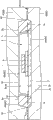
Fig. 1 shows the plane graph of the front surface side of the sensor chip that in semiconductor device according to an embodiment of the invention, comprises;
Fig. 2 is the cross-sectional view that the line A-A along Fig. 1 obtains;
Fig. 3 is the cross-sectional view that the line B-B along Fig. 1 obtains;
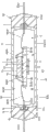
Fig. 4 shows the plane graph of the upper surface side of the semiconductor device in one embodiment of the present of invention;
Fig. 5 shows the plane graph of the lower face side of semiconductor device shown in Fig. 4;
Fig. 6 is the cross-sectional view that the line C-C along Fig. 4 obtains;
Fig. 7 is the cross-sectional view that the line D-D along Fig. 4 obtains;
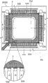
Fig. 8 shows the plane graph of the containment member of semiconductor device shown in Fig. 4 with interior planar structure;
Fig. 9 is the amplification view of the part of E shown in Fig. 8;
Figure 10 shows the key diagram of the assembling flow path figure of the semiconductor device among this embodiment of the present invention;
Figure 11 shows the plane graph that the total of the lead frame that provides in the step is provided at lead frame shown in Figure 10;
Figure 12 is that a plurality of products shown in Figure 11 form a product among the zone and form the amplification view around the zone;
Figure 13 is the amplification cross-sectional view that the line F-F along Figure 12 obtains;
Figure 14 shows the amplification view that is assemblied in the state of the semiconductor chip on the cap shown in Figure 12 (control chip) via adhesive;
Figure 15 is the amplification cross-sectional view that the line G-G along Figure 14 obtains;
Figure 16 shows the amplification view that is assemblied in the state of the semiconductor chip on the control chip shown in Figure 14 (control chip) through adhesive;
Figure 17 is the amplification cross-sectional view that the line G-G along Figure 16 obtains;
Figure 18 shows the plane graph of the state that semiconductor chip shown in Figure 16 and a plurality of lead-in wire be electrically connected via wiring;
Figure 19 is the amplification cross-sectional view that the line G-G along Figure 18 obtains;
Figure 20 shows another cap bonding and is affixed to shown in Figure 18 on the cap, is superimposed on the amplification view of the state of this cap simultaneously;
Figure 21 is the amplification cross-sectional view that the line G-G along Figure 20 obtains;
Figure 22 is the amplification cross-sectional view that the line H-H along Figure 20 obtains;
Figure 23 shows the amplification view that encapsulant is coated on the state on cap shown in Figure 18 and the lead-in wire;
Figure 24 is the amplification cross-sectional view of the corresponding Figure 23 of the cross section obtained with line H-H along Figure 20;
Figure 25 shows the amplification view that product that containment member is formed at lead frame shown in Figure 20 forms the state in the zone;
Figure 26 is the amplification cross-sectional view that the line F-F along Figure 25 obtains;
Figure 27 is the amplification cross-sectional view that the line F-F along Figure 25 obtains, and this cross-sectional view has illustrated the state of resin that supply is used to seal in the cavity of molding die;
Figure 28 is the amplification cross-sectional view of obtaining along the I-I of line shown in Figure 25, and this cross-sectional view has illustrated the state of resin that supply is used to seal in the cavity of molding die;
Figure 29 shows the amplification view of the state that the dam is cut shown in Figure 25;
Figure 30 shows that outer lead shown in Figure 29 is cut and the amplification view of the state that is shaped;
Figure 31 shows the amplification view that forms the state in zone from product shown in frame partial monosomyization (singulate) Figure 30 of lead frame;
Figure 32 is the amplification cross-sectional view that the line F-F along Figure 29 obtains, this cross-sectional view illustrated that the serving film is formed at the exposed surface of lead-in wire and the back of the body face side cap that exposes from containment member on state;
Figure 33 shows the plane graph of the lower face side of the semiconductor device in the modification example corresponding with Fig. 5;
Figure 34 is the cross-sectional view that the line C-C along Figure 33 obtains;
Figure 35 is the cross-sectional view that the line D-D along Figure 33 obtains;
Figure 36 shows the plane graph of the containment member of semiconductor device shown in Figure 33 with the planar structure on the interior upper surface side;
Figure 37 shows the cross-sectional view of the modification example of semiconductor device shown in Figure 35;
Figure 38 is the amplification view of the modification example corresponding with Figure 12;
Figure 39 is the cross-sectional view that the line F-F along Figure 38 obtains;
Figure 40 shows the amplification cross-sectional view of the modification example corresponding with Figure 21;
Figure 41 shows the front surface side can be attached to the state of lead frame after the bonding of wiring shown in Figure 10 step amplification cross-sectional view;
Figure 42 shows the amplification cross-sectional view that lead frame shown in Figure 41 is inverted the state of upset;
Figure 43 shows the amplification cross-sectional view of the modification example corresponding with Figure 26;
Figure 44 shows the plane graph of the semiconductor device in the modification example corresponding with Fig. 4;
Figure 45 shows the cross-sectional view of the semiconductor device in the modification example corresponding with Fig. 6;
Figure 46 shows the plane graph of the front surface side of the sensor chip in the modification example corresponding with Fig. 1;
Figure 47 is the cross-sectional view that the line A-A along Figure 46 obtains;
Figure 48 shows support section is assemblied in the state on the cap in the modification example corresponding with Figure 21 amplification cross-sectional view;
Figure 49 shows the amplification cross-sectional view that adhesive is coated to the state of support section shown in Figure 48;
Figure 50 shows the amplification cross-sectional view that transparent part is assemblied in the state on the support section shown in Figure 49;
Figure 51 shows the cross-sectional view of the semiconductor device in the modification example corresponding with Fig. 8;
Figure 52 shows the cross-sectional view of the semiconductor device in the modification example corresponding with Fig. 6;
Figure 53 shows the cross-sectional view of the semiconductor device in another modification example corresponding with Fig. 6;
Figure 54 shows the cross-sectional view of the semiconductor device in the modification example corresponding with Figure 45;
Figure 55 shows the cross-sectional view of the semiconductor device in the modification example corresponding with Fig. 6, Figure 45, Figure 52, Figure 53 and Figure 54;
Figure 56 shows the cross-sectional view of the semiconductor device in the modification example corresponding with Figure 34;
Figure 57 shows the amplification cross-sectional view of the comparative example corresponding with Figure 27; And
Figure 58 is the cross-sectional view of the semiconductor device in another comparative example corresponding with Figure 45.
Embodiment
(explanation of descriptor format and the implication and the use of the basic terms among the application)
Hereinafter will wait the following preferred embodiment of describing in the present patent application through if necessary then being divided into a plurality of following chapters and sections for ease, only if appointment is arranged in addition, otherwise these chapters and sections etc. are not separate.Regardless of the order of describing, each chapters and sections is the concrete part of other chapters and sections corresponding to one of each part of single example or chapters and sections or revises the some or all of etc. of example.Hereinafter will omit being repeated in this description same section in principle.Only if appointment is arranged in addition, except in theory clearly being limited to concrete number and only if based on context indication is arranged in addition, otherwise each parts of embodiment and nonessential.
Similarly, in the description of embodiment,, otherwise do not get rid of the material that comprises the key element except key element " A " about the phrase " X comprises A " of material, composition etc. only if only if appointment is arranged in addition and based on context indication is arranged in addition.For example the phrase " X comprises A " about parts means " X comprises key element " A " as critical piece ".For example term " silicon component " etc. is not limited to pure silicon.Be clear that term " silicon component " means like lower member, this member comprises SiGe (silicon and germanium) alloy or following other multicomponent alloy, and these multicomponent alloys comprise silicon as main component and other additive.Only if appointment is arranged in addition, otherwise gold plate, copper layer, nickel coating etc. not only mean the member that is formed by above-described pure material but also mean and comprise the member as main component such as gold, copper, nickel respectively.
When referring to concrete numerical value or quantity,, otherwise can use numerical value or the numerical value below concrete numerical value that surpasses concrete numerical value only if only if appointment is arranged in addition, except in theory clearly being limited to the concrete number in ground and based on context indication is arranged in addition.
In every width of cloth figure of embodiment, identical or similar part is indicated by identical or similar reference symbol or label, and will not repeat its description in principle.
In the accompanying drawings, when the hachure that is used for cross section etc. complicates cross section or when cross section, know and to omit hachure etc. when being different from the space.In this article, the closed even background profile hole also often can be omitted according to describing etc. when being understood with planar fashion.In addition, so that being cavity or clear, the clear interested part that illustrates in the accompanying drawing is not illustrated in the border between the zone even in the figure that is not cross-sectional view, hachure or dot pattern can be provided yet.
First embodiment
This embodiment will describe the example of following semiconductor device as semiconductor device, and this semiconductor device is included in the semiconductor chip of arranging in the space that is formed in the containment member.Semiconductor device have be fitted thereon and use and to be called the sensor chip (semiconductor sensor chip) that forms in the space of semiconductor microactuator process technology in being formed at containment member of " MEMS (MEMS) ".
The structure of semiconductor chip (semiconductor sensor chip)
The structure of the semiconductor chip (sensor chip) that hereinafter will use Fig. 1 to Fig. 3 to be described in to comprise in the semiconductor device of this embodiment.Fig. 1 shows the plane graph of the front surface side of the sensor chip that in the semiconductor device of this embodiment, comprises.Fig. 2 shows the cross-sectional view of obtaining along the line A-A of Fig. 1, and Fig. 3 shows the cross-sectional view of obtaining along the line B-B of Fig. 1.
The semiconductor chip of this embodiment is the sensor chip 1 that forms through the MEMS technology.The sensor chip 1 that forms through the MEMS technology comprises moveable part and is used for the mobile circuit (sensor circuit) that converts the signal of telecommunication to and send the signal of telecommunication with moveable part.Sensor chip 1 can be used for various application, for example acceleration transducer or angular-rate sensor.In this embodiment, hereinafter will be described the example of piezoresistive acceleration sensor as sensor chip.For example form sensor chip 1 through the micro-processing technology that will when making semiconductor device, use through photoetching or etching.Therefore, sensor chip 1 has the advantage that can reduce like the size of lower sensor, and this transducer comprises the moveable part that can mechanically move.For example the sensor chip 1 of this embodiment has its following front surface 1a, and the flat shape of this front surface is a rectangle, and the length on every limit for example scope be about 1mm to 10mm.
The sensor chip of this embodiment (semiconductor chip) 1 comprise front surface (first type surface) 1a, with front surface 1a mutually antidirection finding back of the body surface (first type surface) 1b and be positioned front surface 1a and the side 1c that carries on the back between the surperficial 1b.Particularly, sensor chip 1 comprises main body 1k and the lid 1n that 1m arranges on the back of the body surface of main body 1k.The back of the body surface of lid 1n becomes the back of the body surface 1b of sensor chip 1.The main body 1k of sensor chip 1 comprise from front surface 1a support or oppose opening 1d that surperficial 1m penetrates, be arranged in supporting member (frame part) 1e around the opening 1d and vertical (plumb) that be arranged in the opening 1d and support by supporting member 1e via a plurality of beams part (beam) 1f (moveable part) 1g partly.
The main body 1k of sensor chip 1 is for example processed by silicon, and forms supporting member 1e, beam part 1f and vertical component 1g.The a plurality of beam part 1f that are used to support vertical component 1g are for flexible.When apply to beam part 1f with by the interested external force (for example inertia force or gravity) of sensor chip 1 sensing when moving vertical component 1g, crooked (flexibly distortion) beam part 1f.Pressure drag component is arranged on each beam part 1f.Each pressure drag component is electrically connected with each pad among a plurality of pads that are formed at front surface 1a (electrode pad or the bonding welding pad) 1h via the wiring (not shown) that is formed in the sensor chip 1.Pressure drag component is the resistive element that its resistance changes according to stress.That is to say; Sensor chip 1 is following acceleration transducer, and this acceleration transducer uses the resistance owing to due to the bending of beam part 1f of the pressure drag component that is arranged in each beam part 1f to change so that the resistance change is converted to the signal of telecommunication, obtains the signal of telecommunication from pad 1h then.As mentioned above, sensor chip 1 comprises the moveable part (vertical component 1g) mechanically operated according to the interested external force of treating sensing, be used for another circuit (being formed at wiring (not shown) or the pad 1h of supporting member 1e) that the operation of moveable part is converted to the circuit (pressure drag component of beam part 1f) of the signal of telecommunication and is used for sending electrical signal converted.
The operation of sensor chip 1 detection moveable part as mentioned above is as the signal of telecommunication.From the viewpoint of the reliability of transducer, importantly (reference position) is provided with vertical component 1g and at bent beam part 1f not when transducer applies the interested external force of treating sensing not in the precalculated position.From this viewpoint, the semiconductor device (semiconductor packages) that sensor chip 1 is incorporated into wherein preferably reduces the external force except that the interested external force of treating sensing that applies to the major part 1k of sensor chip 1 when possible.Therefore, in this embodiment, shown in Fig. 2 and Fig. 3, lid 1n is not arranged on the front surface 1a and beam part 1f is arranged on the front surface 1a in major part 1k.As described in hereinafter, the containment member of semiconductor device is with interior formation space, and sensor chip 1 is arranged in this space.
The schematic construction of semiconductor device
Then hereinafter will use Fig. 4 to Fig. 9 to describe the example of structure of the semiconductor device of this embodiment.Fig. 4 shows the plane graph of the upper surface side of the semiconductor device among this embodiment.Fig. 5 shows the plane graph of the lower face side of semiconductor device shown in Fig. 4.Fig. 6 is the cross-sectional view that the line C-C along Fig. 4 obtains.Fig. 7 is the cross-sectional view that the line D-D along Fig. 4 obtains.Fig. 8 shows the plane graph of the containment member of semiconductor device shown in Fig. 4 with interior planar structure.Fig. 9 is the amplification view of the part of E shown in Fig. 8.Fig. 8 and Fig. 9 show the internal structure of semiconductor device transparent flat figure, be specially and show the plane graph that passes the internal structure that containment member shown in Fig. 49 and cap 5 check.Fig. 6 to Fig. 8 has omitted the diagram of concrete structure of sensor chip 1 (structure shown in Fig. 1 to Fig. 3) with easy to understand.
The semiconductor device of this embodiment is to use lead frame as substrate semiconductor chip to be assemblied in the lead frame semiconductor package on the chip assembled portion.In this embodiment, hereinafter will be described four limit flat packaging (QFP) 10 through example, and this QFP is the type semiconductor devices of lead frame shown in Fig. 5.Develop the technology that is used to reduce cost for a good while and can be applied to the lead frame type semiconductor devices.Owing to can use the infrastructure (such as making equipment) of having constructed, so compare the manufacturing cost that can reduce the lead frame type semiconductor devices with the substrate-type semiconductor device of assembling semiconductor chips on wiring plate.
Hereinafter will be described the overview of the structure of QFP shown in Fig. 4 to Fig. 9 10.Shown in Fig. 6 and Fig. 7, QFP 10 comprises cap (first member or carry on the back face side cap material) 2, and this cap has upper surface 2a, lower surface 2b and the side 2c upper surface 2a and lower surface 2b between opposite with upper surface 2a.Cap 2 is tabular components of being processed by metal material.QFP 10 comprises the sensor chip 1 as using Fig. 1 to Fig. 3 to describe.Sensor chip 1 is assemblied on the upper surface 2a of cap 2 and to carry on the back the upper surface 2 of surperficial 1b and cap 2 relative.In example shown in Fig. 4 to Fig. 9, QFP 10 incorporates control chip (controller chip) 6 controlled sensor chip 1 as being used among the QFP 10 semiconductor chip into.Sensor chip 1 is assemblied on the control chip 6.QFP 10 comprises and is arranged in sensor chip 1 (with control chip 6) a plurality of lead-in wires (terminal) 3 on every side.QFP 10 has a plurality of wiring 4 that lead-in wire 3 is electrically connected with the pad 1h of sensor chip 1.As mentioned above, QFP 10 also comprises control chip 6 except sensor chip 1.Shown in Fig. 6 and Fig. 9, the pad 1h of sensor chip 1 is electrically connected with the pad 6d of control chip 6 via wiring 4a.The pad 6e of control chip 6 comes to be electrically connected with lead-in wire 3 via wiring 4b.Pad 6d and pad 6e are electrically connected via the wiring (not shown) that in control chip 6, provides.That is to say that in QFP 10, the pad 1h of sensor chip 1 is electrically connected with lead-in wire 3 via wiring 4a and 4b and control chip 6.Shown in Fig. 6 and Fig. 7, QFP 10 comprises cap (second member or front surface side cap material) 5, and this cap has upper surface 5a, lower surface 5b and the side 5c upper surface 5a and lower surface 5b between opposite with upper surface 5a.Cap 5 has towards the concave shape of upper surface 5a.Cap 5 has cavity (space forms part, recessed portion, sunk part or chip holding portion) 5d and flange (bonding part) 5e that is arranged to surround cavity 5d on its lower surface 5b side.Cap 5 is arranged on the upper surface 2a of cap 2, thereby 3 the some parts of going between (wiring 4 is by the bonding of bonding zone), sensor chip 1 and wiring 4 are positioned at cavity 5d.(zone between the upper surface 2a of the adhesive surface 5f of flange 5e and cap 2) is by encapsulant 7 sealings in the bonding part between cap 2 and the cap 5.That is to say that through stack cap 2 is to be bonded together these caps on cap 5, the space 8 in the cavity 5d becomes the hollow space to external world's sealing.In space 8, arrange some parts, sensor chip 1 and the wiring 4 of lead-in wire.In addition, QFP 10 containment member (resin component element) 9 that is included in the bonding part between cap 2 and 5 and is used for other part (except as the zone of inner lead portion 3a beyond cap 2 and 5 the external lead portion 3b of external terminal) of sealing wire 3.That is to say that QFP 10 is following semiconductor device, this semiconductor device in containment member 9, forms space 8 and it is included in the sensor chip 1 that is arranged as semiconductor chip in the space 8.
In QFP 10 shown in Fig. 6 and Fig. 7, the side 2c of cap 2 and the side 5c of cap 5 are covered by containment member 9, and expose the lower surface 2b of cap 2 and the upper surface 5a of cap 5 fully from containment member 9.In other words, in plane graph shown in Fig. 4, containment member 9 is not arranged in circumference or its circumference of upper surface 5a of cap 5.In another plane graph, as shown in Figure 5, containment member 9 is not arranged in circumference or its circumference of lower surface 2b of cap 2.With specifically described, in this embodiment, the entire upper surface 5a of whole lower surface 2b and cap 5 that exposes cap 2 is to reduce in the step of formation containment member 9 to cap 2 and 5 applied pressures like back literary composition, and this can suppress the distortion of cap 5 in cavity 5d.Utilize this layout, the sealed nature that can keep space 8 invades in the space 8 to prevent or to suppress containment member 9.Thereby the sensor chip 1 due to the stress influence of this embodiment containment member 9 that can suppress to produce owing to sensor chip 1 contact seal member 9 etc. and the reliability of QFP 10 reduce.Sentence " exposes entire upper surface 5a and whole lower surface 2b from containment member 9 " and means from the major part of containment member 9 exposed upper surface 5a and lower surface 2b.This means and do not get rid of following situation.For example in the step that forms containment member 9, resin burr etc. is created on the border between upper surface 5a or lower surface 2b and containment member 9 and covers upper surface 5a slightly or lower surface 2b.Similarly, sentence " containment member 9 is not arranged in circumference or its circumference of upper surface 5a (lower surface 2b) " means the resin (such as the resin burr) that for example removal stays slightly and containment member 9 is not arranged in here.Term " resin burr " mean resin (being specially thermosetting resin) (resin that is used for sealing) follow-up sealing step spill and the thickness of resin very little in cross-sectional view or end view.
The concrete structure of semiconductor device
Hereinafter will be described in the concrete structure of each parts that comprises among the QFP 10 now.Cap 2 is included in as shown in Figure 8 to have the flat board of rectangular shape in the plane graph and not to have big sunk part (cavity formation part) (as the cavity 5d of cap 5 shown in Fig. 6 and Fig. 7).The length of one side of cap 2 for example is about 15nm to 20nm.In this embodiment, the viewpoint in crack appears in the interface from be suppressed at containment member 9 between containment member 9 and cap 2, four turning chamferings (receiving R technology) of cap 2.The flat shape of cap 2 is not limited to form shown in Fig. 8, and can for example be the not rectangular planar shape of chamfering of its turning.In order on following (assembly surface) side of QFP 10, to expose the lower surface 2b of cap 2, cap 2 is thicker than cap 5.Cap 5 for example has the thickness that is about 0.2mm to 1mm.From the viewpoint of the intensity that improves cap 2, cap 2 is thick more, and the intensity of cap 2 is just good more.Under this situation, it is very thick that the gross thickness of QFP 10 becomes.Therefore this embodiment can reduce cap 2 needed intensity own through reducing the distortion that suppresses cap 2 to cap 2 applied pressures.As long as just can make the thickness attenuation of cap 2 from the lower surface of containment member 9 exposure caps 2.For example can form cap 2 by the thickness identical with the thickness of cap 5.
In QFP 10, cap 2 is suitable for as being used for control chip 6 is assemblied in the chip assembled portion on it.In other words, control chip 6 is assemblied on the upper surface 2a as the cap 2 of chip assembled portion via adhesive (die bonding material) 11.Control chip 6 has front surface 6a, the back of the body opposite with front surface 6a surface 6b and is positioned front surface 6a and the side 6c that carries on the back between the surperficial 6b.Assemble control chip 6 through so-called facing up, thereby the upper surface 2a that carries on the back surperficial 6b and cap 2 is relative.Adhesive 11 is not limited to concrete material, and can other material that control chip 6 is fixed to the upper surface 2a of cap 2 be processed by any.In this embodiment, control chip 6 for example comprises that through applying the paste resin binder of epoxy thermosetting resin comes bonding, and thermmohardening is with set then.Sensor chip 1 is assemblied on the surperficial 6a of control chip 6 via adhesive 12.That is to say that sensor chip 1 is assemblied on the control chip 6 through facing up.Adhesive 12 also is the member that is used for semiconductor chip 1 is fixed to control chip 6.From suppressing since adhesive 12 (part of this adhesive is attached to the side 1c (see figure 2) of sensor chip 1) the stress of generation cause characteristic (sensed characteristic) to sensor chip 1 such viewpoint that has a negative impact, adhesive 12 is preferably membranaceous jointing material.Why film adhesive is preferably because it still less possibly be attached to the side 1c of sensor chip 1 than paste-type adhesive.Film adhesive for example is called die attach (DAF) and can is following adhesive, and this adhesive generally is used as the adhesive that is used at second half conductor chip of semiconductor chip laminated.
Be similar to QFP 10; In the time of on semiconductor chip 1 is assemblied in cap 2; From reducing the such viewpoint of stress influence that generates owing to the linear expansion coefficient difference between cap 2 and sensor chip 1, cap 2 is preferably processed by the approaching material of linear expansion coefficient of linear expansion coefficient and sensor chip 1.Therefore, in this embodiment, sensor chip 1 is for example processed by silicon, and cap 2 processed by Kovar (a kind of comprise the nickel that adds to iron and the alloy of cobalt), and this material is the approaching metal material of the linear expansion coefficient of linear expansion coefficient and silicon.Be similar to cap 2, cap 5 also comprises Kovar.Particularly, the film that is coated with that for example comprises nickel or nickel and palladium is formed on the surface (the upper surface 5a of the upper surface 2a of cap 2 and lower surface 2b or cap 5, lower surface 5b and side 5c) of the substrate that comprises Kovar.Nickel and palladium mean and comprise that being used to form of following alloy is coated with the material of film that this alloy comprises nickel (Ni) and palladium (Pd).Hereinafter is described as nickel palladium or Ni/Pd with the alloy of nickel and palladium and will comprises that the film that is coated with of nickel palladium is described as nickel palladium film.The film (nickel film or nickel palladium film) that is coated with that comprises nickel or nickel palladium is suitable for as being used to prevent that the oxidation of cap 2 and 5 oxidations from preventing film.The film (nickel film or nickel palladium film) that is coated with that is formed on the side 5c of cap 5 is suitable for as the adhesiveness raising film that is used to improve the interfacial adhesion between containment member 9 and cap 5.From reducing the viewpoint that transmits stress to sensor chip 1, sensor chip 1 directly is not assemblied on the cap 2 and preferably is assemblied in (as QFP 10) on the cap 2 via the control chip that comprises silicon 6.This can further reduce the stress that transmits to sensor chip 1.Cap 2 among this embodiment has the plate portion that does not receive bending process.That is to say that be different from the back literary composition with the cap of describing 5, cap 2 does not receive bending process, so cap 2 can have the intensity lower than the intensity of cap 5.Therefore, cap 2 can comprise and the material identical materials (copper or copper alloy) that is fixed to the lead-in wire 3 of cap 2 via adhesive 7.Situation as using Kovar under this situation, for example comprises that the film that is coated with of nickel or nickel palladium also preferably is formed on the surface (the upper surface 5a of the upper surface 2a of cap 2 and lower surface 2b and cap 5, lower surface 5b and side 5c) of substrate.
Owing in this embodiment, expose the lower surface 2b of cap 2, cap 2 can be suitable for as the radiating component (radiator) that is used for being dissipated in addition to QFP 10 heat of space 8 generations.From the viewpoint of heat radiation route, cap 2 comprises the metal that the thermal conductivity of thermal conductivity ratio ceramic material is higher, therefore compares with ceramic packaging and can improve radiating efficiency.When using cap as radiating component, the grafting material (not shown) (such as scolder) that for example is made of metal is arranged on the lower surface 2b side of cap 2, thereby cap 2 can join the terminal (not shown) of assembling substrate (not shown) through the knot material to.Under this situation, can make to the heat transfer of assembling substrate more efficiently, therefore improve radiating efficiency.
A plurality of lead-in wires (terminal) 3 are arranged in around sensor chip 1 and the control chip 6.Lead-in wire 3 is external terminals of QFP 10, and each lead-in wire comprise be arranged in containment member 9 with interior inner lead portion 3a (inside that comprises space 8) be arranged in lead member 9 external lead portion 3b in addition.Inner lead portion 3a and external lead portion 3b form each other.Each lead-in wire 3 for example comprises copper or copper alloy and for example on its surface (upper surface, lower surface and side (being positioned the surface between the surface, up and down)), has by what nickel or nickel palladium formed and is coated with film (metal film).Being coated with film can be formed on the whole surface of each lead-in wire 3.When being coated with film when not being formed on the whole surface of lead-in wire, another is coated with film (being coated with film outward) connects material by lead welding or be substantially free of lead on the surface (upper surface, lower surface and side) of the external lead portion 3b that exposes from containment member 9 after forming containment member 9 welding material (lead-free solder) and forms.The 3b of external lead portion shown in Fig. 6 is arranged to give prominence to from the side of containment member 9 and beyond containment member 9, receive bending process.For example Fig. 6 shows the example of gull wing form.The 3a of inner lead portion shown in Fig. 6 is from extending to space 8 with the border of external lead portion 3b and letting its top be contained in the space 8.Because inner lead portion 3a is arranged in the space 8, so the top of inner lead portion 3a (zone of bonding shown in Figure 13 3c) is arranged on the upper surface 2a of cap 2.In this way, the part of inner lead portion 3 is arranged in the space 8, thereby the bonding part that is used for control chip is coupled to lead-in wire 3 wiring 4b can be arranged in the space 8 (cavity 5d).That is to say that the zone that centers on around the top of inner lead portion 3a becoming the bonding zone that is used to engage wiring 4b.Can use cap 5 to cover wiring 4b at cavity 5d with the interior bonding zone that provides.As mentioned above, cap 2 comprises metal material (conductive material) (such as Kovar, copper or copper alloy).Therefore, if the lead-in wire 3 that is arranged on the cap 2 does not insulate with cap 2, then will between lead-in wire 3, cause short circuit.Therefore, QFP 10 has the insulating binder 13 between the lower surface of the upper surface 2a that is arranged in cap 2 and lead-in wire 3, and go between 3 by adhesive 13 bondings be affixed to cap 2.
In plane graph shown in Fig. 8, arrange lead-in wire 3 along four limits of QFP 10 respectively.Sensor chip 1 and control chip 6 are with reference to having rectangular planar shape respectively with the semiconductor chip, and go between 3 in plane graph on the position with four limit positioned opposite.In example shown in Fig. 8 and Fig. 9, arrange a plurality of pad 6e (see figure 9)s along the both sides respect to one another among four limits of control chip 16, and wiring 4b is coupled to the lead-in wire 3 relative with pad 6e.Other lead-in wire 3 relative with the limit of no any pad 6e of rectangle control chip is not coupled to wiring 4.Therefore, when lead-in wire 3 number during greater than terminal (pad) number of semiconductor chip, some lead-in wires 3 can be configured to not be coupled to wiring 4.In QFP 10 shown in Fig. 8 and Fig. 9, the pad 1h (see figure 9) of sensor chip 1 is not directly coupled to lead-in wire 3 via wiring 4.That is to say that the pad 1h that is coupled to wiring 4 among the pad 1h of sensor chip 1 is coupled to the pad 6d (see figure 9) of control chip 6 via all wiring 4a.The lead-in wire that is coupled to wiring 43 among lead-in wire 3 is coupled to the pad 6e of control chip 6 via all wiring 4b.In this way, the pad 1h of sensor chip 1 is coupled to lead-in wire 3 via control chip 6, and this can shorten the length of the wiring 4a that is coupled to pad 1h.For example shown in Fig. 6 and Fig. 8, the length of wiring 4a is shorter than the length of wiring 4b.As shown in Figure 6, when wiring 4 was arranged in the space 8, the external force that wiring 4 is often generated by the vibration that applies to QFP 10 etc. was vibrated.Particularly, when the wiring 4a of sensor chip 1 is coupled in violent oscillatory motion, the characteristic of sensor chip 1 (sensed characteristic) will be degenerated.When QFP 10 externally applied forces are constant, reduce the degree of vibration through the length that reduces wiring 4.For the characteristic (sensed characteristic) that suppresses sensor chip 1 descends, the pad 1h that is coupled to wiring 4 among the pad 1h of sensor chip 1 preferably is coupled to the pad 6d of control chip 6 through all wiring 4a.The layout of wiring is not limited to form shown in Fig. 8 and Fig. 9, but can make various modifications to terminal (pad) number and the layout that are coupled to lead-in wire 3 of semiconductor chip.
Cap (second member or front surface side cap) 5 is arranged on control chip 6 and the sensor chip 1.Cap 5 shown in Fig. 6 and Fig. 7 comprise upper surface 5a, the lower surface 5b opposite with upper surface 5a and be positioned upper surface 5a and lower surface 5b between side 5c.Cap 5 comprises Kovar and lets its surface (upper surface 5a, lower surface 5b and side 5c) covered by the film that is coated with that nickel forms.Basically be arranged on the lower surface 5b side of cap 5 at the cavity 5d of the center arrangement of cap 5 and flange (bonding part) 5e of surrounding cavity 5d.In QFP10, the flange 5e of cap 5 joins the circumference of the upper surface 2a of cap 2 to via encapsulant 7 (with adhesive 13), thereby sensor chip 1, control chip 6, wiring 4 and 3 the appropriate section (bonding zone) of going between are sealed in the space 8.The degree of depth of cavity 5d is greater than the thickness of semiconductor chip (sensor chip 1 and control chip 6), and is still preferably thin as far as possible so that make encapsulation thinner, because the thickness of the effect of depth QFP 10 of cavity 5d.For example in this embodiment, the depth bounds of chamber 5d is about 1mm to 3mm.The planar dimension of cavity 5d is greater than the planar dimension of each chip in sensor chip 1 and the control chip 6.For example in plane graph, form rectangle chamber 5d an edge lengths for example scope be about 13mm to 18mm.
Encapsulant 7 is members of arranging in the bonding part between cap 2 and cap 5.In order to improve the sealed nature in space 8, require encapsulant 7 to have high sealing character (the embedding character between adjacent legs 3, from the coating time to bonding and the bond property of the shape keeping property of set time and bonded interface).In this embodiment, high sealing character desired seal material 7 is preferably formed by following material.That is to say; From reducing the viewpoint in the gap between adjacent legs 3, encapsulant 7 is preferably formed by the material (as membranaceous (band shape) adhesive (for example jointing material (such as adhesive 12))) that before sclerosis, has the material of paste character rather than under solid state, be bonded to object.The encapsulant 7 that applies need be when applying encapsulant 7 time during to sclerosis encapsulant 7 to the shape that keeps it.Therefore, encapsulant 7 preferably has high viscosity on a certain degree.For example has the coating shape that low-viscosity encapsulant (as water) can not keep it.Contrast when the viscosity of encapsulant is too high, possibly generate the gap between adjacent legs 3.Encapsulant 7 preferably has so low viscosity, and this viscosity makes and can 3 harden then to be fixed on its coating shape of maintenance in the bonding part between cap 2 and 5 being coated to cap 2 and going between.For example in this embodiment, use following adhesive to form adhesive 11 and encapsulant 7, this adhesive comprises the epoxy thermosetting resin that contains filler (particle).Encapsulant 7 is lower than the viscosity of adhesive 11 before sclerosis in the viscosity before the sclerosis.The ratio of components (such as the bonding agent that is used to regulate viscosity) of shape that can be through regulating the filler that adds to adhesive or particle diameter, adhesive waits carries out such viscosity adjustment.After sclerosis encapsulant 7, require sealing and be fixed on cap 2 and 5 with the bonding interface that is used for that goes between between 3.In this embodiment; The film of being processed by same metal material (for example nickel or nickel palladium) that is coated with is formed on the adhesive surface 5f and each surface in 3 the surface of going between of flange 5e of upper surface 2a, cap 5 of cap 2, and this can easily improve and the adhesiveness that is arranged in each parts in the bonding part.Note being used for lead-in wire 3 bondings and the adhesive 13 that is affixed to the upper surface 2a of cap 2 also are arranged in the bonding part.Therefore also can use with encapsulant 7 identical materials and form adhesive 13.For example when the paste thermosetting resin when the encapsulant 7, even use film adhesive to be filled in the gap between the adjacent legs 3 as adhesive 13 usefulness encapsulants 7.Therefore, in this embodiment, adhesive 13 is the film adhesive (for example on the surface of membranaceous substrate, as adhesive 12) that are easy to handle.
Then, the bonding part between cap 2 and 5 is covered by containment member 9.Containment member 9 is the resins that generally in being called the resin-sealed semiconductor device of " Plastic Package ", use.In this embodiment, form containment member 9 through transmitting molded (hereinafter will specifically describe).As shown in Figure 6, in QFP 10, each semiconductor chip (sensor chip 1 with control chip 6) is arranged in the space 8 that forms through the cap 2 that on cap 5, superposes with the wiring 4 of being coupled to this semiconductor chip.The structure of no containment member 9 also is regarded as the modification example.Yet when not forming containment member 9, the bonding part between cap 2 and 5 is exposed, therefore the for example fracture easily owing to impact the perhaps hot external force that influence generated.In order to suppress the fracture of bonding part, be intended to increase the intensity of encapsulant 7 and adhesive 13, this will make the sealed nature in space 8 degenerate.Its manufacturing step will be complicated.As shown in Figure 6, preferably, the outside of the bonding part between the cap 2 and 5 is by containment member 9 coverings and protection.Select most optimum materials to form encapsulant 7 and adhesive 13 through considering above-mentioned sealed nature.The bonding part is reinforced by containment member 9, and this compares the fracture that can suppress the bonding part with the situation that does not form containment member 9.
As shown in Figure 8, containment member 9 has the rectangular shape that comprises four limits (the main limit except the turning of chamfering) in plane graph.Each suspended lead 14 is arranged in the turning that corresponding edge intersects.The limit 14 that suspends is following supporting members, and this supporting member is used for after the back literary composition is forming containment member 9 with the manufacturing process of the QFP 10 that describes, in each step of singulation QFP 10, supporting containment member 9 with interior zone through lead frame as substrate.Therefore, suspended lead 14 comprises and lead-in wire 3 identical materials (for example copper or copper alloy) separately.Contrast, in this embodiment, each in the cap 2 and 5 for example comprises Kovar As mentioned above and opened formation in 14 minutes with suspended lead.As mentioned above, cap 2 can comprise and lead-in wire 3 identical materials (for example copper or copper alloy).Production process of semiconductor device
Then hereinafter will be described the manufacturing process of QFP 10 with reference to Fig. 5 to Fig. 9.Figure makes QFP 10 according to assembling flow path shown in Figure 10.Figure 10 shows the key diagram of assembling flow path figure of the semiconductor device of this embodiment.Hereinafter will use Figure 11 to Figure 31 to specifically describe each step.
1. lead frame provides step: Figure 11 shows the plane graph that the total of the lead frame that provides in the step is provided at lead frame shown in Figure 10, and the product that Figure 12 shows among product shown in Figure 11 forms the zone forms zone amplification view on every side.Figure 13 is the amplification cross-sectional view that the line F-F along Figure 12 obtains.
At first, provide in the step, lead frame 20 is provided as shown in Figure 11 at lead frame shown in Figure 10.The lead frame 20 that in this embodiment, uses comprises that being arranged in frame part (framework) 20b forms regional 20a with interior product.Arrange that by row and row product forms regional 20a.Frame part 20b is arranged in adjacent products and forms between the regional 20a.Form between the regional 20a along the regional 20c of line direction layout running channel (runner) in adjacent products.Running channel zone 20c is the zone that has like down sprue, and these running channels are arranged to be suitable for form the supply route of resin that cavity in regional 20a be provided for seal in follow-up sealing step to being arranged in each product as being used for.
Shown in Figure 12 (this figure is the part enlarged drawing of Figure 11), cap 2 is arranged in the center that each product forms regional 20a.Generally speaking, in the manufacturing step of lead frame type semiconductor devices, pipe core welding disc (groove seat (tub)) (being used for semiconductor chip is assemblied in the chip assembled portion on it) is arranged in the center that product forms the zone.Pipe core welding disc is coupled to the frame part of lead frame via suspended lead.Therefore yet in this embodiment, cap 2 also is suitable for as the chip assembled portion, does not form the pipe core welding disc that forms with lead frame in the association area.In this embodiment, cap 2 is formed by the material material different with lead frame 20.For example lead frame 20 is processed by metal (in this embodiment, for example being copper (Cu) or copper alloy).Particularly, as shown in Figure 13, be coated with film (metal film) 22 and on the surface of the substrate 21 that comprises copper (Cu), for example form by nickel (Ni) or nickel palladium (Ni/Pd).In cap 2, for example comprise that the film (metal film) 22 that is coated with of nickel (Ni) or nickel palladium (Ni/Pd) for example is formed on the surface of the substrate 23 of being processed by Kovar.Therefore, cap 2 was opened formation in 20 minutes and is gone between 3 via adhesive 13 bondings with being affixed to lead frame.At this moment, comprise nickel or nickel palladium (Ni/Pd) be coated with film 22 be formed at lead-in wire 3 and and cap 2 in each and adhesive 13 between adhesive interface on, this can improve the adhesiveness with adhesive 13.In this step, as shown in Figure 12, following lead frame 20 is provided, lead-in wire 3 is with cap 2 bondings and be affixed to this lead frame.In describing hereinafter, particularly, except when being different from cap 2 and describing, lead frame 20 comprises bonding and the cap 2 that is affixed to lead-in wire 3.
As shown in Figure 12, lead-in wire 3 is arranged in around the cap 2.Lead-in wire 3 is included in separately as shown in Figure 6 to be accomplished when forming by the inner lead portion 3a of containment member 9 sealings and the external lead portion 3b that exposes from containment member 9.As shown in Figure 13, lead 3a comprises bonding zone 3c, sealing area 3d and the sealing area 3e that arranges successively from the inner of each lead-in wire 3.Outer lead 3b comprises from the dam zone 3f and the outermost regions 3g that arrange successively with the border of lead 3a.Bonding zone 3c is arranged in the inner of lead-in wire 3.Bonding zone 3c is the zone that is used in wiring bonding step (see figure 10) bonding wiring 4 (see figure 6)s.Sealing area 3d is arranged between bonding zone 3c and the outer lead 3b.In the step (see figure 10) of cap interval, sealing area is the zone by the sealing of encapsulant 7 (see figure 6)s between flange 5e (see figure 6) that is positioned cap 5 and the sealing area itself.Sealing area 3e is arranged between sealing area 3d and the external lead portion 3b and is the zone that in sealing step (see figure 10), is sealed by containment member 9 (see figure 6)s.Dam zone 3f is arranged in the zone between sealing area 3e and the outermost regions 3g and is coupled to dam 24 (seeing Figure 12), and dam 24 will be suitable in sealing the step (see figure 10) when the resin that the molding die supply is used to seal as the dam.Outermost regions 3g is positioned at the outer end of lead-in wire 3.Outermost regions 3g receives bending process for example to become the zone of the wing shape of gull as shown in Figure 6 in lead-in wire formation step (see figure 10).
Each dam (dam burr or shunt bar (tie bar)) 24 is arranged to extend between the dam zone 3f (seeing Figure 13) of lead-in wire 3 shown in Figure 12, to intersect (orthogonal directed with lead-in wire 3) with lead-in wire 3.Lead-in wire 3 forms via dam 24 and lead frame 20.Dam 24 is arranged to surround cap 2.In the sealing step (see figure 10) that the back literary composition will be described, the resin that supply is used to seal in dam 24 area surrounded is to form containment member shown in Fig. 69 thus.Suspended lead 14 is arranged in each turning of the rectangle of dam 24 formation.In other words, lead-in wire 3 is arranged between the adjacent suspended lead 14.Suspended lead 14 is like lower member, and this member is used for making product form regional 20a until singulation step afterwards at the outermost regions 3g (seeing Figure 13) of the formation of lead-in wire shown in Figure 10 step cutting lead 3 to be supported by lead frame 20 with each interior parts.Therefore, suspended lead 14 forms with lead frame 20.
Can for example form lead frame shown in Figure 11 to Figure 13 20 with the following methods.At first provide the thin plate processed by copper (Cu) with thus through etching with for example as shown in Figure 12 pattern form lead-in wire 3, suspended lead 14 and dam 24.The number that forms regional 20a with product shown in Figure 11 provides cap 2 accordingly, and adhesive 13 is arranged in the circumference of upper surface 2a.And be arranged in the zone on the upper surface 2a of cap 2 through brigadier's cap 2 being bonded to lead-in wire 3 so that at the adhesive 13 wherein of superposeing on lead-in wire 3 the apex zone (zone 3c of bonding shown in Figure 13 and sealing area 3d).Then for example go between 3 thus cap 2 is fixed to through heating lead frame 20 (cap 2 is bonded to this lead frame) curing adhesive 13.At this moment in order to improve the sealed nature in space shown in Fig. 68, adhesive 13 importantly is set in order to avoid between the upper surface 2a of the lower surface of lead-in wire 3 and cap 2, generate the gap.Under the situation of paste-type adhesive, when the amount of adhesive 13 was excessive, the part of adhesive 13 occurred towards the upper surface side (Figure 13) of bonding zone 3c, causes fault in this bonding in wiring bonding step (see figure 10).Therefore preferably use film adhesive (being specially the upper surface and the adhesive layer on the lower surface (jointing material that for example comprises thermoset resin layer) that are positioned as the resin molding of substrate) to form adhesive 13.
As mentioned above, the number that forms regional 20a with product shown in Figure 11 provides cap 2 accordingly, then cap 2 is aimed at lead-in wire 3.Yet can use various modification examples.For example can use following modification.That is to say, cap 2 be coupled integratedly via the suspended lead (not shown) suspended lead of cap (be used to be coupled) so that cap 2 bondings be affixed to lead-in wire 3, cut suspended lead then.Under this situation, be arranged in the cap 2 that product forms among the regional 20a and can aim at fully each other with lead-in wire 3.In addition because the space that need be used to cut the suspended lead (not shown) that cap 2 is coupled, so the suspended lead 14 that forms with lead frame 20 is preferably arranged apart with cap 2.Therefore, can in the space between suspended lead 14 and the cap 2, cut and be used for suspended lead (not shown) that cap 2 is coupled.When the cap that is not coupled 2 bondings be affixed to lead-in wire 3 the time, in the modification example corresponding with Figure 12, suspended lead 14 can bonding and the upper surface 2a side that is affixed to each cap 2 (as going between 3).
2. semiconductor chip provides step:
Providing at semiconductor chip shown in Figure 10 provides the semiconductor chip shown in Fig. 6 (semiconductor chip 1 with control chip 6) in the step.In this step, following semiconductor wafer (not shown) is provided, this semiconductor wafer comprises a plurality of chip areas and for example comprises silicon.Divide semiconductor wafer to obtain the semiconductor chip of a plurality of kinds thus through the dicing blade (not shown) of advancing along the scribe line of semiconductor wafer subsequently.Particularly; Following semiconductor wafer is provided, and this semiconductor wafer is included in the transducer (moveable part) that comprises in the sensor chip 1 in respective chip shown in Fig. 1 to Fig. 3 zone and is electrically connected with moveable part and the sensor circuit part through the formation of MEMS technology.Another following semiconductor wafer is provided in each chip area, and this semiconductor wafer is included in the control circuit that comprises in the control chip 6 among Fig. 6 to Fig. 8.Each semiconductor wafer of singulation, thus sensor chip 1 and control chip 6 obtained.In this embodiment, sensor chip shown in Fig. 61 is assemblied on the surperficial 6a of control chip 6 via film adhesive (for example DAF).Adhesive 12 is attached to the back of the body surface 1b of each sensor chip 1 that in this step, obtains.
3. semiconductor chip assembles step
Figure 14 shows semiconductor chip (control chip) is assemblied in the state on the cap shown in Figure 12 via adhesive amplification view.Figure 15 is the amplification cross-sectional view that the line G-G along Figure 14 obtains.Figure 16 shows semiconductor chip (sensor chip) is assemblied in the state on the control chip shown in Figure 14 via adhesive amplification view.Figure 17 is the amplification cross-sectional view that the line G-G along Figure 16 obtains.Figure 14 and Figure 16 show cap shown in Figure 12 2 enlarged drawing on every side with easy to understand.
In the assembling of semiconductor chip shown in Figure 10 step, control chip 6 is assemblied on the upper surface 2a of cap 2 with the order of sensor chip 1 shown in Figure 14 to 17 then.In this step, shown in Figure 14 and Figure 15, control chip 6 (this control chip is the semiconductor chip that is arranged as lower floor) is assemblied on the upper surface 2a of cap 2 via adhesive 11.In this embodiment, as shown in Figure 14, pad 6d and 6e are formed at respectively on the both sides respect to one another among four limits that in surperficial 6a, comprise.In this step, the both sides of pad 6e of wherein arranging control chip 6 along center that the corresponding edge of cap 2 is arranged in cap 2 so that relative with bonding respectively with the one group of lead-in wire that is affixed to cap 2 (lead-in wire 3).As shown in Figure 15, carry out the so-called assembling that faces up, thereby the back of the body of control chip 6 surface 6b is assembled into relative with the upper surface 2a of cap 2.
In this embodiment, through the adhesive 11 assembling control chips 6 that for example comprise the epoxy thermosetting resin.Adhesive 11 is to have flexible paste material before in sclerosis (hot curing).When using the paste material, at first apply paste-type adhesive 11 to the chip assembly area of the upper surface 2a of cap 2 as adhesive 11.For example offset then and promote to push shown in Figure 15 anchor clamps 30, adhesive 11 is launched and to be bonded to this back of the body surperficial on the surperficial 6b of the whole back of the body of control chip 6 with the back of the body surface 6b that the upper surface 2a with cap 2 offsets and pushes control chip 6 through front surface 6a with control chip 6.At bonding curing adhesive 11 (for example receiving heat treatment) afterwards, thereby control chip 6 is affixed to chip assembly area 2d through adhesive 11 shown in Figure 14 and Figure 15.In revising example, adhesive 11 can be a film adhesive.Consider to improve heat radiation, can use the adhesive that comprises the high conductive particles of thermal conductivity towards cap 2.Paste-type adhesive is why preferably because adhesive can improve the bond strength with the upper surface 2a of the cap 2 that comprises metal (for example nickel or nickel palladium).In this way, use paste-type adhesive 11 on the surperficial 6b of the whole back of the body of control chip 6, to launch adhesive 11, thereby outwards expand from the outer of control chip 6 shown in the outer of adhesive 11 such as Figure 14 and Figure 15.For the reliability that suppresses the QFP (see figure 6) reduces, the front surface 6a side that the part that importantly prevents adhesive 11 becomes wet and rises to control chip 6 perhaps arrives sensor chip 1 (see figure 6) to cover pad 6d with 6e.Therefore, as long as adhesive 11 becomes wet and on the surperficial 6b of the whole back of the body of control chip 6, launches, the amount of the layout of adhesive 11 (amount of coating) is preferably little so.The viscosity of adhesive 11 increases on a certain degree can prevent that adhesive 11 from becoming wet and rising to surperficial 6a side.Therefore, adhesive 11 is higher than the viscosity of adhesive shown in Fig. 67 before sclerosis in the viscosity before the sclerosis.
Shown in Figure 16 and Figure 17, sensor chip 1 is assemblied on the front surface 6a of control chip 6 via adhesive 12.In this step, sensor chip 1 is arranged on the surperficial 6a of control chip 6, thereby the back of the body of sensor chip 1 surface 1b (surface that adhesive 12 is bonded to) is relative with the front surface 6a of control chip 6.For example offset and promote to push shown in Figure 17 anchor clamps 31 and come assembly sensor chip 1 with the offset back of the body surface 1b of compression sensor chip 1 of the surperficial 6a with control chip 6 through surperficial 6a with control chip 6.Because film adhesive 12 is bonded to the back of the body surface 1b of transducer 1 in advance, can pass through weak pressing force assembly sensor chip 1 so compare with the situation of assembling control chip 6.Therefore can suppress the damage in this step to sensor chip 1.When using film adhesive 12; Adhesive 12 is outwards outstanding from 1b outer, the back of the body of sensor chip 1 surface as shown in Figure 17, and this part that can prevent that the part of adhesive 12 is attached to side 1c or the adhesive of sensor chip 1 is attached to the bonding welding pad 6b of (perhaps polluting) control chip 6.The adhesive layer of curing adhesive 12 is to be fixed to sensor chip 1 the surperficial 6a of control chip 6 thus then.
4. wiring bonding step
Figure 18 shows the plane graph of semiconductor chip shown in Figure 16 via the next state that is electrically connected with lead-in wire of wiring.Figure 19 is the amplification cross-sectional view that the line G-G along Figure 18 obtains.
In the bonding of wiring shown in Figure 10 step, shown in Figure 18 and Figure 19, the pad of semiconductor chip is electrically connected with lead-in wire 3 via wiring 4 then.In this step, the pad 1h of sensor chip 1 is electrically connected with the pad 6d of control chip 6 via wiring 4a.The pad 6e of control chip 6 comes to be electrically connected with lead-in wire 3 via wiring 4b.
Particularly, hot stand 32 as heating source for example for example is provided as shown in Figure 19 when the wiring bonding.Lead frame 20 is arranged on the hot stand 32, then via cap 2 heating control chips 6 and sensor chip 1.End through the wiring 34 outstanding from the top of capillary 33 discharges and forms ball, and ball bond is to pad 1h or pad 6e as the first bonding side.Use ultrasonic wave and hot compression bonding (just through so-called nail head bond(ing) to engage wiring 34.After engaging the first bonding side, move capillary 33 and from capillary 33 backrush wiring 34 gradually, so form the shape that circularizes of wiring 4.On the second bonding side, join wiring 34 to pad 6d or 3 the bonding part 3c (seeing Figure 13) of going between cuts wiring 34 afterwards, form as shown in Figure 19 thus to have the wiring 4 that circularizes shape.The order of coupling wiring 4a and 4b is not limited to particular order.In this embodiment, the pad 1h and the 6e that are positioned on the relative upside are defined as the first bonding side.That is to say, form wiring 4 through so-called positive bonding.In revising example, pad 1h and 6e are defined as the second bonding side.That is to say, can use antibonding and close.When forming wiring 4 (4a), comprise that the projection (not shown) of a wiring part is pre-formed on the pad 6d as the second bonding side, and the part of wiring 4 (4a) is coupled to projection through positive bonding.On the other hand, antibonding is fashionable when using, and for example comprise that the projection (not shown) of a wiring part is formed on each among pad 1e and the 6D, and the part of wiring 4 (4a) is coupled to corresponding projection.
5. cap bonding step
Figure 20 shows another cap and is superimposed on cap shown in Figure 18 and bonding and the amplification view that is fixed to the state of this cap.Figure 21 is the amplification cross-sectional view that the line G-G along Figure 20 obtains.Figure 22 is the amplification cross-sectional view that the line H-H along Figure 20 obtains.Figure 23 shows the amplification view that applies the state of encapsulant to cap shown in Figure 18 and lead-in wire.Figure 24 is the amplification cross-sectional view of the corresponding Figure 23 of the cross section obtained with line H-H along Figure 20.
Then as shown in Figure 21, in the bonding of cap shown in Figure 10 step, cap (second member or front surface side cap material) 5 is provided on the upper surface 2a of cap 2.Adhesive surface (lower surface) 5f of the flange 5e that beyond the cavity 5d of cap 5, provides is via adhesive 7 bondings and the upper surface 2a (perhaps being assemblied on this upper surface) that is fixed to cap 2.For example carry out the method that is used for assembled cap 5 with the following methods.
At first shown in Figure 23 and Figure 24, be coated with Jiao paste-type adhesive 7 to the circumference of the upper surface 2a of cap 2.Cap 5 is arranged on the cap 2 then, thereby the adhesive surface 5f of the flange 5e of cap 5 shown in the zone that adhesive 7 is coated to and Figure 22 and Figure 23 is relative.2 pressure caps 5 push the upper surface 2a side of cap 2 with the adhesive surface 5f with flange 5e from upper surface 5a side towards cap to push the anchor clamps (not shown).Thereby shown in Figure 22 and Figure 23, adhesive 7 launches being embedded in the gap between adjacent legs 3, thereby the adhesive surface 5f of flange 5e is bonded to the upper surface 2a of cap 2 through adhesive 7.When heating paste-type adhesive 7 to sclerosis, the adhesive surface 5f of flange 5e is affixed to the upper surface 2a of cap 2 then, and cap 5 is assemblied on the cap 2 thus.In this embodiment, adhesive 7 for example comprises the epoxy thermosetting resin and can harden through heating.
As shown in Figure 21, cap 5 have upper surface 5a, the lower surface 5b opposite with upper surface 5a and be positioned upper surface 5a and lower surface 5b between side 5c.Cap 5 has towards the concave shape of upper surface 5a.Cap 5 has cavity (space forms part, recessed portion, sunk part or chip holding portion) 5d and flange (bonding part) 5e that is arranged to surround cavity 5d on its lower surface 5b side.For example obtain cap 5 to have cavity 5d and flange 5e through pushing the flat board that comprises Kovar.The method that is used to form cap 5 is not limited to said method, but can form cavity 5d and flange 5e (the outstanding part from the bottom of flat board) through the part (center) of removing (hollowing out) smooth slab.
As mentioned above, paste encapsulant 7 has such viscosity, and this viscosity can keep applying shape (for example shape shown in Figure 24).Therefore can prevent after applying encapsulant 7 until bonding cap 5 encapsulant 7 expansion on around the area of application.The viscosity of paste-type adhesive 7 is lower than the viscosity of paste-type adhesive shown in Figure 15 11.Therefore as shown in Figure 23, can embed encapsulant 7 in order to avoid between adjacent legs 3, form any gap.In other words, because lead-in wire 3 is arranged in the zone that encapsulant 7 is coated to, has coarse uneven surface so should the zone compare with the upper surface 2a of cap 2.Therefore in the stage that applies encapsulant 7, between the upper surface of encapsulant 7 and cap 2, generate some gaps as shown in Figure 24.Pressure cap 5 is with promotion and launch paste encapsulant 7, and this can use encapsulant 7 filling gaps.Particularly, use the lower adhesive 7 of viscosity of paste-type adhesive 11 shown in viscosity ratio Figure 15 to improve the embedding characteristic, the appearance in the gap that this can effectively suppress not to be filled by encapsulant 7.
With reference to Figure 23 and Figure 24, the example of the method that is used to apply encapsulant has been described.Shown in Figure 21 and Figure 22; Coating method is not limited thereto, and generates the gap as long as encapsulant 7 was suppressed between the lead-in wire 3 in the sealing area (bonding part) when surrounding bonding zone, sensor chip 1, control chip 6 and the wiring 4 of lead-in wire 3 and can be bonded to the upper surface 2a of cap 2 in the part (flange 5e) of cap 5.For example Figure 23 and Figure 24 show along the circumference of the upper surface 2a of cap 2 and arrange the form that paste encapsulant 7 is such with band.In revising example, paste encapsulant 7 is arranged in place along the circumference (wherein arranging the zone of encapsulant 7 as shown in Figure 23) of the upper surface 2a of cap 2, and this can be that so-called multiple spot is used.Even when using multiple spot to use, still push and launch paste encapsulant 7, thereby encapsulant 7 can be embedded in the gap between lead-in wire 3 through promoting cap 5.For example shown in Figure 23 and Figure 24, paste-type adhesive 7 is coated on the cap 2.The member that adhesive 7 is coated to is not limited to cap 2.Adhesive 7 can be coated to the bonding surface 5f of the flange 5e of cap 5.For example adhesive 7 can be coated to the bonding surface 5f of flange 5e of circumference and cap 5 of the upper surface 2a of cap 2.
6. sealing step
Figure 25 shows the amplification view that product that containment member is formed at lead frame shown in Figure 20 forms the state in the zone.Figure 26 is the amplification cross-sectional view that the line F-F along Figure 25 obtains.Figure 27 is the amplification cross-sectional view that the line F-F along Figure 25 obtains, and this cross-sectional view has illustrated the state of resin that supply is used to seal in the cavity of molding die.Figure 28 is the amplification cross-sectional view of obtaining along the I-I of line shown in Figure 25, and this cross-sectional view has illustrated the state of resin that supply is used to seal in the cavity of molding die.Figure 57 shows the amplification cross-sectional view of the comparative example corresponding with Figure 27.
In the step of sealing shown in Figure 10, shown in Figure 25 and Figure 26, form containment member 9 with encirclement cap 2 and 5, thereby be sealed in the bonding part between cap 2 and 5 thus then.As mentioned above, the bonding part between cap 2 and 5 has sealed and space 8 shown in bonding Figure 22.Form the higher containment member 9 of the intensity of encapsulant 7 of strength ratio sclerosis with the sealed engagement part, thereby can reinforce the bonding part to keep sealing state through sealing.
Encapsulating method among this embodiment uses so-called transmission molded.Shown in Figure 27 and Figure 28, encapsulating method relate to the semiconductor chip that is equipped with lead frame 20 above that be fastened to molding die 40 mold 41 and bed die 42 cavity 43 with 44 with interior, in cavity 43 and 44, push with the thermosetting resin (the resin 9a that is used to seal) of molded softening (plasticizing), heat then and hardening resin.The thermosetting resin that uses among this embodiment (the resin 9a that is used for sealing) comprises resin and the filler (particle) that is mixed in resin.Transmit molded can formation at product and form containment member 9 among the regional 20a jointly, this is preferred aspect production efficiency.Even transmit molded relate to the still hard relatively resin that is used for sealing when softening apply strong supply pressure and to cavity by pressurizing resin obtaining containment member 9 thus, the sealing member is the resin component element of acquisition after sclerosis.The intensity of gained containment member 9 is higher than the intensity of the resin that obtains through other method.Therefore, more preferably transmit method of moulding as the method that is used to reinforce the bonding part.
In this step, at first shown in Figure 27 and Figure 28, molding die 40 is provided.The bed die (first mould) 42 of the mold (first mould) 41 that molding die 40 comprises upper surface (semiconductor chip is assemblied in the surface on the it) side that is used to cover lead frame 20 and the lower surface that is used to cover lead frame 20 (being assemblied in the surface of the surface opposite on it) with semiconductor chip.Mold 41 comprises cavity (sunk part) 43, and bed die 42 comprises cavity (sunk part) 44.Cavity 43 and 44 relatively and be superimposed on go up each other with so form the space that is used to form containment member 9 shown in Figure 26.Die surface (clamping surface) 41a is arranged in around the cavity 43 of mold 41.Die surface (clamping surface) 42a is arranged in around the cavity 44 of bed die 42 and is relative with die surface 41a.Molding die 40 is through sandwiching and promoting lead frame 20 fastening lead frame 20 between mold 41 and bed die 42 between die surface 41a and the 42a relatively.Die surface 41a and 42a extend upward to the inside on dam shown in Figure 25 24 (near cap 5).In other words, cavity 43 and 44 is arranged in the dam shown in Figure 25 24.Therefore, therefore not 24 expansions (seeing Figure 25) in addition on the dam of the resin 9a that is used to seal shown in Figure 27 and Figure 28 form the containment member 9 with shape shown in Figure 25 and Figure 26.
As shown in Figure 28, molding die 40 comprises: gate portions 45 is suitable for the supply port as the resin 9a that is used to seal; And export 46, be suitable for as being used for cavity 43 and 44 discharge port with interior gas (air) and the excessive resin 9a that is used to seal.In this embodiment, cavity 43 and 44 has four turnings separately, and wherein gate portions 45 is arranged in a turning and exit portion 46 is arranged in its excess-three turning.In Figure 25, illustrate the plan position approach of gate portions 45 and exit portion 46.As shown in Figure 28, be used for the mode that in the side of cavity 43 43b is provided with gate portions 45 and be called " side gas methods ".In transmission is molded, to cavity 43 and 44, supply the resin 9a that is used to seal from gate portions 45.Resin 9a expands to surround cavity 43 and 44 with interior cap 2 and 5, to be sealed in the entire bonding part between cap 2 and 5 thus.Promote to discharge with the supply pressure of interior gas (air) at cavity 43 and 44 by the resin 9a that is used to seal from exporting 46.After cavity 43 and 44 is filled the resin 9a be used to seal, to cavity 43 and 44 with the interior pressure bigger (space removal pressure) that applies than supply pressure so that forced discharge is stayed the bubble (space) of the resin 9a that is used for sealing.This be because preferably remove stay containment member 9 with interior bubble so that improve the intensity of containment member 9 shown in Figure 26.
From assigning to strengthen the viewpoint of bond strength,, form containment member 100 so that the upper surface 5a of the lower surface of covering cap 2 and cap 5 as comparative example shown in Figure 57 through being sealed in junction surface between cap 2 and 5.Under this situation, owing to be not exposed to the interface between containment member 100 and cap 2 and 5, so can be sealed in the bonding part between cap 2 and 5 more reliably than this embodiment.Yet relating to the resin 100a that is used to seal, the step (just sealing step) that forms containment member 100 exerts pressure.The present inventor is discovering through them: when execution relates to the sealing step of exerting pressure with form shown in Figure 57, in cap 2 and 5 one or two pushed and pushed to applied pressure will towards space 8 sides in the sealing step.In example shown in Figure 57, therefore cap 5 is compared with cap 2 and is tended to be extruded easily owing to the formation of cavity 5 is thin.Become when contacting with sensor chip 1 or wiring 4 when cap 5 is squeezed into, the reliability of sensor chip 1 (sensed characteristic or electrical characteristics) will descend.Even when sensor chip 1 is contacted with cap 2, the distortion of the cap 2 still part of the feasible resin 9a that is used to seal is invaded space 8 owing to the sealing degeneration in space 8 and is contacted with sensor chip 1.
In the sealing step, cause the extruding phenomenon (cap metaboly hereinafter referred to as) of cap 5 in the correlation between the intensity of cap 5 applied pressures and cap 5.Particularly, when the supply resin 100a that is used to seal is with covering cap 2 and 5 as shown in Figure 57, exerting pressure on the direction shown in the arrow 101 of Figure 57.Even therefore still maybe be in the encapsulating method except transmitting method of moulding according to causing this phenomenon in the sealing step in the correlation between the intensity of cap 5 applied pressures and cap 5.Yet the transmission method of moulding is compared with other encapsulating method and is applied strong pressure, often causes the cap metaboly thus easily.Even do not occur transmitting the resin and the cap metaboly that are used to seal shown in supply Figure 57 in molded, still possibly when applying, cause the cap metaboly easily than the higher space removal pressure of supply pressure.
Based on above-mentioned consideration, the inventor among the application can suppress the following structure that the cap metaboly occurs through their discovering.That is to say, in the step of sealing shown in Figure 25 and Figure 26, form the containment member 9 feasible entire upper surface 5a of cap 5 and the whole lower surface 2b of cap 2 of exposing respectively.That kind described above is owing in the sealing step, causing the cap metaboly via the resin 9a that is used to seal to cap 2 and 5 applied pressures.This embodiment is also identical with the comparative example that preceding text are described in the step that forms containment member 9, that is to say, in the sealing step, exerts pressure to the resin 9a that is used to seal.In the sealing step, the pressure that reduces in (on the direction in space 8) effect on the direction of pushing and pushing cap 2 and 5 can suppress the cap metaboly.In this embodiment, shown in Figure 27 and Figure 28, the upper surface 5a of the top surface 43a of cavity 43 and cap 5 offset in abutting connection with and the lower surface 2b of the basal surface 44a of cavity 44 and cap 2 offset in abutting connection with in supply the resin 9a that is used to seal.Therefore, supplying the resin 9a that is used to seal (except the resin 9a that is used in sealing owing to the processing accuracy of molding die 40 or cap 2 and 5 on a small quantity gets into the gap) on the upper surface 5a of cap 5 and under the lower surface 2b at cap 2 in principle.Therefore, apply the pressure that acts on cap 5 via the resin 9a that is used to seal even in the sealing step, only apply supply pressure or apply the space when removing pressure still to (strictly speaking for most) side 5c (these sides are the contact interfaces with the resin 9a that is used to seal) to the resin 9a that is used to seal.Even when 5c from the side towards the space 8 when exerting pressure, the upper surface 5a of cap 5 is supported by cavity 43, and the lower surface 2b of cap 2 is supported by cavity 44.As long as destroying cavity 43 and 44, pressure just do not cause the cap metaboly.That is to say that in this embodiment, in the sealing step, form the containment member 9 feasible entire upper surface 5a of cap 5 and the whole lower surface 2b of cap 2 of exposing, this can prevent or suppress the cap metaboly.Therefore the sealing that can keep space 8 intrudes in the space 8 to prevent or to suppress containment member 9.Thereby containment member 9 is contacted with sensor chip 1, this reliability that can suppress sensor chip 1 and QFP 10 is owing to the stress influence that comprises containment member 9 reduces.Cap 5 comprises the flange 5e around the cavity 5d, and flange 5e is towards outstanding beyond the cavity 5d.In the sealing step, containment member 9 is pushed outstanding flange 5e, and this can improve the adhesiveness between containment member 9 and cap 5.
The deformability upper surface 5a that inventor among the application has studied cap 5 exposes and the lower surface 2b of cap 2 covers such structure by the resin that is used to seal.As the result who considers, the upper surface 5a of cap 5 is supported by cavity 43, thus via the bonding part between cap 2 and 5 to cap 5 transmission from the lower surface 2b applied pressure of cap 2 to cause the cap metaboly.That is to say, have been found that each surface among the whole lower surface 2b of the entire upper surface 5a that importantly exposes cap 5 and cap 2 is so that prevent the cap metaboly.
Resin 9a cavity filling 43 and 44 as mentioned above, as to be used to seal.Remove from resin that bubble (space) heats afterwards and the resin 9a that is used to seal of hardening to form containment member 9 shown in Figure 25 and Figure 26 thus.In heating steps (baking step); The resin 9a (seeing Figure 27) that for example temporary transient sclerosis is used to seal in molding die 40 (though the unhardened whole resin 9a that is used to seal, even resin 9a still can keep its shape when molding die 40 is removed).Pass to the heating furnace (not shown) with sclerosis fully (resin of the whole resin 9a that is used to seal that hardens this moment) at the resin 9a that after molding die 40 removal lead frames 20, is used to seal.When accomplishing heating steps, shown in Figure 25 and Figure 26, form containment member 9.Proposed to be used for easily removing the following technology of lead frame 20 from molding die 40.That is to say that extrusion pin (not shown) (injector pin) is attached to one or two sides of molding die 40, pushes cavity 43 and 44 then to.In this embodiment, from reducing viewpoint to cap 2 and 5 externally applied forces, the extrusion pin preferably be arranged in cap 2 and 5 position spaced to promote containment member 9 (the resin 9a that is used to seal that temporarily hardens) thus.
As mentioned above, the sealing step of this embodiment has been described.The sealing step is not limited to said method, as long as can expose the entire upper surface 5a of cap 5 and the whole lower surface 2b of cap 2, and can use various modification examples.For example when describing Figure 27 with form shown in Figure 28, the upper surface 5a of the top surface 43a of the cavity 43 of molding die 40 and cap 5 offset in abutting connection with and the lower surface 2b of the basal surface 44a of cavity 44 and cap 2 offsets and supplies the resin 9a that is used to seal in the adjacency.In revising example, than cap 2 and 5 and cavity 43 and 44 softer resin molding (not shown) are arranged between cap 5 and the cavity 43 and between cap 2 and the cavity 44.That is to say, can use so-called range upon range of method of moulding.Use range upon range of method of moulding and can improve the adhesiveness between cap 2 and 5, thereby can prevent reliably that the resin 9a that is used to seal from invading on the upper surface 5a of cap 5 or under the lower surface 2b at cap 2.This method can be filled owing to cap 2 and 5 and the gap that causes of the processing accuracy of molding die 40, therefore can prevent in forming step, the resin burr to occur.In range upon range of method of moulding, need the frequent change resin molding.In order to reduce manufacturing cost, the form of using Figure 27 and Figure 28 to describe is preferred.Under this situation, there is the resin burr to be attached to the such possibility of lower surface 2b of the upper surface 5a and the cap 2 of cap 5.Yet can be for example through removal resin burrs such as application laser.
7. dam cutting step
Figure 29 shows the amplification view of the state that the dam is cut shown in Figure 25.Then in the cutting step of dam shown in Figure 10, as shown in Figure 29, remove and be used for being formed at the dam 24 between lead-in wire 3 (the outer lead 3b) what lead-in wire 3 was coupled.In this step, for example use stamping machine (not shown) (cutting blade) and mould (support fixture) to remove each dam 24 through pushing processing.At this moment, near the dam 24 (cap 5) that is formed at of resinite also comes along with dam 24 with interior part (resin in the dam) and removes.In this step, the end of the outer lead 3b of lead-in wire 3 and the frame part 20b of lead frame are coupled.In other words, after removing dam 24, also form and go between 3 via the frame part 20b of lead frame 20.
8. lead-in wire forms
Figure 30 shows that external lead portion shown in Figure 29 is cut and the amplification view of the state that is shaped.The amplification cross-sectional view of obtaining along the line F-F of Figure 30 is identical with the cross-sectional view of Fig. 6, so hereinafter will omit its diagram.Therefore will use Fig. 6 to describe this state.
Form in the step at lead-in wire shown in Figure 10 then, the external lead portion 3b of cutting lead 3 is with from frame part 20b singulation as shown in Figure 30.Subsequently, form 3 the external lead portion 3b of going between as shown in Figure 6 by the wing shape of gull.The cutting method of lead-in wire 3 external lead portion 3b for example relates to through on the upper surface side of lead frame 20, arranging stamping machine (not shown) (cutting blade) on its lower face side arrange mold (not shown) (support fixture) and pushes and cut.The method that is used to form the outer lead 3b of lead-in wire 3 realizes stamping machine and mould are used for molded formation.In this step, lead-in wire 3 monomer respectively turns to individual components.In this step, from lead frame 2 singulation lead-in wire 3.Therefore when product forms each parts among the regional 20a and do not supported by the frame part 20b of lead frame 20, be difficult to form and go between.In this embodiment, as shown in Figure 12, suspended lead 14 is arranged in the zone of not arranging lead-in wire 3.For example as shown in Figure 7, suspended lead 14 is by containment member 9 sealings.Therefore, up to the completion of hereinafter with the singulation step of describing, product forms regional 20a and is coupled to the frame part 20b of lead frame 20 and supports (seeing Figure 12) by frame part 20b via suspended lead 14.
9. singulation step
Figure 31 shows the amplification view that forms the state in zone from product shown in frame partial monosomy Figure 30 of lead frame.
In singulation step shown in Figure 10, as shown in Figure 31, product forms regional 20a to be separated with the frame part 20b of lead frame 20 then.In this step, for example use stamping machine (not shown) (cutting blade) and mould (support fixture) (not shown) to cut the suspended lead 14 (seeing Figure 12) that is suitable for forming coupling unit between regional 20a and the frame part 20b as product through pushing.At this moment, remove in the gate portions shown in Figure 25 45 the outlet resin of formation in the cast gate resin that forms and the exit portion 46 respectively through stamping machine.
Through above-mentioned corresponding steps, obtain QFP 10 shown in Fig. 4 to Fig. 9.Though not shown, except above-mentioned corresponding steps, also carry out markers step with product mark mark of being formed for QFP10 etc.Markers step can for example apply laser through the upper surface 5a to cap 5 and form mark.The timing that is used to carry out markers step can be any timing after above-mentioned cap bonding step, before singulation step.The lead frame 20 that is used for using at this embodiment comprises that product forms regional 20a as shown in Figure 11, thereby can obtain a plurality of QFP 10 from a lead frame 20.Carry out subsequently and comprise must checking and test and transport or assembling QFP 10 on assembling substrate (not shown) of visual examination or electrical testing.
With reference to being used to describe Figure 13 that above-mentioned lead frame provides step; In this embodiment, for example comprise that the film (metal film) 22 that is coated with of nickel (Ni) or nickel palladium (Ni/Pd) is pre-formed on the whole surface (upper surface, lower surface and side) of the substrate 21 that for example comprises copper (Cu).Cap 2 comprise on the whole surface (upper surface 2a, lower surface 2b and side 2c) that for example is formed at the substrate 23 of processing by Kovar for example comprise nickel (Ni) or nickel palladium (Ni/Pd) be coated with film (metal film) 22.That is to say that as shown in Figure 6, the lower surface 2b of cap 2 and the external lead portion 3b that is coupled to the terminal on the assembling substrate side on QFP 10 being assemblied in assembling substrate (not shown) the time are covered by the film 22 that is coated with that comprises nickel (Ni) or nickel palladium (Ni/Pd).Be coated with film 22 and have and improve the such function of scolder wettability be suitable for when QFP 10 is assemblied on the assembling substrate as the welding material of contact, therefore can be omitted in the step that is coated with that provides in the bracket among Figure 10.
In revising example, in the time of on being coated with external lead portion 3b that film 22 is not formed at cap 2 and lower surface 2b, the bracket among execution Figure 10 is with the interior step that is coated with.Figure 32 shows the amplification cross-sectional view of obtaining along the line F-F of Figure 29, and this cross-sectional view has illustrated the outside film that is coated with and has been formed at lead-in wire and carries on the back the state on the exposed surface that surperficial cap exposes from containment member.
When execution is coated with step as shown in Figure 10, be coated with exposed surface that film 50 is formed at cap 2 as shown in Figure 32 and go between (external lead portion 3b) exposes from containment member 9 outward.Outside on the lead-in wire that for example forms 3, forming, be coated with film 50 by scolder as external terminal; Be coated with film 50 outward and can improve the scolder wettability of following welding material, this welding material is with the contact that uses when being assemblied on the assembling substrate (not shown) at QFP shown in Fig. 6 10.In this step, lead frame 20 to be coated with is arranged in and is coated with as follows in the groove (not shown), and this is coated with to hold in the groove and is coated with the solution (not shown), for example forms the outer film 50 that is coated with through metallide then.Through metallide, be coated with film 50 outward and can all be formed on containment member 9 area exposed.Therefore, being coated with module 50 outward is formed on the lower surface 2b of upper surface, lower surface and side and cap 2 of external lead portion 3b.
Second embodiment
In this embodiment, with being described below the modification example of encapsulating structure as the QFP that in first embodiment, describes 10, this encapsulating structure also has the cavity that in the cap of the back of the body surface arrangement of sensor chip, forms.This embodiment will mainly describe in semiconductor device and the manufacturing approach thereof and difference first embodiment, so hereinafter will omit the description to the common ground between these embodiment.Hereinafter will use in order to explain that if necessary then quoting the accompanying drawing that in first embodiment, uses with some essential accompanying drawings of the difference of first embodiment describes this embodiment.
Difference in the semiconductor device structure
Figure 33 shows the plane graph of lower face side of the semiconductor device of the conduct modification example corresponding with Fig. 5.Figure 34 is the cross-sectional view that the line C-C along Figure 33 obtains, and Figure 35 is the cross-sectional view that the line D-D along Figure 33 obtains.Figure 36 shows the plane graph of the planar structure on the inner upper surface side of the containment member of semiconductor device shown in Figure 33.Figure 37 shows the cross-sectional view of the modification example of semiconductor device shown in Figure 35.The top view of semiconductor device shown in Figure 33 is identical with the top view of in first embodiment, describing with reference to Fig. 4, therefore will omit the diagram to top view.
QFP shown in Figure 33 to Figure 36 (semiconductor device) 60 has cavity (space forms part, recessed portion, sunk part or chip holding portion) 61d with the QFP that in first embodiment, uses Fig. 4 to Fig. 9 the to describe 10 different lip-deep caps 61 of the back of the body that are arranged in sensor chip 1 that are.In addition, be different with QFP 10 (seeing Fig. 4 to Fig. 9) of QFP 60 provides contact pin (pipe core welding disc) 62 as being used for semiconductor chip is assemblied in the chip assembled portion on it with cap 61 dividually.Shown in Figure 34 and Figure 35, QFP 60 has the control chip 6 and sensor chip 1 on contact pin of being assemblied in 62, and space 8 is between the upper surface 61 of surperficial 6b of the back of the body of control chip 6 and cap 61.
Cap (first member is perhaps carried on the back face side cap member) 61 has following reciprocal form structure, and in this structure, the cap 5 of the front surface 1a of covering sensor chip 1 is inverted counter-rotating, so the back of the body of covering sensor chip 1 surface 1b side.Particularly, cap 61 comprise upper surface 61a, the lower surface 61b opposite with upper surface 61a and be positioned upper surface 61a and lower surface 61b between side 61c.Cap 61 has towards the concave shape of lower surface 61b.Cap 61 has cavity 61d and flange (bonding part) 61e that is arranged to surround cavity 61d on its upper surface 61a side.For example be processed to form cavity 61d and flange 61e obtains cap 61 through applying to the flat board that comprises Kovar to push.The method that forms cap 61 is not limited thereto.The part (core) that can remove (a hollowing out) thick flat board is to form cavity 61d and flange 61e (from the outstanding part of the basal surface of flat board) thus.As cap 5, cavity 61d has such planar dimension, feasible part (zone of bonding shown in Figure 13 13c), sensor chip 1, control chip 6 and the wiring 4 that can hold (packing into) lead-in wire 3 therein.In this step, the part of lead-in wire 3 (bonding zone 3c), sensor chip 1, control chip 6 and wiring 4 are covered by cap 61.
Shown in Figure 35 and Figure 36, be suitable for forming with suspended lead 14 and supporting by containment member 9 via suspended lead 14 as the contact pin 62 of the chip assembled portion that is used to assemble control chip 6 and sensor chip 1.Contact pin 62 is arranged in the space 8 that is formed by cap 2 and 61 and via space 8 and is arranged on the upper surface 61a of cap 61.In other words, in QFP shown in Fig. 4 to Fig. 9 10, control chip 6 is directly supported by cap 2 with sensor chip 1.In this embodiment, control chip 6 is not directly supported by cap 61 with sensor chip 1 but is supported by containment member 9 via suspended lead 14 and contact pin 62.
To consider that below external force (comprising the external force that generates owing to fall impacting etc.) except the interested power of treating sensing influences the such situation of QFP 10 and QFP 60.Because control chip 6 is directly supported by cap 2 with sensor chip 1 in QFP 10, so often transmit external force to control chip 6 and sensor chip 1 easily.Contrast, in this embodiment, control chip 6 is not directly supported by cap 61 with sensor chip 1 but is supported with interior suspended lead 14 by hollow space 8, and this compares with QFP 10 and often absorbs external force easily.For example when when QFP 60 transmits external force, suspended lead 14 vertical (on thickness direction) vibrates.External force converts vibrational energy to and can be alleviated.In this way, this embodiment can also suppress to transmit external force (such as impacting) to sensor chip 1 except the effect that QFP 10 provides.This layout can suppress to reduce owing to above-mentioned external force makes the reliability of sensor chip 1 and semiconductor device.
QFP shown in Fig. 4 to Fig. 9 10 is better than QFP 60 from the viewpoint of following heat radiation, and this heat radiation relates to the heat that towards external world dissipation sensor chip 1 or control chip 6 generate.Control chip 6 is directly supported by the cap 2 that exposes from containment member 9 with sensor chip 1, and this can increase the sectional area of heat transfer route (heat radiation route).
Figure 35 and Figure 36 illustrate so-called low-laying type structure.Particularly, in the layout example of contact pin 62, sloping portion 14a is provided at each suspended lead 14.The upper surface of contact pin 62 is positioned to go between below 3 the upper surface (seeing Figure 34).Can use various modification examples.For example in QFP shown in Figure 37 65, can be positioned the horizontal plane identical with the upper surface of contact pin 62 by the upper surface in the zone of containment member 9 sealings of suspended lead 14.Because sensor chip 1 is assemblied on the contact pin 62, so when QFP65 shown in Figure 37 is intended to be positioned the horizontal plane identical with QFP shown in Figure 35 60, usually can not range upon range of as shown in Figure 37 a plurality of semiconductor chips.In other words, as QFP 60, when assembling has the range upon range of QFP 65 of control chip 6 and sensor chip 1, QFP 65 also will increase the height (thickness that perhaps encapsulates) of encapsulation.From the viewpoint that the thickness that encapsulates reduces, QFP 60 is preferred.In above-described QFP 60, suspended lead 14 in the space 8 with internal vibration to alleviate external force.When the lower surface 5b of wiring shown in Figure 34 4 and cap 5 too near the time, possibly wiring 4 contacted with cap 5 according to extent of vibration.When wiring 4 contact caps 5, be created in the short circuit between the wiring or make wiring 4 distortion, this causes electric coupling inefficacy (joint of short circuit or wiring 4 fracture between wiring 4).In QFP 60, as shown in Figure 34, the lower surface 5b of cap 5 can be fully arranged apart with wiring 4.Therefore, QFP 60 is better from the viewpoint that prevents or suppress above-mentioned electric coupling and lost efficacy.
Figure 35 and Figure 36 illustrate so-called following little contact pin type structure, and this structure is included in the semiconductor chip of planar dimension than assembling on the littler contact pin 62 of the planar dimension of the assembly surface (carrying on the back surperficial 6b) of semiconductor chip (control chip 6).In revising example, the planar dimension of contact pin 62 can be greater than the back of the body surface 6b of control chip 6.Even little contact pin type structure still can be used common lead frame when the semiconductor chip size of assembling changes.Therefore, little contact pin type structure is better aspect the versatility of lead frame.Contact pin 62 comprises and the lead frame identical materials (for example copper) that is used to make QFP 60.Therefore, poor in the linear expansion coefficient difference between contact pin 62 and the sensor chip 1 greater than the linear expansion coefficient between cap 61 and sensor chip 1.In order to reduce owing to the stress (thermal expansion stress or shrinkage stress) that the linear expansion coefficient difference generates, following QFP 60 is better, and this QFP can reduce the contact area between contact pin 62 and semiconductor chip (control chip 6).
The difference of method, semi-conductor device manufacturing method
Hereinafter will be described the manufacturing approach of QFP shown in Figure 33 to Figure 36 60.In this joint, hereinafter will mainly be described different with the manufacturing approach of the semiconductor device of in first embodiment, describing, therefore will omit the description to common ground.Assembling flow path figure according in first embodiment, describing with reference to Figure 10 makes QFP 60.
The manufacturing process of QFP 60 provides in view of following point and at lead frame shown in Figure 10 and is different from first embodiment in the lead frame that provides in the step.This embodiment is identical with first embodiment except above-mentioned point.Figure 38 is the amplification view of the conduct modification example corresponding with Figure 12, and Figure 39 is the cross-sectional view that the line F-F along Figure 38 obtains.
The lead frame 63 that in this embodiment, provides uses contact pin 62 to be used as the cap 2 (seeing Figure 12 and Figure 13) of chip assembled portion as the chip assembled portion rather than in first embodiment.Contact pin 62 forms with lead frame 613.Being coated with film (metal film) 22 is for example for example formed by nickel (Ni) or nickel palladium (Ni/Pd) on each surface of the substrate 21 that comprises copper (Cu) as shown in Figure 39.Being coated with film 22 may not be formed on the whole surface of each lead-in wire 3.When being coated with film 22 when not being formed on the whole surface, comprise that after forming containment member 9 film (outside be coated with film) that is coated with of welding material (comprising lead-free solder) is formed on the surface (upper surface, lower surface and side) of each external lead portion 3b of containment member 9 exposures.As shown in Figure 38, contact pin 62 forms with the suspended lead 14 that has sloping portion 14a separately.As shown in Figure 39, the upper surface of contact pin 62 is positioned to go between under 3 the upper surface.That is to say, provide the lead frame 63 that provides in the step to receive underlying processing (biasing processing) in advance at lead frame.Time in this step, do not adhere to the cap 61 shown in Figure 33 to Figure 36.As the cap of in first embodiment, describing 2, cap 61 can be pre-attached to lead frame 63.Yet under this situation, be necessary in contact pin 62 is floated in the hollow space, to carry out assembling step of semiconductor chip shown in Figure 10 and wiring bonding step, this becomes complex operations.
In each step in semiconductor chip assembling step of in this embodiment, describing as shown in Figure 10 and wiring bonding step, can use cap 2 to replace contact pin 62, so hereinafter will omit its diagram and description then.
This embodiment is different with first embodiment to be to provide on the front surface 1a that cap shown in the bonding step of cap shown in Figure 10 and Figure 40 5 and cap 61 and cap 5 be assemblied in sensor chip 1 and cap 61 is assemblied on the back of the body surface 1b of sensor chip 1.This embodiment is identical with first embodiment except above-mentioned point.Figure 40 shows the amplification cross-sectional view of the modification example corresponding with Figure 21.Figure 41 shows cap on the front surface side is attached to the state of lead frame after the bonding of wiring shown in Figure 10 step amplification cross-sectional view.Figure 42 shows the amplification cross-sectional view that lead frame shown in Figure 41 is squeezed the state of counter-rotating.
In the cap bonding step of this embodiment, the order of assembled cap 5 and cap 61 is not limited to the order that the back literary composition is described.For assembled cap 61, the wiring 4 of sensor chip 1 and control chip 6 is coupled in protection simultaneously, preferably the cap 5 on the assembled in advance front surface 1a side, the cap 61 on the surperficial 1b side of the assembling back of the body then.Particularly; At first as shown in Figure 41; Provide like lower stage (supporting bracket) 64; This stand comprises recessed portion (sunk part) 64a and is arranged in recessed portion 64a lead-in wire retainer 64b on every side, and lead frame 63 is arranged in, and feasible lead-in wire 3 is arranged on the lead-in wire retainer 64b on the stand 64.Paste-type adhesive 7 is coated on the sealing area 3d (seeing Figure 39) of lead-in wire 3.As first embodiment, cap 5 is arranged in and makes on the cap 2 that the adhesive surface 5f of flange 5e of zone that adhesive 7 is coated to and cap 5 is relative.The bonding zone 3c (seeing Figure 39) and the contact pin 62 of the wiring 4 of control chip 6, sensor chip 1 at this moment,, lead-in wire 3 are arranged among the cavity 3d of cap 5.Then for example through for example from upper surface 5a side direction cap 2 pressure caps 5 push the upper surface 2b side of cap 2 with the adhesive surface 5f with flange 5e, launching containment member 7 to be filled in the gap between the adjacent legs 3 with pushing the anchor clamps (not shown).Thereby the adhesive surface 5f of flange 5 is bonded to the upper surface 2a of cap 2 by containment member 7.When cap 5 has following bonding strength,, then can after assembled cap 61, jointly carry out the cure step of encapsulant 7 even this bonding strength makes that cap 5 does not still drop from lead frame 63 when in this state, reversing lead frame 63 as shown in Figure 42.Contrast, even when the bonding strength of encapsulant 7 when low and cap 5 still will drop when lead frame reverse, the heating and the encapsulant 7 that hardens before assembled cap 61.Relate to common sclerosis encapsulant 7 and other parts the former be preferred from the viewpoint that improves the sealing in space 8 shown in Figure 34 and Figure 35.
Then as shown in Figure 42, lead frame 63 is inverted upset.That is to say, arrange that lead frame 63 makes that the dorsal part 1b of sensor chip 1 is upwards directed.And apply paste encapsulant 7 to lead-in wire 3 sealing area 3d (seeing Figure 39) (in other words, to the flange 5e of cap 5 adhesive surface 5f).Cap 61 shown in assembling Figure 40 in the process identical, and the heated sealant material 7 feasible encapsulants 7 that can harden with the step of assembled cap 5.In the step of assembled cap 5, it is relative with the upper surface 61a of cap 61 that the lower surface 5b of cap 5 is arranged to, and adhesive surface 5f and adhesive surface 61f are bonded together by encapsulant 7.Lead frame 63 is inverted upset after assembled cap 61.Under this situation, as shown in Figure 40, the bonding part bonding of cap 5 between cap 61 with anchor at, therefore realize forming sealed space 8.
Be different with first embodiment of this embodiment forms containment member 9 so that the side 61c of the side 5c of sealing cap 5 and cap 61 as shown in Figure 43 in the step of sealing shown in Figure 10.This embodiment is identical with first embodiment except above-mentioned point.Figure 43 shows the amplification cross-sectional view of the modification example corresponding with Figure 26.
In the sealing step of this embodiment, as shown in Figure 43, form containment member 9 so that each side among the side 61c of the side 5c of covering cap 5 and cap 61.Contrast, containment member 9 are not formed on the upper surface 5a of cap 5 under the lower surface 61b with cap 61, thereby expose the upper surface 5a of caps 5 and the lower surface 61b of cap 61 from containment member 9.As as described in first embodiment, this layout can reduce the pressure (on the direction in space 8) that in the sealing step, on the direction of extruding cap 5 and 61, acts on, and therefore can suppress the cap metaboly.In this embodiment, side 5c and 61c are and upper surface 5a and 6a off plumb inclined surface.Therefore can improve the adhesiveness between containment member 9 and cap 5 and 61.Because cap 5 and 61 has flange 5e and 61e respectively, so the bonding part between cap 5 and 61 has towards containment member 9 with shape outstanding beyond the interior space 8.Ledge is suitable for as anchor, therefore can improve the adhesiveness between containment member 9 and cap 5 and 61.
The semiconductor device of this embodiment and manufacturing approach thereof semiconductor device and the manufacturing approach thereof with first embodiment except above-mentioned difference is identical.Therefore except above-mentioned different viewpoints, omission is given unnecessary details, therefore can be applied in the present invention who describes among first embodiment.
The 3rd embodiment
This embodiment has description the modification example of the semiconductor device of the optical sensor chip that is fitted thereon as the QFP that in first embodiment, describes 10.This embodiment will mainly describe with the following difference of the semiconductor device in first embodiment, described and manufacturing approach thereof and will omit to the description of the common part of first embodiment.Hereinafter will use in order to explain that if necessary then quoting the accompanying drawing that in first embodiment, uses with some essential accompanying drawings of the difference of first embodiment describes this embodiment.
Difference in the semiconductor device structure
Figure 44 shows the plane graph of the semiconductor device of the conduct modification example corresponding with Fig. 4.Figure 45 is the cross-sectional view of the semiconductor device of conduct another the modification example corresponding with Fig. 6.Figure 46 shows the plane graph as the front surface side of the sensor chip of revising example shown in Fig. 1.Figure 47 is the cross-sectional view along the line A-A acquisition of Figure 46.Figure 58 is the cross-sectional view of the semiconductor device in the comparative example corresponding with Figure 45.
Figure 44 is assemblied in (specifically on control chip 6) on the cap 2 with QFP shown in Figure 45 (semiconductor device) 70 with the QFP 10 different sensor chips of in first embodiment, describing with reference to Fig. 4 to Fig. 9 (optical sensor chip or semiconductor chip) 71 that are.As sensor chip shown in Fig. 21, sensor chip 71 comprises front surface (first type surface) 1a, the back of the body relative with front surface 1a surface (first type surface) 1b and is positioned front surface 1a and the side 1c that carries on the back between the surperficial 1b.Sensor chip 71 is following optical sensor chips, and this optical sensor chip detects the light (for example visible light) that applies to the front surface 1a side with optical receiving surface, and the light that will apply then converts the signal of telecommunication to export this signal.Shown in Figure 46 and Figure 47, sensor chip 71 has following optical receiving region 71a on front surface 1a side, and this optical receiving region has a plurality of light-emitting components (sensor circuit) that are used to receive the interested light of treating sensing.Sensor chip 71 has the signaling conversion circuit that is formed at wherein.Signaling conversion circuit is electrically connected with light receiving element and is suitable for converting light signal to the signal of telecommunication to export the signal of telecommunication from it.Signaling conversion circuit (sensor circuit) is electrically connected with a plurality of pad 1h on the front surface 1a side that is formed at sensor chip 71.Sensor chip 71 is optical sensor chips, and therefore has no moveable part (such as the vertical component 1g that uses Fig. 1 to Fig. 3 to describe).
QFP shown in Figure 44 and Figure 45 (semiconductor device) 70 has the sensor chip 71 as optical sensor chip that is fitted thereon.Therefore, be arranged to that cap 72 and the cap of in first embodiment shown in Fig. 4 to Fig. 7, describing 5 of front surface 1a side of covering sensor chip 71 is different to be following system point.That is to say that as shown in Figure 45, cap 72 comprises for will be for the interested light of sensor chip 71 sensings transparent transparent part (transparent component) 73 and the support section (supporting member) 74 that is used to support transparent part 73.Transparent part 73 is arranged on the optical receiving region 71a of sensor chip 71.Compare with containment member 9; Transparent part 73 comprises with respect to treat the material (for example in this embodiment, being glass) that has low-yield absorptivity (that is to say, compare the high transmission rate with interested light of treating sensing with containment member 9) for the interested light (for example visible light) of sensing.Contrast, except opening 74b was formed at the center (on the optical receiving region 71a of sensor chip 71) of cavity 5d, support section 74 had the structure identical with the structure of the cap of in first embodiment, describing 5.Therefore, the common part of the part of cap 5 with among this embodiment of this embodiment is by labeled, and hereinafter will omit giving unnecessary details of it.The upper surface 74a of support section 74 is corresponding to the upper surface 5a of cap shown in Fig. 65.In this embodiment, the component definition of transparent part 73 and support section 74 is a cap 72, so upper surface 74 is different from the upper surface 5a of cap 72.Therefore, in each figure of this embodiment, the upper surface of transparent part 73 is defined as upper surface 5a.As shown in Figure 44, the opening 74b of support section 74 is arranged in the center of upper surface 5a and has the wideer planar dimension of planar dimension of the optical receiving region 71a of ratio sensor chip 71.In this embodiment, the planar dimension of the surperficial 1a of the planar dimension ratio sensor chip 1 of opening 74b is wideer or bigger.Therefore, can in opening 74b, check the whole surperficial 1a of sensor chip 71 via transparent part 73.The light that cap 72 with said structure allows to apply to the upper surface 5a of cap 72 side is via the optical receiving region (see Figure 45) of transparent part 73 with space 8 arrival sensor chips 71.For example, with reference to Figure 44 and Figure 45, support section 74 and be separated from each other as the transparent part 73 of planar plate members forms so that realize the transparent part 73 by glass sheet support of processing easily.On the other hand, in revising example, transparent part 73 can form with support section 74 each other.
When shown in figure 45, when the interested light of treating sensing arrived optical receiving region 71a via transparent part 73 with space 8, light was owing to reflecting with the refringence between the interior gas (for example air) at transparent part 73 and space 8.A kind of mode that is used to suppress the refraction of light does not relate to any member is positioned on the optical receiving region 71a.When sensor chip 71 is coupled in wiring 4, be necessary to protect wiring 4.Similarly, the QFP 102 as comparative example shown in Figure 58 has the opening 103a that in containment member 103, is formed centrally.Expose the optical receiving region 71a of sensor chip 71 from opening 103a.Under this situation, wiring 4 therefore can be protected by containment member 103 sealings as resin component element.Yet in QFP 102, the part that the part around opening 103a of containment member 103 is interrupted or reflected interested light to be detected.From the viewpoint of stably supplying a large amount of light to optical receiving region 71a, encapsulant 103 becomes TVS.
Contrast, the cap 72 of the QFP 70 of this embodiment are arranged on the cap 2 so that therefore covering sensor chip 71, control chip 6 and wiring 4 are suitable for as the protection member that is used to protect wiring 4.In QFP 70, the opening 74b that can pass through support section 74 checks the whole surperficial 1a of sensor chip 71, thereby compares the light quantity that can increase optical receiving region 71a reception with QFP shown in Figure 58 102.The optical receiving region 71a of QFP 70 can separate with containment member 9, and this can reduce the influence from the reflection of containment member 9.Optical receiving region 71a comes to separate with support section 74 through widening opening 74b, thereby can reduce the influence of the reflection of support section 74.Can in QFP 70, check the whole surperficial 1a of sensor chip 71, this can check the couple state of wiring 4 easily.Cap 72 was opened formation in 71 minutes with sensor chip, and this is attached function member (such as lens) easily.For example lens (not shown) (light-receiving member) is attached to transparent component shown in Figure 45 73 and can further increases the light quantity that optical receiving region 71a receives.Filter coating (light selected member) (not shown) is attached to transparent part 73 can before light arrives optical receiving region 71a, removes the light except the interested light of treating sensing easily.
Difference in the semiconductor device structure manufacturing approach
Hereinafter will be described the manufacturing approach of QFP 70 shown in Figure 44 and Figure 45 now.The difference of the manufacturing approach of the semiconductor device that in this joint, also will mainly describe and in first embodiment, describe, and hereinafter will omit to the description of the common part of the part of first embodiment.In the cap bonding step of in first embodiment, describing, can be pre-formed cap 72 with support section 74 and make QFP 70 in the same manner as in the first embodiment through assembling transparent part 73 as shown in Figure 45.Under this situation, in the manufacturing approach of the QFP10 that in first embodiment, describes, sensor chip 1 can replace with sensor chip 71, and cap 5 can replace with cap 72, so hereinafter will the descriptions thereof are omitted.This embodiment will be described on the lead frame modification example of the such example embodiment of assembling cap 72 as manufacturing approach mentioned above.
The different following points that are the step of cap bonding shown in Figure 10 of the manufacturing process of QFP 70 among the embodiment with first embodiment.That is to say, shown in Figure 48 to Figure 50, in the cap bonding step of this embodiment, stack gradually and assemble support section 74 and transparent part 73 so that on lead frame 20, assemble cap 72.This embodiment is identical with first embodiment except above-mentioned point.Figure 48 to Figure 50 is the amplification cross-sectional view of the modification example corresponding with Figure 21.Figure 48 shows the amplification cross-sectional view of the state that support section is assembled.Figure 49 shows the amplification cross-sectional view that adhesive is applied to the state on the support section shown in Figure 48.Figure 50 shows the amplification cross-sectional view that transparent part is assemblied in the state on the support section shown in Figure 49.
In the cap bonding step of this embodiment, at first as shown in Figure 48, the support section 74 that forms cap 72 is assemblied on the cap 2.The method that is used for assembling support section 74 with as the method that is used for assembled cap 5 described at first embodiment identical, so hereinafter will omit it and give unnecessary details.Then as shown in Figure 49, adhesive 75 applies (layout) on the upper surface 74a of support section 74.Adhesive 75 is the clamp structures that support section 74 are fastened to transparent part shown in Figure 45 73.Adhesive member 75 is not limited to concrete adhesive member, as long as adhesive member has the intensity that is enough to transparent part 73 is fastened to support section 74.Then as shown in Figure 50, transparent part 73 be arranged on the supporting member 74 and via adhesive 75 bondings be affixed to support section 74.Therefore, support section 74 and transparent part 73 be one to form following space 8 thus, this space is a seal cavity of incorporating sensor chip 71, control chip 6 and wiring 4 therein into.
In this embodiment, opened in 73 minutes with transparent part and to provide support part 74, wherein transparent part 73 can comprise tabular component.Therefore also can process the transparent part of processing by glass 73 easily.Support section 74 for example comprises Kovar.As the cap of in first embodiment, describing 5, can for example form support section 74 through pressing compression technology.Also can be through pressing the opening 74b that compression technology forms support section 74.Be similar to this embodiment, the example embodiment that cap 72 is assembled on the lead frame realizes using the assembling that has the bonding equipment now.Why this embodiment does not preferably introduce the coming of new equipment because making cap 72.Though Figure 48 to Figure 50 shows paste-type adhesive 75 and is coated on the embodiment on the support section 74, can use various modification examples.For example film adhesive can be bonded to one or two surfaces in the lower surface of upper surface 74a and transparent part 73 of supporting member 74 in advance.
Semiconductor device in this embodiment and manufacturing approach thereof are identical with semiconductor device of in first embodiment, describing and manufacturing approach thereof except above-mentioned difference.Therefore hereinafter will omit it and give unnecessary details, and can use aspect the present invention who in first embodiment, describes except above-mentioned difference.This embodiment described first embodiment the modification example and can with the second embodiment Combination application.
Other revises example
Though specifically described the present invention that the inventor creates, be clear that the present invention is not limited to disclosed embodiment and can makes various modifications and do not depart from the scope of the present invention based on embodiment.
For example first embodiment has described distributing.Particularly, shown in Fig. 8 and Fig. 9, pad 6e (see figure 9) is arranged on the both sides respect to one another among four limits that in control chip 6, comprise, and the position lead-in wire 3 relative with pad 6e is coupled to wiring 4b.Yet can be according to the number and the distributing of the number appropriate change wiring 4 of essential outside terminal.For example as QFP (semiconductor device) 80 shown in Figure 51 of the conduct modification example corresponding with Fig. 8, when pad 6e was arranged on four limits of control chip 6 respectively, each pad 6e can be coupled to the corresponding lead-in wire 3 relative with pad 6e via wiring 4.Above-mentioned modification example can with the second or the 3rd embodiment Combination application.
The foregoing description and modify example have been described QFP and have been formed at the example of containment member with the semiconductor packages type of the semiconductor chip arranged in the interior space as being included in, and can use various modification examples.For example as semiconductor device 81 shown in Figure 52 of the conduct comparative example corresponding with Fig. 6; Can use so-called four jiaos of flat no-leads encapsulation (QFN) type semiconductor devices, in this semiconductor device from the external lead portion 3b of the lower surface exposed leads 3 of containment member 9.Distinguish the external lead portion 3b of exposed leads 3 except the lower surface from containment member 9, semiconductor device 81 is identical with the QFP that in first embodiment, describes 10.As QFP, the QFN type semiconductor devices makes external lead portion 3b expose from the lower surface of containment member 9, thereby can assemble semiconductor device and the outstanding external lead portion from the side of containment member 9 not.Therefore, the QFN type semiconductor devices is compared with the assembling area of QFP type semiconductor devices and can be reduced the assembling area.
For example in the foregoing description and modify example, be described below the lead frame type semiconductor devices, this semiconductor device uses lead frame as the substrate that is used for assembling semiconductor chips.Yet as semiconductor device 82 shown in Figure 53 of conduct another modification example corresponding with Fig. 6, can using wherein, sensor chip 1 is assemblied in the wiring plate type semiconductor devices on the wiring plate 83.Wiring plate 83 comprise upper surface (chip assembly surface) 83a, and upper surface 83a opposing lower surface (assembly surface) 83b and be positioned upper surface 83a and lower surface 83b between side 83c.Control chip 6 is assemblied on the upper surface 83a of wiring plate 83 with sensor chip 1.On upper surface 83a, bonding wire (terminal) 84 is arranged to be electrically connected with control chip 6 and sensor chip 1 via wiring 4.Bonding wire 84 is arranged in sensor chip 1 (with control chip 6) on every side.At the lower surface 83b of wiring plate 83 a plurality of following welding zones (outside terminal) 85 are provided, these welding zones are suitable for the outside terminal as semiconductor device 82.Each welding zone 85 is coupled to soldered ball (outside terminal or projection electrode) 86.Welding zone 85 is electrically connected with bonding wire 84 on the upper surface 83a via a plurality of wirings 87 that in wiring plate 83, comprise.The wiring plate type semiconductor devices can be used the arrangement space of the lower surface 83b of wiring plate 83 as outside terminal effectively.Even therefore when increasing the outside terminal number, also can suppress to assemble area increases.The semiconductor device that for example comprises following welding zone 85 especially is called " area array type semiconductor devices ", and these welding zones are outside terminal with the matrix arrangements on the lower surface 83b of wiring plate 83.As shown in Figure 53, the semiconductor device 82 that comprises a plurality of welding zones 85 that join soldered ball 86 to is called " BGA (BGA) type semiconductor devices 82 ".Following semiconductor device is called " welding zone grid array (LGA) type semiconductor devices ", and this semiconductor device does not comprise the soldered ball 86 that is bonded to corresponding welding zone 85 or has the use amount welding material littler than the use amount of soldered ball 86.When using wiring plate type semiconductor devices shown in Figure 53, cap 5 is assemblied on the upper surface 83a as the chip assembly surface.Particularly, the bonding part between the upper surface 83a of the flange 5e of cap 5 and wiring plate 83 is by encapsulant 7 sealings and be bonded together.
In the manufacturing approach of wiring plate type semiconductor devices 82; Form containment member 9 and make in the sealing step that forms containment member 9 not and to expose each surface the lower surface 83b of upper surface 5a and wiring plate 83 of caps 5 that this can prevent or be suppressed at the cap metaboly of describing among first embodiment from containment member 9.Cap 5 is arranged on the wiring plate 83.Expose the upper surface 5a of cap 5 and the lower surface 83b of wiring plate 83 and can reduce the pressure that (on the direction in space 8) acts on the direction of extruding cap 5.The modification example of in Figure 52 and Figure 53, describing explains as the modification example of the QFP 10 that in first embodiment, describes, and these revise examples can with the 3rd embodiment Combination application.
Though for example in encapsulation, only assembled the QFP 65 of a sensor chip 1 as the modification example shows of second embodiment; But the present invention can be applied to the following semiconductor device as the modification example of the first or the 3rd embodiment, and this semiconductor device only assembles a sensor chip 1 or 71 above that.In this way; When only driving above that the semiconductor device of assembly sensor chip; Another following semiconductor device (following control chip or encapsulation are provided; The assembling control chip is gone up in this control chip or encapsulation), this semiconductor device has the control circuit that is used to control the sensor chip that forms here, and can fetch the semiconductor device that driving has sensor chip through sensor chip and control circuit are electrically connected.From the viewpoint that the assembling area reduces, the preferred use comprises the semiconductor device that semiconductor chip is range upon range of.
Though for example first to the 3rd embodiment has described the range upon range of semiconductor device of assembling semiconductor chips on it; But as semiconductor device 88 shown in Figure 54 of the conduct modification example corresponding with Figure 45, a plurality of semiconductor chips (sensor chip shown in Figure 54 71) can place on the chip assembled portion in the cavity 5d by parallel clothes.Particularly; When arranging optical sensor chip (sensor chip 71) when walking abreast as shown in Figure 54; The more opening 74b of overall width of the surperficial 1a of width ratio sensor chip 71 can be formed, thereby the light quantity of the optical receiving region 71a reception of each sensor chip 71 can be increased.
First to the 3rd embodiment and be described below semiconductor device at the modification example shown in Figure 52 to Figure 54 respectively for example, these semiconductor device are included in by the substrate (cap 2, cap 61 and wiring plate 83) of resin (containment member 9) sealing and the bonding part between the cap 5.On the other hand, the present invention can provide the semiconductor device 90 corresponding modification example of semiconductor device 89 each figure is corresponding among conduct and Fig. 6, Figure 45, Figure 52, Figure 53 and Figure 54 modification example, shown in Figure 55 and conduct and Figure 34, shown in Figure 56.In the semiconductor device shown in Figure 55 and Figure 56 89 and 90, form space 8 and do not form containment member (seeing Fig. 6 and Figure 34) through going up stack cap 2 (perhaps cap 5), and space 8 is sealed by encapsulant 7 (with adhesive 13) at cap 5 (perhaps cap 61).In the bonding part of cap 2 between 5 (perhaps caps 5 and 61) by encapsulant 7 (with adhesive 13) bonding with anchor at.In other words, the bonding part (for example flange 5e and 61e) between cap 2 and 5 (perhaps cap 5 and 61) is sealed by the encapsulant that comprises resin 7 (with adhesive 13).When not having containment member 9 (seeing Fig. 6 and Figure 34),, can shown in Figure 55 and Figure 56, shorten the length of lead-in wire 3 as semiconductor device 89 and 90 when constructed embodiment.For example encapsulation (semiconductor device) is for example compared the planar dimension that can reduce it with QFP shown in Fig. 6 10 with QFP shown in Figure 34 60.That is to say, can reduce the assembling area of encapsulation (semiconductor device).
Bond strength when no containment member 9 between cap 2 and 5 (perhaps cap 5 and 61) is lower than the bond strength of QFP 10 shown in Fig. 6 and the QFP 60 shown in Figure 34.In order to suppress the fracture of bonding part, the intensity that increases encapsulant 7 and adhesive 13 will make the sealed nature between cap 2 and 5 (perhaps cap 5 and 61) (in the gap perhaps) degenerate.From improving the viewpoint of the bond strength between cap 2 and 5 (perhaps cap 5 and 61); Perhaps from being filled in the viewpoint in the space (gap perhaps) between the cap 2 and 5 (perhaps cap 5 and 61) reliably; As in first to the 3rd embodiment, describe and in Figure 52 to Figure 54 each figure shown in the modification example, the bonding part between cap 5 and substrate is preferably sealed by resin (containment member 9).
The present invention can be applied to following semiconductor device, and this semiconductor device is included in the semiconductor chip of arranging in the space that is formed in the encapsulant that comprises resin (such as sensor chip).
Claims (27)
1. method, semi-conductor device manufacturing method may further comprise the steps:
(a) first member is provided, said first member comprises first upper surface and first lower surface opposite with said first upper surface;
(b) assembling semiconductor chips on said first upper surface of said first member, said semiconductor chip comprise front surface, are formed at a plurality of electrode pads at said front surface place and the back of the body surface opposite with said front surface;
(c) via a plurality of wiring the said electrode pad of said semiconductor chip is electrically connected with a plurality of terminals around being arranged in said semiconductor chip;
(d) afterwards in said step (c); On said first upper surface of said first member, arrange second member; Said second member comprises that second upper surface, second lower surface opposite with said second upper surface and the space that is formed on said second lower face side form part; And via encapsulant said first upper surface of said first member is bonded in the said space of said second member and forms the adhesive surface that provides beyond the part, and form the space so that hold said semiconductor chip and said wiring between said first member and said second member; And
(e) afterwards, with resin-sealed bonding part between said first member and said second member, thereby expose whole said second upper surface of said second member and whole said first lower surface of said first member respectively in said step (d).
2. method, semi-conductor device manufacturing method according to claim 1, wherein said step (e) may further comprise the steps: the resin that said first member in being arranged in molding die type cavity and the said second member supply are used to seal; And exert pressure to the said resin that is used to seal.
3. method, semi-conductor device manufacturing method according to claim 2,
Wherein in said step (c), said wiring is bonded to the bonding zone of said terminal respectively, and
The said bonding zone of wherein said terminal is arranged on said first upper surface of said first member.
4. method, semi-conductor device manufacturing method according to claim 3,
Wherein said second member has the flange that is arranged to surround said space formation part and has said adhesive surface, and
Wherein said flange forms beyond the part outstanding towards said space.
5. method, semi-conductor device manufacturing method according to claim 4, wherein said step (b) may further comprise the steps:
(b1) first semiconductor chip and second semiconductor chip are provided respectively; Said first semiconductor chip comprises and is formed at sensor circuit wherein and has first front surface, be formed at a plurality of first electrode pads and opposite with said first front surface first back of the body surface at the said first front surface place, said second semiconductor chip comprise be formed at wherein be used to control the control circuit of said first semiconductor chip and have second front surface, be formed at a plurality of second electrode pads at the said second front surface place and second back of the body surface opposite with said second front surface;
(b2) on said first member, assemble said second semiconductor chip via first adhesive; And
(b3) on said second front surface of said second semiconductor chip, assemble said first semiconductor chip via second adhesive.
6. method, semi-conductor device manufacturing method according to claim 5, wherein said first member is the tabular component that comprises the plate-shape metal material, and said terminal is bonded to said first upper surface of said first member via insulating binder.
7. method, semi-conductor device manufacturing method according to claim 6,
Wherein said step (d) may further comprise the steps:
(d1) arrange that said second member makes each said terminal extend in addition towards said space from the inboard in the said space of said second member; And
(d2) embed said encapsulant between said terminals of adjacent,
Wherein said encapsulant and said first adhesive have paste character respectively, and the viscosity of said encapsulant is lower than the viscosity of said first adhesive.
8. method, semi-conductor device manufacturing method according to claim 2, wherein said semiconductor chip comprise moveable part and the sensor circuit that is electrically connected with said moveable part.
9. method, semi-conductor device manufacturing method according to claim 2,
Wherein said semiconductor chip comprises the sensor circuit that a plurality of light receiving elements are formed at optical receiving region wherein and are electrically connected with said light receiving element, and
Wherein said second member comprises the transparent part and the support section that is used to support said transparent part on the said optical receiving region that is arranged in said semiconductor chip.
10. method, semi-conductor device manufacturing method according to claim 9,
Wherein said support section is formed by said metal material and comprises the opening on upper surface that is used to support said transparent part and the said optical receiving region that is formed at said semiconductor chip, and
Wherein the said front surface than said semiconductor chip forms said opening widelyer.
11. a method, semi-conductor device manufacturing method may further comprise the steps:
(a) lead frame is provided, a plurality of suspended leads that said lead frame comprises pipe core welding disc, be arranged in a plurality of terminals around the said pipe core welding disc and form and be suitable for supporting said pipe core welding disc with said pipe core welding disc;
(b) assembling semiconductor chips on said pipe core welding disc, said semiconductor chip comprise front surface, are formed at a plurality of electrode pads at said front surface place and the back of the body surface opposite with said front surface;
(c) be electrically connected with said terminal via the said electrode pad of wiring said semiconductor chip;
(d) afterwards in said step (c); On said lead frame, arrange second member; Said second member comprises that second upper surface, second lower surface opposite with said second upper surface and second space that is formed on said second lower face side form part; Thereby said semiconductor chip and said wiring are positioned said second space to be formed in the part, and on said terminal, assembles said second member;
(e) afterwards in said step (d); Arrange first member; Said first member comprises that first upper surface, first lower surface opposite with said first upper surface and first space that is formed on said first upper surface side form part; Thereby said second lower surface of said first upper surface and said second member is relative, and will be bonded to second adhesive surface that beyond said second space of said second member forms partly, provides at first adhesive surface that provide beyond said first member via encapsulant; And
(f) use resin-sealed bonding part between said second member and said first member afterwards in said step (e), thereby expose whole said second upper surface of said second member and whole said first lower surface of said first member respectively.
12. method, semi-conductor device manufacturing method according to claim 11, wherein said step (f) may further comprise the steps: the resin that said first member in being arranged in molding die type cavity and the said second member supply are used to seal; And exert pressure to the said resin that is used to seal.
13. method, semi-conductor device manufacturing method according to claim 12,
Wherein said first member has first flange, around said first flange arrangement forms part in said first space and have said first adhesive surface,
Wherein said second member has second flange, around said second flange arrangement forms part in said second space and have said second adhesive surface, and
Wherein said first flange and second flange form the part and second space respectively and form beyond the part outstanding towards said first space.
14. method, semi-conductor device manufacturing method according to claim 13,
Wherein said step (b) may further comprise the steps:
(b1) first semiconductor chip and second semiconductor chip are provided respectively; Said first semiconductor chip comprises and is formed at sensor circuit wherein and has first front surface, be formed at a plurality of first electrode pads and opposite with said first front surface first back of the body surface at the said first front surface place, said second semiconductor chip comprise be formed at wherein, be used to control the control circuit of said first semiconductor chip and have second front surface, be formed at a plurality of second electrode pads at the said second front surface place and second back of the body surface opposite with said second front surface;
(b2) on said first member, assemble said second semiconductor chip via first adhesive; And
(b3) on said second front surface of said second semiconductor chip, assemble said first semiconductor chip via second adhesive.
15. during being included between the said terminals of adjacent, method, semi-conductor device manufacturing method according to claim 14, wherein said step (e) embed the step of said encapsulant, and
Wherein said encapsulant and said first adhesive have paste character respectively, and the viscosity of said encapsulant is lower than the viscosity of said first adhesive.
16. method, semi-conductor device manufacturing method according to claim 12, wherein said semiconductor chip comprise moveable part and the sensor circuit that is electrically connected with said moveable part.
17. a semiconductor device comprises:
First member comprises first upper surface and first lower surface opposite with said first upper surface;
First semiconductor chip is arranged on said first upper surface of said first member, and said first semiconductor chip comprises first front surface, is formed at first electrode pad at said first surface place and the back of the body surface opposite with said first front surface;
Wiring is used for the said electrode pad of said first semiconductor chip is electrically connected respectively with a plurality of terminals of the said first semiconductor chip arranged around on said first member;
Second member, bonding be bonded on said first upper surface of said first member so that cover said first semiconductor chip and said wiring, said second member comprises second upper surface and second lower surface opposite with said second upper surface;
The space is formed between said first member and said second member, is used for holding therein said first semiconductor chip and said wiring; And
Containment member is formed from a resin and is suitable for being sealed in the bonding part between said first member and said second member, thereby exposes whole said second upper surface of said second member and whole said first lower surface of said first member respectively,
Wherein said second member is bonded to said first member via containment member.
18. semiconductor device according to claim 17,
Wherein said wiring is bonded to the corresponding bonding zone of said terminal, and
The said bonding zone of wherein said terminal is arranged on said first upper surface of said first member.
19. semiconductor device according to claim 18,
Wherein said second member has and is arranged to surround the flange in said space and has the adhesive surface that is bonded to said first member, and
Wherein said flange is outstanding beyond said space.
20. semiconductor device according to claim 18, wherein said first semiconductor chip comprises moveable part and the sensor circuit that is electrically connected with said moveable part.
21. semiconductor device according to claim 20; Wherein said semiconductor device also comprises second semiconductor chip; Said second semiconductor chip comprises and is formed at control circuit wherein, that be used to control said first semiconductor chip; Said second semiconductor chip has second front surface, is formed at a plurality of second electrode pads at said second surface place and second back of the body surface opposite with said second front surface, and
Wherein said first semiconductor chip is assemblied on said second front surface of said second semiconductor chip.
22. semiconductor device according to claim 17,
Wherein said first member comprises that first space that is used to form said space on said first upper surface side forms part,
Wherein said second member comprises that second space that is used to form said space on said second lower face side forms part, and
Wherein said first semiconductor chip is arranged between said first space formation part and said second space formation part and is assemblied in via on the pipe core welding disc of a plurality of suspended leads by said containment member support.
23. semiconductor device according to claim 17,
Wherein said first semiconductor chip comprises optical receiving region that is formed with a plurality of light receiving elements and the sensor circuit that is electrically connected with said light receiving element, and
Wherein said second member comprises transparent part on the said optical receiving region that is arranged in said first semiconductor chip and the support section that is used to support said transparent part.
24. semiconductor device according to claim 23,
Wherein said support section is formed by metal material and comprises the opening on the said optical receiving region that is used to support the upper surface of said transparent part and be formed at said semiconductor chip, and
Wherein said first front surface than said first semiconductor chip forms said opening widelyer.
25. semiconductor device according to claim 24,
The wherein said first semiconductor chip parallel clothes places said space,
Wherein the overall width than said first front surface of said first semiconductor chip forms said opening widelyer.
26. a method, semi-conductor device manufacturing method may further comprise the steps:
(a) first member is provided, said first member comprises first upper surface and first lower surface opposite with said first upper surface;
(b) assembling semiconductor chips on said first upper surface of said first member, said semiconductor chip comprise front surface, are formed at a plurality of electrode pads at said front surface place and the back of the body surface opposite with said front surface;
(c) via a plurality of wiring the said electrode pad of said semiconductor chip is electrically connected with a plurality of terminals around being arranged in said semiconductor chip; And
(d) afterwards in said step (c); On said first upper surface of said first member, arrange second member; Said second member comprises that second upper surface, second lower surface opposite with said second upper surface and the space that is formed on said second lower face side form part; And via encapsulant said first upper surface of said first member is bonded in the said space of said second member and forms the adhesive surface that provides beyond the part, and form the space so that hold said semiconductor chip and said wiring between said first member and said second member.
27. a method, semi-conductor device manufacturing method may further comprise the steps:
(a) lead frame is provided, a plurality of suspended leads that said lead frame comprises pipe core welding disc, be arranged in a plurality of terminals around the said pipe core welding disc and form and be suitable for supporting said pipe core welding disc with said pipe core welding disc;
(b) assembling semiconductor chips on said pipe core welding disc, said semiconductor chip comprise front surface, are formed at a plurality of electrode pads at said front surface place and the back of the body surface opposite with said front surface;
(c) be electrically connected with said terminal via the said electrode pad of wiring said semiconductor chip;
(d) afterwards in said step (c); On said lead frame, arrange second member; Said second member comprises that second upper surface, second lower surface opposite with said second upper surface and second space that is formed on said second lower face side form part; Thereby said semiconductor chip and said wiring are positioned said second space to be formed in the part, and on said terminal, assembles said second member; And
(e) arrange first member afterwards in said step (d); Said first member comprises that first upper surface, first lower surface opposite with said first upper surface and first space that is formed on said first upper surface side form part; Thereby said second lower surface of said first upper surface and said second member is relative, and will be bonded to second adhesive surface that beyond said second space of said second member forms partly, provides at first adhesive surface that provide beyond said first member via encapsulant.
Applications Claiming Priority (2)
| Application Number | Priority Date | Filing Date | Title |
|---|---|---|---|
| JP2011057832A JP5732286B2 (en) | 2011-03-16 | 2011-03-16 | Manufacturing method of semiconductor device |
| JP2011-057832 | 2011-03-16 |
Publications (1)
| Publication Number | Publication Date |
|---|---|
| CN102683223A true CN102683223A (en) | 2012-09-19 |
Family
ID=46814954
Family Applications (1)
| Application Number | Title | Priority Date | Filing Date |
|---|---|---|---|
| CN2012100719523A Pending CN102683223A (en) | 2011-03-16 | 2012-03-15 | Manufacturing method of semiconductor device, and semiconductor device |
Country Status (3)
| Country | Link |
|---|---|
| US (2) | US8742559B2 (en) |
| JP (1) | JP5732286B2 (en) |
| CN (1) | CN102683223A (en) |
Cited By (5)
| Publication number | Priority date | Publication date | Assignee | Title |
|---|---|---|---|---|
| CN104671188A (en) * | 2013-11-26 | 2015-06-03 | 英飞凌科技股份有限公司 | Semiconductor package with air gap |
| CN106206473A (en) * | 2016-08-30 | 2016-12-07 | 无锡中微高科电子有限公司 | Integrated circuit plastic capsulation structure and preparation method thereof |
| CN110697648A (en) * | 2019-10-16 | 2020-01-17 | 中电国基南方集团有限公司 | Technological method for realizing microwave port of MEMS (micro-electromechanical system) laminated device |
| US20220041436A1 (en) * | 2019-01-31 | 2022-02-10 | Robert Bosch Gmbh | Method for producing a plurality of sensor devices, and sensor device |
| CN114166196A (en) * | 2020-09-11 | 2022-03-11 | 精工爱普生株式会社 | Method for manufacturing electronic device |
Families Citing this family (21)
| Publication number | Priority date | Publication date | Assignee | Title |
|---|---|---|---|---|
| US9178093B2 (en) * | 2011-07-06 | 2015-11-03 | Flextronics Ap, Llc | Solar cell module on molded lead-frame and method of manufacture |
| JP2013044524A (en) * | 2011-08-21 | 2013-03-04 | Denso Corp | Angular velocity sensor device |
| DE102013100388B4 (en) | 2013-01-15 | 2014-07-24 | Epcos Ag | Component with a MEMS component and method of manufacture |
| US9082883B2 (en) * | 2013-03-04 | 2015-07-14 | Unisem (M) Berhad | Top port MEMS cavity package and method of manufacture thereof |
| US8999757B2 (en) * | 2013-03-04 | 2015-04-07 | Unisem (M) Berhad | Top port MEMS cavity package and method of manufacture thereof |
| US9099391B2 (en) * | 2013-03-14 | 2015-08-04 | Infineon Technologies Austria Ag | Semiconductor package with top-side insulation layer |
| US9296607B2 (en) * | 2013-07-22 | 2016-03-29 | Invensense, Inc. | Apparatus and method for reduced strain on MEMS devices |
| US9257370B2 (en) * | 2013-08-27 | 2016-02-09 | Ubotic Company Limited | Cavity package with pre-molded cavity leadframe |
| CN104425392A (en) | 2013-08-27 | 2015-03-18 | 优博创新科技有限公司 | Cavity package with pre-molded substrate |
| DE102014105861B4 (en) * | 2014-04-25 | 2015-11-05 | Infineon Technologies Ag | Sensor device and method for producing a sensor device |
| WO2016016078A1 (en) * | 2014-08-01 | 2016-02-04 | Carl Freudenberg Kg | Sensor |
| US9472904B2 (en) | 2014-08-18 | 2016-10-18 | Amphenol Corporation | Discrete packaging adapter for connector |
| JP6384239B2 (en) * | 2014-09-29 | 2018-09-05 | セイコーエプソン株式会社 | Optical filter device, optical module, and electronic apparatus |
| JP6256301B2 (en) * | 2014-10-31 | 2018-01-10 | 株式会社デンソー | Electronic circuit components |
| WO2017163638A1 (en) * | 2016-03-22 | 2017-09-28 | 富士電機株式会社 | Case, semiconductor device, and method for manufacturing case |
| JP6654116B2 (en) * | 2016-08-12 | 2020-02-26 | 浜松ホトニクス株式会社 | Linear image sensor and method of manufacturing the same |
| US9960197B1 (en) * | 2017-01-13 | 2018-05-01 | Semiconductor Components Industries, Llc | Molded image sensor chip scale packages and related methods |
| DE102018204772B3 (en) | 2018-03-28 | 2019-04-25 | Infineon Technologies Ag | A chip stack assembly and method of making the same |
| JP7414720B2 (en) | 2018-08-21 | 2024-01-16 | ソニーセミコンダクタソリューションズ株式会社 | Semiconductor device, electronic device, and method for manufacturing semiconductor device |
| JP7362280B2 (en) | 2019-03-22 | 2023-10-17 | キヤノン株式会社 | Manufacturing method of package unit, package unit, electronic module, and equipment |
| KR20210158587A (en) * | 2020-06-24 | 2021-12-31 | 삼성전자주식회사 | Semiconductor packages and method of manufacturing semiconductor packages |
Citations (9)
| Publication number | Priority date | Publication date | Assignee | Title |
|---|---|---|---|---|
| US4831212A (en) * | 1986-05-09 | 1989-05-16 | Nissin Electric Company, Limited | Package for packing semiconductor devices and process for producing the same |
| US5317107A (en) * | 1992-09-24 | 1994-05-31 | Motorola, Inc. | Shielded stripline configuration semiconductor device and method for making the same |
| JPH0766331A (en) * | 1993-08-02 | 1995-03-10 | Motorola Inc | Manufacture of semiconductor device package |
| US5594282A (en) * | 1993-12-16 | 1997-01-14 | Seiko Epson Corporation | Resin sealing type semiconductor device and method of making the same |
| US20050062067A1 (en) * | 2003-09-24 | 2005-03-24 | Tomohito Kunda | Method for manufacturing electronic device including package |
| CN1893035A (en) * | 2005-06-30 | 2007-01-10 | 三洋电机株式会社 | Circuit device and method of manufacturing the same |
| US20080017940A1 (en) * | 2006-07-18 | 2008-01-24 | Cheng-Chieh Yang | Image sensing module |
| JP2009081289A (en) * | 2007-09-26 | 2009-04-16 | Denso Corp | Semiconductor device, fixing structure of the same, and foreign material removing method for the same |
| US20100164082A1 (en) * | 2008-12-26 | 2010-07-01 | Renesas Technology Corp. | Manufacturing method for semiconductor devices and semiconductor device |
Family Cites Families (9)
| Publication number | Priority date | Publication date | Assignee | Title |
|---|---|---|---|---|
| US5436407A (en) * | 1994-06-13 | 1995-07-25 | Integrated Packaging Assembly Corporation | Metal semiconductor package with an external plastic seal |
| TWI245966B (en) | 2004-07-05 | 2005-12-21 | Prodisc Technology Inc | Display device and image processing method therefor |
| JP4742706B2 (en) | 2005-07-06 | 2011-08-10 | ヤマハ株式会社 | Semiconductor device and manufacturing method thereof |
| US20090230487A1 (en) | 2005-03-16 | 2009-09-17 | Yamaha Corporation | Semiconductor device, semiconductor device manufacturing method and lid frame |
| EP3257809A1 (en) * | 2005-11-25 | 2017-12-20 | Panasonic Intellectual Property Management Co., Ltd. | Wafer level package structure and production method therefor |
| JP2008135688A (en) * | 2006-10-30 | 2008-06-12 | Matsushita Electric Ind Co Ltd | Semiconductor device, and method of manufacturing semiconductor device |
| JP5045769B2 (en) * | 2009-03-04 | 2012-10-10 | 株式会社デンソー | Manufacturing method of sensor device |
| JP5535570B2 (en) * | 2009-10-13 | 2014-07-02 | ルネサスエレクトロニクス株式会社 | Method for manufacturing solid-state imaging device |
| TW201121001A (en) * | 2009-12-14 | 2011-06-16 | Domintech Co Ltd | Packaging of micro-electromechanical sensor device |
-
2011
- 2011-03-16 JP JP2011057832A patent/JP5732286B2/en not_active Expired - Fee Related
-
2012
- 2012-03-14 US US13/419,899 patent/US8742559B2/en active Active
- 2012-03-15 CN CN2012100719523A patent/CN102683223A/en active Pending
-
2014
- 2014-04-18 US US14/256,431 patent/US20140225240A1/en not_active Abandoned
Patent Citations (9)
| Publication number | Priority date | Publication date | Assignee | Title |
|---|---|---|---|---|
| US4831212A (en) * | 1986-05-09 | 1989-05-16 | Nissin Electric Company, Limited | Package for packing semiconductor devices and process for producing the same |
| US5317107A (en) * | 1992-09-24 | 1994-05-31 | Motorola, Inc. | Shielded stripline configuration semiconductor device and method for making the same |
| JPH0766331A (en) * | 1993-08-02 | 1995-03-10 | Motorola Inc | Manufacture of semiconductor device package |
| US5594282A (en) * | 1993-12-16 | 1997-01-14 | Seiko Epson Corporation | Resin sealing type semiconductor device and method of making the same |
| US20050062067A1 (en) * | 2003-09-24 | 2005-03-24 | Tomohito Kunda | Method for manufacturing electronic device including package |
| CN1893035A (en) * | 2005-06-30 | 2007-01-10 | 三洋电机株式会社 | Circuit device and method of manufacturing the same |
| US20080017940A1 (en) * | 2006-07-18 | 2008-01-24 | Cheng-Chieh Yang | Image sensing module |
| JP2009081289A (en) * | 2007-09-26 | 2009-04-16 | Denso Corp | Semiconductor device, fixing structure of the same, and foreign material removing method for the same |
| US20100164082A1 (en) * | 2008-12-26 | 2010-07-01 | Renesas Technology Corp. | Manufacturing method for semiconductor devices and semiconductor device |
Cited By (8)
| Publication number | Priority date | Publication date | Assignee | Title |
|---|---|---|---|---|
| CN104671188A (en) * | 2013-11-26 | 2015-06-03 | 英飞凌科技股份有限公司 | Semiconductor package with air gap |
| US10224260B2 (en) | 2013-11-26 | 2019-03-05 | Infineon Technologies Ag | Semiconductor package with air gap |
| CN106206473A (en) * | 2016-08-30 | 2016-12-07 | 无锡中微高科电子有限公司 | Integrated circuit plastic capsulation structure and preparation method thereof |
| US20220041436A1 (en) * | 2019-01-31 | 2022-02-10 | Robert Bosch Gmbh | Method for producing a plurality of sensor devices, and sensor device |
| CN110697648A (en) * | 2019-10-16 | 2020-01-17 | 中电国基南方集团有限公司 | Technological method for realizing microwave port of MEMS (micro-electromechanical system) laminated device |
| CN110697648B (en) * | 2019-10-16 | 2022-03-04 | 中电国基南方集团有限公司 | Technological method for realizing microwave port of MEMS (micro-electromechanical system) laminated device |
| CN114166196A (en) * | 2020-09-11 | 2022-03-11 | 精工爱普生株式会社 | Method for manufacturing electronic device |
| CN114166196B (en) * | 2020-09-11 | 2024-01-09 | 精工爱普生株式会社 | Method for manufacturing electronic device |
Also Published As
| Publication number | Publication date |
|---|---|
| US20120235308A1 (en) | 2012-09-20 |
| US8742559B2 (en) | 2014-06-03 |
| US20140225240A1 (en) | 2014-08-14 |
| JP2012195417A (en) | 2012-10-11 |
| JP5732286B2 (en) | 2015-06-10 |
Similar Documents
| Publication | Publication Date | Title |
|---|---|---|
| CN102683223A (en) | Manufacturing method of semiconductor device, and semiconductor device | |
| CN101611484B (en) | Leadless semiconductor package and method of manufacture | |
| KR100889422B1 (en) | Method for producing semiconductor device and semiconductor device | |
| US7671453B2 (en) | Semiconductor device and method for producing the same | |
| KR100399012B1 (en) | Semiconductor device and method of manufacturing the same | |
| CN101136380B (en) | Semiconductor package structure having multiple heat dissipation paths and method of manufacture | |
| CN101375382B (en) | Semiconductor device package and method for manufacturing same | |
| CN100576477C (en) | Form the method for leaded molded array encapsulation | |
| KR101928681B1 (en) | Power semiconductor device and method for manufacturing same | |
| CN101118895A (en) | Semiconductor element with embedded heat sink | |
| CN102044451A (en) | Method of manufacturing semiconductor device and method of manufacturing electronic device | |
| JP5956783B2 (en) | Manufacturing method of semiconductor device | |
| US11735435B2 (en) | Quad flat no lead package and method of making | |
| JP5795411B2 (en) | Semiconductor device | |
| CN106920781A (en) | Semiconductor package body and the method for forming semiconductor package body | |
| KR100591718B1 (en) | Resin-sealed semiconductor device | |
| US6696750B1 (en) | Semiconductor package with heat dissipating structure | |
| CN205319149U (en) | Semiconductor package | |
| US9196576B2 (en) | Semiconductor package with stress relief and heat spreader | |
| JP2004087673A (en) | Resin-sealed type semiconductor device | |
| JP2004087672A (en) | Resin-sealed type semiconductor device and its manufacturing method | |
| JPH05102217A (en) | Semiconductor device, manufacture thereof and molding apparatus used therefor | |
| JP4294462B2 (en) | Manufacturing method of resin-encapsulated semiconductor device | |
| JP2008004971A (en) | Semiconductor device, and its manufacturing method | |
| KR980012347A (en) | Semiconductor package manufacturing method |
Legal Events
| Date | Code | Title | Description |
|---|---|---|---|
| C06 | Publication | ||
| PB01 | Publication | ||
| C10 | Entry into substantive examination | ||
| SE01 | Entry into force of request for substantive examination | ||
| CB02 | Change of applicant information |
Address after: Tokyo, Japan, Japan Applicant after: Renesas Electronics Corporation Address before: Kanagawa Applicant before: Renesas Electronics Corporation |
|
| COR | Change of bibliographic data | ||
| C02 | Deemed withdrawal of patent application after publication (patent law 2001) | ||
| WD01 | Invention patent application deemed withdrawn after publication |
Application publication date: 20120919 |