CN102203672B - Imprint lithography system and method - Google Patents
Imprint lithography system and method Download PDFInfo
- Publication number
- CN102203672B CN102203672B CN2009801427660A CN200980142766A CN102203672B CN 102203672 B CN102203672 B CN 102203672B CN 2009801427660 A CN2009801427660 A CN 2009801427660A CN 200980142766 A CN200980142766 A CN 200980142766A CN 102203672 B CN102203672 B CN 102203672B
- Authority
- CN
- China
- Prior art keywords
- substrate
- template
- chuck
- support region
- depression
- Prior art date
- Legal status (The legal status is an assumption and is not a legal conclusion. Google has not performed a legal analysis and makes no representation as to the accuracy of the status listed.)
- Expired - Fee Related
Links
Images


Classifications
-
- G—PHYSICS
- G03—PHOTOGRAPHY; CINEMATOGRAPHY; ANALOGOUS TECHNIQUES USING WAVES OTHER THAN OPTICAL WAVES; ELECTROGRAPHY; HOLOGRAPHY
- G03F—PHOTOMECHANICAL PRODUCTION OF TEXTURED OR PATTERNED SURFACES, e.g. FOR PRINTING, FOR PROCESSING OF SEMICONDUCTOR DEVICES; MATERIALS THEREFOR; ORIGINALS THEREFOR; APPARATUS SPECIALLY ADAPTED THEREFOR
- G03F7/00—Photomechanical, e.g. photolithographic, production of textured or patterned surfaces, e.g. printing surfaces; Materials therefor, e.g. comprising photoresists; Apparatus specially adapted therefor
- G03F7/0002—Lithographic processes using patterning methods other than those involving the exposure to radiation, e.g. by stamping
-
- B—PERFORMING OPERATIONS; TRANSPORTING
- B82—NANOTECHNOLOGY
- B82Y—SPECIFIC USES OR APPLICATIONS OF NANOSTRUCTURES; MEASUREMENT OR ANALYSIS OF NANOSTRUCTURES; MANUFACTURE OR TREATMENT OF NANOSTRUCTURES
- B82Y10/00—Nanotechnology for information processing, storage or transmission, e.g. quantum computing or single electron logic
-
- B—PERFORMING OPERATIONS; TRANSPORTING
- B82—NANOTECHNOLOGY
- B82Y—SPECIFIC USES OR APPLICATIONS OF NANOSTRUCTURES; MEASUREMENT OR ANALYSIS OF NANOSTRUCTURES; MANUFACTURE OR TREATMENT OF NANOSTRUCTURES
- B82Y40/00—Manufacture or treatment of nanostructures
Abstract
System, method and process for imprinting a substrate using controlled deformation of a substrate and/or a template. The substrate and/or template may be positioned in single wave formation or double wave formation during an imprint lithography process.
Description
The mutual reference of related application
The application requires the right of priority of following patent according to U.S.C § 119 (e) (1): the U.S. Provisional Patent Application No.61/107 that on October 23rd, 2008 submitted to, 729; The U.S. Provisional Patent Application No.61/108 that on October 27th, 2008 submitted to, 640; And on October 20th, 2009 the U.S. Patent application No.12/582 that submits to, the full content that 091, this paper quotes these patents is as a reference.
The application also comprises the United States Patent (USP) series No.11/749 that submits to relevant on May 17th, 2007,909 information; This patent requires the right of priority of following patent: the U.S. Provisional Patent Application No.60/801 that on May 18th, 2006 submitted to, 265; The full content that U.S. Provisional Patent Application No.60/827,128, this paper quote these patents as a reference.
Background technology
Millimicro level processing comprises the processing of magnitude feature 100 millimicrons or less very minor structure.A kind of application that the processing of millimicro level has significant impact is exactly the processing of integrated circuit.Although the circuit of the per unit area that forms in substrate is increasing, semiconductor machining industry is also in the raising output that keeps punching, and therefore, the processing of millimicro level becomes more and more important.Millimicro level processing provides larger machining control, allows simultaneously to continue to reduce the size of the minimal characteristic of formation structure.Adopted other development field of millimicro level processing to include biotechnology, optical technology, mechanical system etc.
Current exemplary millimicro level process technology used is referred to as lithography imprint lithography (imprint lithography) usually.Exemplary imprint lithography technique all has a detailed description in many publications, such as United States Patent (USP) publication No.2004/0065976, United States Patent (USP) publication No.2004/0065252 and U.S. Patent No. 6,936,194, this paper quotes whole these patents as a reference.
The imprint lithography technology that discloses in above-mentioned each United States Patent (USP) publication and patent is included on polymerization materialization layer and forms relief pattern (relief pattern), and will arrive in lower floor's substrate corresponding to the design transfer of relief pattern.Substrate can join sports platform to and be convenient to carry out the pattern forming process to obtain the location that requires.In addition, substrate can be connected to substrate chuck.But the pattern forming process is used and the isolated template of substrate and be coated in template and substrate between shaping liquid.But should be solidified to form solid bed by shaping liquid, but the pattern of this solid bed accords with the shape of the template surface that contacts with shaping liquid.After curing, template is separated with solid bed, makes template and substrate spaced apart.Then, the process that substrate and cured layer stand to add, to look like bump maps to be transferred to the substrate corresponding to pattern in cured layer.
Description of drawings
So,, with reference to embodiment shown in the drawings, can at length understand the features and advantages of the present invention, and can describe in further detail embodiments of the invention.Yet, should be noted that, accompanying drawing only shows exemplary embodiments of the present invention, therefore should not regard as and limit the scope of the invention, because the present invention can have other same effectively embodiment.
Fig. 1 is the simplified side view of imprint lithography system, and this system has and the isolated patterning device of substrate, and this patterning device comprises template and mould;
Fig. 2 is the vertical view of substrate shown in Figure 1, and this substrate has inside radius, middle radius and external radius;
Fig. 3 is the side view that is connected to the substrate shown in Figure 1 of substrate chuck;
Fig. 4 is the face upwarding view of substrate chuck shown in Figure 3;
Fig. 5 is the vertical view of template shown in Figure 1, and this template has the mould that is connected thereto;
Fig. 6 is the side view that is connected to the template shown in Figure 1 of template chuck;
Fig. 7 is the face upwarding view of template chuck shown in Figure 6;
Fig. 8 is vertical view, shows the array that is positioned at the impression materials drop on basal region shown in Figure 1;
Fig. 9 is the simplified side view of substrate shown in Figure 1, and this substrate has location patterned layer thereon;
Figure 10 is the process flow diagram of the first embodiment, shows that substrate shown in Figure 1 forms the method for pattern;
Figure 11 is the side view with patterning device shown in Figure 1 of changes shape;
Figure 12 is the side view of patterning device shown in Figure 11, and it contacts with a part of drop of impression materials shown in Figure 8;
The changes shape compressing drop shown in Figure 8 of template shown in Figure 12 is used in Figure 13-15th, all demonstrations;
Figure 16 is the process flow diagram of the second embodiment, shows and forms the method that makes basal region form pattern shown in Figure 1;
Figure 17 is the side view with substrate shown in Figure 1 of changes shape;
Figure 18 is used in masterpiece on the side view of the pin on patterning device shown in Figure 1, to change the shape of patterning device;
Figure 19 is the side view of system shown in Figure 1, and gas is incorporated between patterning device and mould;
Figure 20 is the simplified side view of exemplary substrate chuck, and it provides the substrate of monophasic waveform state;
Figure 21 A-21C is the simplified side view of exemplary substrate chuck, and it provides the substrate of multiple demonstration form;
Figure 22 A and 22B are the simplified side view of exemplary substrate chuck, and this substrate chuck has exemplary outer lug boss (land);
Figure 23 is the simplified side view of exemplary template chuck and exemplary substrate chuck, and they provide the substrate of imprint lithography template and monophasic waveform state;
Figure 24 A-24D is the simplified side view of another exemplary template chuck and exemplary substrate chuck, and they provide the substrate of imprint lithography template and the monophasic waveform state of double wave form;
Figure 25 is the vertical view that stands the substrate of power effect;
Figure 26 is the simplified side view that is in the exemplary keeping system in primary importance, and in template and substrate detachment process, substrate is lived in this primary importance constraint;
Figure 27 is the simplified side view that is in the keeping system shown in Figure 26 in the second place, and this second place makes keeping system and substrate have spacing;
Figure 28 illustrates in template and substrate detachment process the process flow diagram that is used for the exemplary method at the bottom of bound base.
Embodiment
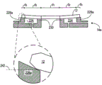
, with reference to Fig. 1 and 2, show the system 10 that forms relief pattern in substrate 12.Substrate 12 can have circular shape; Yet in another embodiment, substrate 12 can have any geometric configuration.In this example, substrate 12 can have inside radius r
1With external radius r
2Dish type, wherein, radius r
2Greater than radius r
1In addition, middle radius r
3Be formed on inside radius r
1With external radius r
2Between, wherein, middle radius r
3Be positioned at from inside radius r
1With external radius r
2Roughly equidistant place.
With reference to Fig. 1, substrate 12 can be connected to substrate chuck 14.As shown in the figure, substrate chuck 14 is vacuum type chucks, yet, substrate chuck 14 can be the chuck of any pattern, include but not limited to vacuum type, pin type, grooved or electromagnetic type, just as being entitled as the United States Patent (USP) 6 of " the high precision orientation alignment and the gas that are used for imprint lithography technique are controlled platform (High-Precision Orientation Alignment and Gap Control Stages for Imprint Lithography Processes) ", 873, described in 087 like that, this paper quotes this patent as a reference.Substrate 12 and substrate chuck 14 can be bearing on platform 16.In addition, substrate 12, substrate chuck 14 and platform 16 can be positioned on the base (not shown).Platform 16 can provide around the motion of the first and second axis, and the first and second axis are orthogonal, is x and y axle.With reference to Fig. 1,3 and 4, substrate chuck 14 comprises the first relative side 18 and the second side 20.Side surface or edge surface 22 extend between the first side 18 second sides 20.The first side 18 comprises first depression the 20, second depression the 22 and the 3rd depression 24, forms spaced each other the first support region 26, the second support region 28, the 3rd support region 30 and the 4th support region 32.The first support region 26 is around the second support region 28, the 3rd support region 30 and the 4th support region 32 and first depression the 20, second depression the 22 and the 3rd depression 24.The second support region 28 is around the 3rd support region 30 and the 4th support region 32 and the second depression the 22 and the 3rd depression 24.The 3rd support region 30 is around the 4th support region 32 and the 3rd depression 24.The 3rd depression 24 is around the 4th support region 32.In another embodiment, the first support region 26, the second support region 28, the 3rd support region 30 and the 4th support region 32 can be formed by compliant materials.The first support region 26, the second support region 28, the 3rd support region 30 and the 4th support region 32 can have circular shape; Yet in another embodiment, the first support region 26, the second support region 28, the 3rd support region 30 and the 4th support region 32 can comprise the geometric configuration of any requirement.
Being formed in substrate chuck 14 is path 34 and 36, yet substrate 12 can comprise any amount of path.Path 34 is put the first and the 3rd depression 20 and 24 and is communicated with side 18 fluids, yet, in another embodiment, should be understood that, path 34 can be put the first and the 3rd depression 20 and 24 and be communicated with any surfactant fluid of substrate chuck 14.Path 36 is put the second depression 22 and is communicated with side 18 fluids, yet, in another embodiment, should be understood that, path 36 can be put the second depression 22 and be communicated with any surfactant fluid of substrate chuck 14.In addition, it is desirable to, path 34 is convenient to put the first and the 3rd depression and 20 and 24 with the control pressurer system fluid such as pumping system 38, is communicated with, and path 36 is convenient to put second and is caved in and 22 with this control pressurer system fluid, be communicated with.
With reference to Fig. 1 and 5, patterning device 48 is spaced apart with substrate 12.Patterning device 48 comprises template 50, and this template has the table top 52 that extends towards substrate 12 from template, on it with patterned surfaces 54.In addition, table top 52 can be referred to as mould 52.In another embodiment, template 50 can there is no mould 52.Template 50 and/or mould 52 can be formed by such material, include but not limited to: the sapphire of fused silica, quartz, silicon, organic polymer, siloxane polymer, borosilicate glass, carbon fluorinated polymer, metal and sclerosis.As shown in the figure, patterned surfaces 54 comprises the feature that is limited by a plurality of isolated depressions 56 and projection 58.Yet in another embodiment, patterned surfaces 54 can be smooth and/or plane basically.Patterned surfaces 54 can limit master pattern, and this master pattern forms the basis of the pattern that will form in substrate 12.
With reference to Fig. 1,6 and 7, template 50 can be connected to template chuck 60, template chuck 60 can be any type of chuck, include but not limited to: vacuum type, pin type, grooved or electromagnetic type, just as being entitled as the United States Patent (USP) 6 of " the high precision orientation alignment and the gas that are used for imprint lithography technique are controlled platform ", described in 873,087 like that.Template chuck 60 comprises the first relative side 62 and the second side 64.Side surface or edge surface 66 extend between the first side 62 and the second side 64.The first side 62 comprises first depression the 68, second depression the 70 and the 3rd depression 72, forms spaced each other the first support region 74, the second support region 76 and the 3rd support region 78.The first support region 74 is around the second support region 70 and the 3rd support region 72 and first depression the 68, second depression the 70 and the 3rd depression 72.The second support region 76 is around the 3rd support region 78 and the second depression the 70 and the 3rd depression 72.The 3rd support region 78 is around the 3rd depression 72.In another embodiment, the first support region 74, the second support region 76 and the 3rd support region 78 can be formed by compliant materials.The first support region 74, the second support region 76 and the 3rd support region 78 can have circular shape; Yet in another embodiment, the first support region 74, the second support region 76 and the 3rd support region 78 can comprise the geometric configuration of any requirement.
Being formed in template chuck 60 is path 80 and 82, yet template chuck 60 can comprise any amount of path.Path 80 is put the first and the 3rd depression 68 and 72 and is communicated with the second side 64 fluids, yet, in another embodiment, should be understood that, path 80 can be put the first and the 3rd depression 68 and 72 and be communicated with any surfactant fluid of template chuck 60.Path 82 is put the second depression 70 and is communicated with the second side 64 fluids, yet, in another embodiment, should be understood that, path 80 can be put the second depression 70 and be communicated with any surfactant fluid of template chuck 60.In addition, it is desirable to, path 80 is convenient to put the first and the 3rd depression and 68 and 72 with the control pressurer system fluid such as pumping system 84, is communicated with, and path 82 is convenient to put second and is caved in and 70 with this control pressurer system fluid, be communicated with.
With reference to Fig. 1, system 10 also comprises fuid distribution system 98.Fuid distribution system 98 can be communicated with substrate 12 fluids, so that precipitation polymers formed material 100 thereon.Fuid distribution system 98 can comprise a plurality of allocation units therein.Should be understood that, polymkeric substance formed material 100 can use any known technology to precipitate, for example, drop precipitation, spin coated, dip coating, chemical vaporization precipitation (CVD), physical evaporation precipitation (PVD), thin film deposition, thick film precipitation etc.Typically, polymkeric substance formed material 100 can be deposited in substrate 12 before the volume that requires is formed on 12 of mould 52 and substrates.Yet polymkeric substance formed material 100 also can be filled this volume after obtaining desirable volume.As shown in Figure 8, polymkeric substance formed material 100 can be deposited in substrate 12 as a plurality of isolated drops 102, forms matrix array 104.In one example, each in drop 102 is dripped and can be had the unit volume that is approximately 1-10 micromicro liter (pico-liter).Drop 102 can any two-dimensional arrangement mode be arranged in substrate 12.
With reference to Fig. 1 and 9, system 10 also comprises that along path 110 are connected to energy 108 sources 106 of DIRECT ENERGY 108.Imprint head 97 and platform 16 are configured to respectively mould 52 and substrate 12 are arranged to overlapping and are arranged in path 110.No matter imprint head 97, platform 16 or they both change distance between mould 52 and substrate 12, to limit betwixt the volume of ideal of by polymkeric substance formed material 100, being filled.After with polymkeric substance formed material 100, filling volume of ideal, source 106 produce powers 108, for example, the ultraviolet radiation in broadband, it causes polymkeric substance formed material 100 to solidify and/or is crosslinked, accords with the surface 112 of substrate 12 and the shape of patterned surfaces 54, and form patterned layer 114 in substrate 12.Patterned layer 114 can comprise residual layer 116 and a plurality of feature that is shown as projection 118 and depression 120.The control of this process is regulated by processor 122, and this processor 122 carries out data with platform 16, pumping system 38 and 84, imprint head 97, fuid distribution system 98 and source 106 and is communicated with, the enterprising line operate of the computer-readable program in being stored in storer 124.
With reference to Fig. 1, system 10 also comprises the pin 126 that is connected to platform 16.Pin 126 can be around the 3rd axis translation that is orthogonal to the first and second axis, that is, and and along the translation of z axis.Consequently, pin 126 can contact mould 52 and change its shape, and this will be described below.Pin 126 can be power or the displacement actuator of any type well known in the art, especially comprises pneumatic, piezoelectricity, magnetostrictive, linear and voice coil.In another embodiment, pin 126 can be the air slide of high-resolution pressure governor and cleaning series, and it is with the centrepin that comprises vacuum source, the interface that this vacuum source can emptying patterning device 48 and the atmosphere between substrate 12.
With reference to Fig. 1,8 and 9, as mentioned above, the distance variable between mould 52 and substrate 12, to form betwixt the volume of ideal of by polymkeric substance formed material 100, being filled.In addition, after solidifying, polymkeric substance formed material 100 accords with the surface 112 of substrate 12 and the shape of patterned surfaces 54, forms patterned layer 114 in substrate 12.For this reason, be formed in the volume 128 between the drop 102 of matrix array 104 and have gas, drop 102 in matrix array 104 is dispersed in substrate 12, can avoid having gas and/or air bag (if undebarred words) between substrate 12 and mould 52 He in patterned layer 114.Gas and/or air bag can be such gas, include but not limited to: air, nitrogen, carbon dioxide and helium.Between substrate 12 and mould 52 and the distortion that especially causes the interior formation pattern characteristics of patterned layer 114 of the gas in patterned layer 114 and/or air bag, the low fidelity of the interior formation feature of patterned layer 114, and across the off-gauge of the residual layer 116 of patterned layer 114, all these is undesirable.For this reason, below description is made between substrate 12 and mould 52 and patterned layer 114 in have gas and/or the air bag method and system for minimum (if undebarred words).
With reference to Fig. 1 and 10, in the first embodiment, the method for gas between expulsion substrate 12 and mould 52 shown in figure.Specifically, at step 200 place, as mentioned above, polymkeric substance formed material 100 can be positioned in substrate 12 with methods such as drop precipitation, spin coated, dip coating, chemical vaporization precipitation (CVD), physical evaporation precipitation (PVD), thin film deposition, thick film precipitations.In another embodiment, polymkeric substance formed material 100 can be positioned on mould 52.
, with reference to Fig. 6,7,10 and 11,, at step 202 place, can change the shape of patterning device 48.Specifically, the shape of patterning device 48 can change over the middle radius r that makes substrate 12
3Place is formed on and is formed on distance between mould 52 and substrate 12 apart from d1 (as shown in Figure 2) less than mould 52 remainder places between mould 52 and substrate 12.In one example,, less than distance d2, be formed on the edge of mould 52 apart from d1 apart from d2.In another embodiment, can be formed on any ideal position place of mould 52 apart from d1.The shape of patterning device 48 can change by the pressure of controlling in the first chamber 68 and the 3rd chamber 72.Specifically, as mentioned above, operating pumps system 84 is controlled the pressure in the first chamber 68 and the 3rd chamber 72.For this reason, pumping system 84 can be by path 80 in the first chamber 68 and the interior formation vacuum of the 3rd chamber 72, makes the part 86a of template 50 and 86c can be away from substrate 12 crooked and towards template chuck 60 bendings.Away from substrate 12 bendings, the part 86b of template 50 is towards substrate 12 and away from template chuck 60 bendings due to the part 86a of template 50 and 86c.
With reference to Figure 10,12 and 13, at step 204 place, as described above in reference to Figure 1, be no matter imprint head 97 shown in Figure 1, platform 16 or they both can change as shown in Figure 1 apart from d1, so that the subdivision of the part of mould 52 contact drop 102.As shown in the figure, before all the other drops of the remainder of mould 52 contact drop 102, the middle radius r of mould 52 and substrate 12 as shown in Figure 2
3The subdivision of overlapping part contact drop 102.Yet in another embodiment, any part of mould 52 can contact drop 102 before the remainder contact of mould 52.For this reason, as shown in the figure, mould 52 side by side contacts the middle radius r with substrate 12 basically
3All overlapping drops 102, as shown in Figure 2.This causes drop 102 to scatter and form the liquid sheet of adjoining 130 of polymkeric substance formed material 100.The edge 132 of liquid sheet 130 forms liquid-gas interface 134, and the function of this interface is to push away the edge 136 of the interior gas of volume 128 towards substrate 12.Volume 128 between drop 102 forms gas passage, can push gas to edge 136 by this gas passage.Its result, the liquid that is associated with gas passage-gas interface 134 reduces, if undebarred words, gas residue is in liquid sheet 130.
With reference to Fig. 7,10 and 14,, at step 206 place, can change the shape of patterning device 48, make the volume of ideal that is formed between mould 52 and substrate 12 can be aggregated materialization material 100 and fill, as described above in reference to Figure 1.Specifically, the shape of patterning device 48 can change in the following manner: control the pressure in the first and the 3rd chamber 88 and 96, and acted on the combination of the power on patterning device 48 due to polymkeric substance formed material 100 with contacting of mould 52 by imprint head 97 (as shown in Figure 1) and/or platform 16.Specifically, as mentioned above, operating pumps system 84 is controlled the pressure in the first and the 3rd chamber 88 and 96.For this reason, pumping system 84 reduces the vacuum size of the first and the 3rd chamber 88 and 96 interior formation by path 80, makes the middle radius r with substrate 12 around as shown in Figure 2
3The relevant polymkeric substance formed material 100 of the collection of subgroup thereafter of drop 100 scatter and become and include in the fluid sheet 130 that adjoins, as shown in figure 14.The shape of patterning device 48 continues to change, and mould 52 contact with all the other drops 102 subsequently, makes polymkeric substance formed material associated with it 100 distributions and becomes and include in the fluid sheet 130 that adjoins, as shown in figure 15.Can see, interface 134 136 moves towards edge, thereby has the without hindrance path of gas by wherein advancing that is used in all the other volumes 128, as shown in Figure 8.This allows the interior gas of volume 128 and edge 136 Face to face from discharging between mould 52 and substrate 12.Like this, if undebarred words make to remain between substrate 12 and mould 52 to minimize with patterned layer 114 interior gas and/or air bags, as shown in Figure 9.In another embodiment, the shape of patterning device 48 can be with the reducing and change simultaneously of distance d1, as above described with reference to Figure 11., with reference to Fig. 7 and 12, in also having an embodiment,, for the ease of changing the shape of patterning device 48, can control the pressure in the second chamber 92.Specifically, as mentioned above, operating pumps system 84 is controlled the pressure in the second chamber 92.For this reason, pumping system 84 can pass through path 82 mineralization pressures in the second chamber 92, makes the part 86c of template 50 can be towards substrate 12 crooked and away from template chuck 60 bendings.In addition, as mentioned above, can be with the first and the 3rd chamber 88 and 96 interior formation vacuum and side by side at the second interior mineralization pressure of chamber 92.
With reference to Fig. 1 and 10, at step 208 place, as described above in reference to Figure 1, polymkeric substance formed material 100 is then curable and/or crosslinked, forms patterned layer 114, as shown in Figure 9.Thereafter, at step 210 place, mould 52 can separate with patterned layer 114, as shown in Figure 9.
With reference to another embodiment of the present invention shown in Fig. 1 and 16, figure.Specifically,, at step 300 place, be similar to above describedly like that with reference to step 200 shown in Figure 10, polymkeric substance formed material 100 can be positioned on substrate 12 or mould 52.
With reference to Fig. 3,4,16 and 17,, at step 302 place, be similar to above describedly like that with reference to step 202 shown in Figure 10, the shape of patterning device 48 can change.In addition, along with the change of patterning device 48 shapes, the shape of substrate 12 can change simultaneously.Specifically, the shape of substrate 12 can change by the pressure of controlling in the first and the 3rd chamber 42 and 46.Specifically, as mentioned above, operating pumps system 38 is controlled the pressure in the first and the 3rd chamber 42 and 46.For this reason, pumping system 38 can be by path 36 in the first and the 3rd chamber 42 and 46 interior formation vacuum, make the part 40a of substrate 12 and 40c can be away from substrate chuck 14 crooked and towards mould 52 bendings, as shown in figure 17., away from substrate chuck 14 bendings, make the part 40b of substrate 12 towards mould 52 with away from substrate chuck 14 bendings due to the part 40a of substrate 12 and 40c.With reference to Figure 11,13 and 16, at step 304 place, be similar to above describedly like that with reference to step 204 shown in Figure 10, imprint head 97, platform 16 or they both can change apart from d1, as shown in figure 11, make the middle radius r of part contact with the substrate 12 of mould 52
3The subdivision of overlapping drop 102, as shown in Figure 2, side by side produce thereafter the contiguous liquid sheet 130 of polymkeric substance formed material 100.
With reference to Fig. 4,12 and 16,, at step 306 place, be similar to above describedly like that with reference to step 206 shown in Figure 10, the shape of patterning device 48 can change, and the volume of ideal usable polymers formed material 100 that forms between mould 52 and substrate 12 is filled.In addition, along with the change of patterning device 48 shapes, the shape of substrate 12 can change simultaneously.Specifically, as mentioned above, operating pumps system 38 is controlled the pressure in the first chamber 42 and the 3rd chamber 46.For this reason, pumping system 38 reduces the vacuum size of the first and the 3rd chamber 42 and 46 interior formation by path 36, change the shape of patterning device 48 simultaneously in step 204 shown in Figure 10 as described above, makes and middle radius r around substrate 12
3The polymkeric substance formed material 100 (as shown in Figure 2) that is associated of drop 102 scatter and become and include in the fluid sheet 130 that adjoins, as shown in figure 14.The shape of substrate 12 also can further change in company with the change of shape of patterning device 48, make mould 52 contact with all the other drops 102 subsequently, become and be incorporated in adjacent fluids sheet 130 thereby polymkeric substance formed material associated with it 100 scatters, as shown in figure 15.Gas in volume 128 as shown in Figure 8 can by with above with reference to the described roughly the same method of step 206 shown in Figure 10, and edge 136 is Face to face from discharging between mould 52 and substrate 12.
, with reference to Fig. 3 and 4,, in order further to be convenient to change the shape of substrate 12, can control the pressure in the second chamber 44.Specifically, as mentioned above, operating pumps system 38 is controlled the pressure in the second chamber 44.For this reason, pumping system 38 can pass through path 34 mineralization pressures in the second chamber 44, makes a part of 40b of substrate 50 can be towards mould 52 crooked and away from substrate chuck 14 bendings.In addition, as mentioned above, can be with the first and the 3rd chamber 42 and 46 interior formation vacuum and side by side at the second interior mineralization pressure of chamber 44.
With reference to Fig. 1 and 10, at step 308 place, as described above in reference to Figure 1, polymkeric substance formed material 100 is then curable and/or crosslinked, forms patterned layer 114, as shown in Figure 9.Thereafter, at step 310 place, mould 52 can separate with patterned layer 114, as shown in Figure 9.
, with reference to Fig. 6 and 18, in another embodiment,, for ease of changing the shape of patterning device 48, can adopt pin 126.Specifically, pin 126 can apply power to patterning device 48, in this example, is to act on the third part 86c of template 50.Its result, patterning device 48 can comprise above-mentioned desirable changes shape, and can use in above-mentioned any method.Also can be convenient to separating of mould 52 and substrate 12 with pin 126, just as above respectively with reference to the step 208 as shown in Figure 10 and 16 and 308 described.In addition, after patterned layer 114 formed, as shown in Figure 9, pin 126 can be away from patterning device 48 translations, and make patterning device 48 basically be flat.Pin 126 can with processor 122 UNICOMs can utilize the feedback of power to carry out the size of deterministic force so that sell 126.
, with reference to Figure 19,, in order further to be convenient to separating of mould 52 and substrate 12, can introduce gas 148 between substrate 12 and mould 52 by pin 126.Specifically, pin 126 can comprise the path 150 with the hole 152 that is communicated with the control pressurer system fluid, control pressurer system such as pumping system 38.In another embodiment, pin 126 can comprise any amount of hole.Hole 152 can be positioned to gas 148 is incorporated between mould 52 and substrate 12.148 pairs of moulds 52 of gas and substrate 12 apply power, along promoting mould 52 away from the direction of substrate 12 and away from the direction of mould 52, promoting substrate 12.As shown in the figure, when pin 126 close template 50, gas 148 can be incorporated between mould 52 and substrate 12; Yet, in another embodiment, can when pin 126 is in any position, gas 148 be introduced between mould 52 and substrate 12.
Figure 20 illustrates another embodiment of substrate chuck 14a shown in Figure 1, and it can provide single ripple of substrate 12 crooked.At single wave pressure India and China, the interior diameter d of substrate 12
1Can make the droop error between susceptibility, template 18 and the substrate 12 of chuck 14 heterogeneities (for example, flatness) and/or the axial error between template 18 and substrate 12 are reduced to minimum.Interior diameter d due to substrate 12
1Can lay in as non-imprinting area, it is minimum that impression defect and/or detachment defects all can be reduced to.In addition, chuck 14a can make the overall diameter d of substrate 12
3And the contact between chuck 14a reduces to minimum, with reduce injection defect.
As shown in figure 20, support region 228 can comprise height h
1, its height higher than support region 230 h
2The height h of support region 228
1Can have the height h than support region 230
2High numerical value, to obtain single ripple distortion in the process in impression substrate 12.Single ripple distortion usually can be described as the shape of single ripple, and wherein, substrate 12 presents recessed bending, so that the surface 229 of substrate 12 can be tangential on support region 230 and/or support region 228 basically.For example, the height h of support region 228
1Can have the height h than support region 230
2The numerical value of about 80 microns.In addition, the height h of support region 228
1, support region 230 height h
2And/or the height h of support region 228
1Height h with support region 230
2Between difference can be based on the thickness t of substrate 12
1And/or the material of substrate 12 and determining.For example, for thickness t
1Be approximately the substrate 12 of the fused silica of 635 microns, the height h of support region 228
1Height h with support region 230
2Between difference can be approximately 100 microns.
The overall diameter d of substrate 12
3Can be usually the first burble point, will require that maximum hold facility is arranged in the process of the patterned layer 46 that impresses separating template 18 and stand thereafter like this, just as described with reference to Fig. 1 and 2.By increasing the height h of support region 228
1, the vacuum power that is provided by chuck 14 diameter d outward of can setovering
3The biasing of vacuum power can reduce required confining force and/or reduce required separating force in template 18 and patterned layer 46 detachment processes.
, with reference to Figure 21 A-21C, in one embodiment, add definite feature described here to or substitute feature (for example, the thickness t that this is determined
1, substrate 12 material and/or suchlike feature), the height h of support region 228
1Can be determined according to the predetermined pressure level that control pressurer system is applied on depression 224 and/or 226.For example, the height h of support region 228
1Can measured stress level, this pressure provides substrate 12 single ripple as shown in figure 20 when applying.In moulding process, because substrate 12 is single ripple, as described herein, the interior diameter d of substrate 12
2Can be basically recessed shape.
Stress level can be suitable for the height h according to support region 228
1Single ripple distortion of substrate 12 is provided.For example, Figure 21 A shows and stands the approximately substrate 12 of 0kPa.Substrate 12 approximately can represent suitable flatness under 0kPa.In addition, but substrate 12 and support region 230 distance of separation d.For example, substrate 12 and support region 230 can separate approximately 100 microns.With reference to Figure 21 B, path 232 and 234 can provide depression 224 approximately-5kPa and with the crooked substrate 12 of the shape of single ripple roughly, wherein, substrate 12 presents recessed bending, so that the surface 229 of substrate 12 can be tangential on support region 230 basically.Approximate-during 80kPa, although the part of substrate 12 can still be tangential on support region 230 basically, substrate 12 presents the double wave shape, in depression 224 a plurality of recessed bendings of interior formation.
With reference to Figure 22 A and 22B, in one embodiment, chuck 14 can provide the substrate 12 of monophasic waveform state in moulding process, and the while is diameter d outside
3Locate to reduce as far as possible and/or eliminate defect.For example, Figure 22 A illustrates the one exemplary embodiment of chuck 14a, and wherein, chuck 14a comprises the boss 228a of taper.Cone boss 228a is diameter d outside
3Place provides the minimal-contact between chuck 14 and substrate 12.Contact also minimizes and can make overall diameter d
3The defect at place is minimum.Cone boss 228a can comprise the height h greater than support region 230
2Height h
1In addition, the tapered edge 240 of cone boss 228a can be set the angle (for example, being approximately 2-5 °) with respect to axis 242.This angle can be suitable for making cone boss 228a to have contact or the not contact minimum with the edge 244 (that is, flat zone) of substrate 12, as shown in Figure 22 A.
Figure 22 B illustrates another one exemplary embodiment of chuck 14a, and wherein, chuck 14a comprises substantially flat boss 228b.The location of the substrate 12 of monophasic waveform shape can provide from generally flat boss 228b distance g
1The overall diameter d of the substrate 12 at place
3
With reference to Figure 23, in one embodiment, template chuck 28a can provide the patterned surfaces 22 of template 18, to accord with the monophasic waveform shape of substrate 12 in impression and/or detachment process.Template chuck 28a can comprise path 254, and this path 254 is suitable for providing vacuum and/or the pressure that affects template 18 shapes.For example, path 254a can provide and can keep the outer peripheral vacuum of template 18, so that template 18 outward flanges are towards chuck 28 bendings.Path 254b can provide vacuum and/or pressure, makes template 18De center towards substrate 12 bendings.Template 18De center can contact the substrate 12 that accords with the monophasic waveform shape.For example, template 18De center can contact the interior diameter d of substrate 12
1, make the overall diameter d of the fluid motion of polymkeric substance formed material 34 towards substrate 12
3Flow.In addition, in detachment process, last separation can occur in the center of template 18, makes the interior diameter d of substrate 12
1Have the substrate 12 of monophasic waveform shape and accord with the shape of template 18.
With reference to Figure 24 A-D, in another embodiment, template chuck 28b can be at impression and/or the patterned surfaces 22 of the template 18 of double wave form is provided in separating the process of the substrate 12 with monophasic waveform shape.
With reference to Figure 24 A, the path 560a-560c of template chuck 28b can provide vacuum and/or pressure, with the template 18 that the double wave form is provided.For example, path 560b can provide pressure, and path 560a and 560c can provide vacuum in the chamber that is formed by boss 562a-562f (for example, three or more chambers).The template 18 that pressure in chamber and/or vacuum can provide the double wave form so that template 18 with the overlapping part of path 560b towards substrate 12 bendings, and template 18 with path 560a and the overlapping part of 560c can be away from substrate 12 bendings.Template 18 can first contact substrate 12 with the overlapping part of path 560b.Should be noted that, can use additional path 560 and/or chamber.As shown in Figure 24 B, can reduce vacuum and/or reduce pressure, so that the remainder of template 18 contact substrates 12.Especially, the part overlapping with path 560c of template 18 (for example, overlapping with the interior diameter of substrate 12) can contact substrate 12 finally.Like this, the gas between template 18 and substrate 12 can be emptying at substrate 12 interior diameter places.
In moulding process, usually the surface of substrate 12 can be arranged on substrate chuck 14 basically in the shape of fine control, to avoid the Fluid Anomalies ground distribution of any part.Yet the local surfaces cohesive force of covering between the patterned surfaces 46 in cover 20 and substrate 12 can be over the bed knife from substrate chuck 14.This can cause substrate 12 in the local bending of imprinting area boundary.So local bending can cause vacuum to keep the loss of pressure, like this, can cause separating unsuccessfully.
, with reference to Figure 25-27,, in addition to or in lieu substrate chuck 14, can provide constraint to substrate 12 by keeping system 660.In general, keeping system 660 can engage substrate 12, in patterned layer as described herein and template detachment process, by making F firmly, can provide constraint to substrate 12.In one embodiment, keeping system 660 is around substrate 12.In another embodiment, a plurality of keeping systems 660 can be placed around substrate 12 on strategy ground, to provide constraint to substrate 12 in template 18 and substrate 12 detachment processes.
Keeping system 660 can comprise contact head 668 and body 669.Contact head 668 can provide power F to come at the bottom of bound base 12.Contact head 668 considers it can is static or adjustable according to design.
In case with substrate 12, contact, contact head 668 just can basad 12 provides power F, is used for substrate 12 is tied to substrate chuck 14.For example, the chamfered edge 664 that contact head 668 can basad 12 provides power F, as shown in figure 27,, with in detachment process as described herein, basically substrate 12 is tied to substrate chuck 14.
Keeping system 660 also can comprise base 666.In general, body 669 can be attached to base 666 with adjusting, so that the radial motion of body 669 around x and y axle to be provided.Body 669 can provide distance between substrate 12 and contact head 668 around the radial motion of base 666, is used for loading and unloading substrate 12.For example, as shown in figure 26, in primary importance, body 669 can be positioned on base 666, so that contact head 668 can contact with substrate 12.As shown in figure 27, in the second place, body 669 can provide contact head 668 to be positioned at setpoint distance D place apart from substrate 12 around the radial motion of base 666.In this position, substrate 12 is not hindered by contact head 668 can, therefore can unload from system 10 as shown in Figure 1.Body 669 usually is not more than substrate 12 loadings and unloads required scope around the range of movement of base 666.For example, body 669 can be at 50 microns to the magnitude of 1mm around the range of movement of base 666.Perhaps, body 669 considers to exceed general loading and the required requirement of unloading substrate 12 around the motion of base 666 according to design.
In detachment process as described herein, when body contact substrate 12, base 666 can provide additional force F to body 669
cBe used at the bottom of bound base 12.In an example, body 669 adjustable grounds are attached to base 666, to provide around the constraining force F of z axle
cFor example, contact head 668 can be connected to base 666 by vacuum prestrain air bearing, magnetic prestrain air bearing and/or suchlike bearing.
Figure 28 illustrates in template 18 and substrate 12 detachment processes and is used at the bottom of bound base the process flow diagram 680 of 12 exemplary method.In step 682, substrate 12 can be loaded into system 10.In step 684, contact head 668 can be placed to contact substrate 12.For example, the surface 670 of contact head 668 can contact the chamfered edge 664 of substrate 12.In step 686, contact head 668 can provide at the bottom of bound base 12 power F.In step 688, base 666 can provide to retrain the power Fc of body 669.In step 690, system 10 can be carried out moulding process.In step 692, contact head can separate with substrate 12 by the radial motion of body 669 around base 666.In step 690, substrate 12 can unload from system 10.
Claims (14)
1. device that is used for support base comprises:
Be suitable for the vacuum chuck of support base, described vacuum chuck has:
Be suitable for supporting the outer lug boss of the overall diameter of described substrate, described outer lug boss has the first height; And
Spaced apart and be suitable for supporting the inner convex platform of the interior diameter of described substrate with described outer lug boss, described inner convex platform has the second height, and this second height is less than the first height of described outer lug boss;
Wherein, determine described the first height and described the second height so that the substrate of monophasic waveform state to be provided, and the biasing of vacuum power towards the overall diameter of described substrate is provided.
2. device as claimed in claim 1, is characterized in that, also comprises the template chuck that is suitable for supporting the imprint lithography template, and described template chuck has boss and the path of a plurality of formation chambers.
3. device as claimed in claim 2, is characterized in that, at least one described chamber provides pressure to described imprint lithography template, and at least one described chamber provides vacuum to described imprint lithography template.
4. device as claimed in claim 3, is characterized in that, described chamber is suitable for providing the imprint lithography template of monophasic waveform state.
5. device as claimed in claim 3, is characterized in that, described chamber is suitable for providing the imprint lithography template of double wave form.
6. device as described in any one in claim 1 to 5, is characterized in that, outer lug boss is taper.
7. device as claimed in claim 1, is characterized in that, also comprises:
Keeping system, described keeping system comprises:
Body; And
Contact head, described contact head is connected to adjustably described body and is suitable for providing the power that described substrate is tied to described vacuum chuck, described contact head has at least one surface, this surface is positioned to respect to described body at angle, so that align with the chamfered edge of described substrate in described surface.
8. device as claimed in claim 7, is characterized in that, also comprises that adjustable ground is attached to the base on described body, and described base provides the radial motion of body around one or more axis.
9. device as claimed in claim 7, is characterized in that, described body can be at 50 microns between 1mm around the scope of described base motion.
10. imprint lithography method comprises:
Substrate is fixed on device as claimed in claim 1;
Template is fixed on template chuck, and described template chuck is suitable for providing the template of double wave form, and described double wave form has the part towards described substrate bending of described template and the part away from described substrate bending of described template;
Make the contact of the part towards described substrate bending of described template be positioned at described suprabasil polymkeric substance formed material; And
Make the described substrate of remainder contact of described template.
11. method as claimed in claim 10, is characterized in that, also comprises the interior diameter Exhaust Gas by described substrate.
12. method as described in claim 10 or 11, is characterized in that, also comprises the polymkeric substance formed material that forms patterned layer is solidified; And make described template and be positioned at described suprabasil patterned layer and separate.
13. method as claimed in claim 12, is characterized in that, the last contact point between described template and described patterned layer and the interior diameter of described substrate are overlapping.
14. method as described in claim 10 or 11, is characterized in that, described outer lug boss provides and the contacting of the overall diameter minimum of described substrate.
Applications Claiming Priority (7)
| Application Number | Priority Date | Filing Date | Title |
|---|---|---|---|
| US10772908P | 2008-10-23 | 2008-10-23 | |
| US61/107,729 | 2008-10-23 | ||
| US10864008P | 2008-10-27 | 2008-10-27 | |
| US61/108,640 | 2008-10-27 | ||
| US12/582,091 | 2009-10-20 | ||
| US12/582,091 US8215946B2 (en) | 2006-05-18 | 2009-10-20 | Imprint lithography system and method |
| PCT/US2009/005721 WO2010047788A2 (en) | 2008-10-23 | 2009-10-21 | Imprint lithography system and method |
Publications (2)
| Publication Number | Publication Date |
|---|---|
| CN102203672A CN102203672A (en) | 2011-09-28 |
| CN102203672B true CN102203672B (en) | 2013-11-13 |
Family
ID=42036819
Family Applications (1)
| Application Number | Title | Priority Date | Filing Date |
|---|---|---|---|
| CN2009801427660A Expired - Fee Related CN102203672B (en) | 2008-10-23 | 2009-10-21 | Imprint lithography system and method |
Country Status (6)
| Country | Link |
|---|---|
| US (1) | US8215946B2 (en) |
| JP (2) | JP5289577B2 (en) |
| CN (1) | CN102203672B (en) |
| MY (1) | MY165977A (en) |
| SG (1) | SG195597A1 (en) |
| WO (1) | WO2010047788A2 (en) |
Cited By (1)
| Publication number | Priority date | Publication date | Assignee | Title |
|---|---|---|---|---|
| US11846890B2 (en) | 2016-10-20 | 2023-12-19 | Molecular Imprints, Inc. | Positioning substrates in imprint lithography processes |
Families Citing this family (33)
| Publication number | Priority date | Publication date | Assignee | Title |
|---|---|---|---|---|
| JP4340086B2 (en) * | 2003-03-20 | 2009-10-07 | 株式会社日立製作所 | Nanoprinting stamper and fine structure transfer method |
| NL2002672C2 (en) * | 2009-03-26 | 2010-09-28 | Stork Titan Bv | MASS DIVIDING DEVICE AND MOLDING DEVICE CONTAINING SUCH A MASS DIVIDING DEVICE. |
| US9164375B2 (en) * | 2009-06-19 | 2015-10-20 | Canon Nanotechnologies, Inc. | Dual zone template chuck |
| JP2011071500A (en) * | 2009-08-31 | 2011-04-07 | Fujifilm Corp | Pattern transfer apparatus and pattern forming method |
| JP5395756B2 (en) * | 2010-07-07 | 2014-01-22 | 株式会社東芝 | Imprint template manufacturing method and pattern forming method |
| JP2013538447A (en) * | 2010-08-05 | 2013-10-10 | エーエスエムエル ネザーランズ ビー.ブイ. | Imprint lithography |
| US8741199B2 (en) * | 2010-12-22 | 2014-06-03 | Qingdao Technological University | Method and device for full wafer nanoimprint lithography |
| NL2006841C2 (en) * | 2011-05-24 | 2012-11-27 | Marel Townsend Further Proc Bv | FORMATION DEVICE, AND METHOD FOR FORMING A FOOD PRODUCT. |
| JP5492162B2 (en) * | 2011-09-01 | 2014-05-14 | 株式会社日立ハイテクノロジーズ | Microstructure transfer device |
| JP2013064836A (en) * | 2011-09-16 | 2013-04-11 | Olympus Corp | Manufacturing method of mold for forming fine structure and optical element |
| KR20130085759A (en) | 2012-01-20 | 2013-07-30 | 삼성전자주식회사 | Stamp and method of fabricating stamp and imprinting method using the same |
| JP6304934B2 (en) * | 2012-05-08 | 2018-04-04 | キヤノン株式会社 | Imprint apparatus and article manufacturing method |
| JP6000656B2 (en) * | 2012-05-30 | 2016-10-05 | 株式会社日立ハイテクノロジーズ | Resin stamper manufacturing apparatus and resin stamper manufacturing method |
| DE102012111114B4 (en) * | 2012-11-19 | 2018-10-04 | Ev Group E. Thallner Gmbh | Semiconductor processing apparatus and method |
| JP6412317B2 (en) | 2013-04-24 | 2018-10-24 | キヤノン株式会社 | Imprint method, imprint apparatus, and article manufacturing method |
| JP6497839B2 (en) * | 2013-11-07 | 2019-04-10 | キヤノン株式会社 | Imprint apparatus and article manufacturing method |
| EP3066524A1 (en) | 2013-11-08 | 2016-09-14 | Canon Nanotechnologies, Inc. | Low contact imprint lithography template chuck system for improved overlay correction |
| JP6333031B2 (en) * | 2014-04-09 | 2018-05-30 | キヤノン株式会社 | Imprint apparatus and article manufacturing method |
| KR102394754B1 (en) * | 2014-04-22 | 2022-05-04 | 에베 그룹 에. 탈너 게엠베하 | Method and device for embossing a nanostructure |
| US10620532B2 (en) * | 2014-11-11 | 2020-04-14 | Canon Kabushiki Kaisha | Imprint method, imprint apparatus, mold, and article manufacturing method |
| JP6441181B2 (en) * | 2015-08-04 | 2018-12-19 | 東芝メモリ株式会社 | Imprint template, method for manufacturing the same, and method for manufacturing a semiconductor device |
| JP6774178B2 (en) * | 2015-11-16 | 2020-10-21 | キヤノン株式会社 | Equipment for processing substrates and manufacturing methods for articles |
| US11104057B2 (en) * | 2015-12-11 | 2021-08-31 | Canon Kabushiki Kaisha | Imprint apparatus and method of imprinting a partial field |
| TWI672212B (en) * | 2016-08-25 | 2019-09-21 | 國立成功大學 | Nano imprinting assembly and imprinting method thereof |
| KR102326522B1 (en) | 2016-10-18 | 2021-11-12 | 몰레큘러 임프린츠 인코퍼레이티드 | Microlithographic fabrication of structures |
| JP6762853B2 (en) * | 2016-11-11 | 2020-09-30 | キヤノン株式会社 | Equipment, methods, and article manufacturing methods |
| US11454883B2 (en) | 2016-11-14 | 2022-09-27 | Canon Kabushiki Kaisha | Template replication |
| US10969680B2 (en) * | 2016-11-30 | 2021-04-06 | Canon Kabushiki Kaisha | System and method for adjusting a position of a template |
| JP6940944B2 (en) | 2016-12-06 | 2021-09-29 | キヤノン株式会社 | Imprint device and article manufacturing method |
| TWI666128B (en) * | 2018-07-24 | 2019-07-21 | 奇景光電股份有限公司 | Measuring fixture |
| US11198235B2 (en) * | 2018-08-09 | 2021-12-14 | Canon Kabushiki Kaisha | Flexible mask modulation for controlling atmosphere between mask and substrate and methods of using the same |
| JP7410616B2 (en) | 2019-09-24 | 2024-01-10 | キヤノン株式会社 | Flattening device, article manufacturing method, flattening method, and imprint device |
| JP7418127B2 (en) | 2020-03-24 | 2024-01-19 | キヤノン株式会社 | Flattening device, flattening method, and article manufacturing method |
Citations (6)
| Publication number | Priority date | Publication date | Assignee | Title |
|---|---|---|---|---|
| US4395211A (en) * | 1979-08-10 | 1983-07-26 | U.S. Philips Corporation | Method and device for manufacturing a plastic record carrier |
| WO1997005608A1 (en) * | 1995-07-27 | 1997-02-13 | Minnesota Mining And Manufacturing Company | Method and apparatus for making an optical information record |
| EP1072954A2 (en) * | 1999-07-28 | 2001-01-31 | Lucent Technologies Inc. | Lithographic process for device fabrication |
| WO2007067469A2 (en) * | 2005-12-08 | 2007-06-14 | Molecular Imprints, Inc. | Method for expelling gas positioned between a substrate and a mold |
| WO2007126767A2 (en) * | 2006-04-03 | 2007-11-08 | Molecular Imprints, Inc. | Chucking system comprising an array of fluid chambers |
| WO2007136832A2 (en) * | 2006-05-18 | 2007-11-29 | Molecular Imprints, Inc. | Method for expelling gas positioned between a substrate and a mold |
Family Cites Families (197)
| Publication number | Priority date | Publication date | Assignee | Title |
|---|---|---|---|---|
| BE687248A (en) | 1966-09-22 | 1967-03-22 | ||
| US3997447A (en) | 1974-06-07 | 1976-12-14 | Composite Sciences, Inc. | Fluid processing apparatus |
| IT1068535B (en) | 1975-11-03 | 1985-03-21 | Ibm | APPARATUS AND GRAPHIC ELECTROLYTE PROCESS |
| NL177721B (en) | 1977-03-14 | 1985-06-03 | Philips Nv | METHOD FOR MANUFACTURING A PLASTIC INFORMATION CARRIER WITH LAYERED STRUCTURE AND AN APPARATUS FOR CARRYING OUT THE METHOD |
| NL7710555A (en) | 1977-09-28 | 1979-03-30 | Philips Nv | METHOD AND DEVICE FOR MANUFACTURING INFORMATION CONTAINING PLATES. |
| US4279628A (en) | 1979-12-31 | 1981-07-21 | Energy Synergistics, Inc. | Apparatus for drying a natural gas stream |
| DE8007086U1 (en) | 1980-03-14 | 1982-03-18 | Multivac Sepp Haggenmüller KG, 8941 Wolfertschwenden | DEVICE FOR MOLDING CONTAINERS FROM A FILM |
| JPS57204547A (en) | 1981-06-12 | 1982-12-15 | Hitachi Ltd | Exposing method |
| JPS59107723U (en) * | 1982-12-29 | 1984-07-20 | 富士通株式会社 | disk fixing device |
| US4551192A (en) | 1983-06-30 | 1985-11-05 | International Business Machines Corporation | Electrostatic or vacuum pinchuck formed with microcircuit lithography |
| US4506184A (en) * | 1984-01-10 | 1985-03-19 | Varian Associates, Inc. | Deformable chuck driven by piezoelectric means |
| US4512848A (en) | 1984-02-06 | 1985-04-23 | Exxon Research And Engineering Co. | Procedure for fabrication of microstructures over large areas using physical replication |
| US4559717A (en) | 1984-02-21 | 1985-12-24 | The United States Of America As Represented By The Secretary Of Commerce | Flexure hinge |
| JPS6194322A (en) * | 1984-10-16 | 1986-05-13 | Canon Inc | Apparatus for correcting surface shape of laminar plate |
| JPS6194323A (en) * | 1984-10-16 | 1986-05-13 | Canon Inc | Apparatus for correcting surface shape of laminar plate |
| US4767584A (en) | 1985-04-03 | 1988-08-30 | Massachusetts Institute Of Technology | Process of and apparatus for producing design patterns in materials |
| DE3514022C1 (en) | 1985-04-18 | 1986-07-10 | Fa. Carl Freudenberg, 6940 Weinheim | Device for the mutual bonding of thermally softenable particles to a plastic body |
| US4724222A (en) | 1986-04-28 | 1988-02-09 | American Telephone And Telegraph Company, At&T Bell Laboratories | Wafer chuck comprising a curved reference surface |
| DE3639346A1 (en) * | 1986-11-18 | 1988-05-26 | Siemens Ag | METHOD AND ARRANGEMENT FOR CHANGING THE IMAGE SCALE IN X-RAY LITHOGRAPHY |
| US4731155A (en) | 1987-04-15 | 1988-03-15 | General Electric Company | Process for forming a lithographic mask |
| DE3719200A1 (en) | 1987-06-09 | 1988-12-29 | Ibm Deutschland | OPTICAL DISK AND METHOD FOR THEIR PRODUCTION |
| US5028361A (en) | 1987-11-09 | 1991-07-02 | Takeo Fujimoto | Method for molding a photosensitive composition |
| US5028366A (en) | 1988-01-12 | 1991-07-02 | Air Products And Chemicals, Inc. | Water based mold release compositions for making molded polyurethane foam |
| WO1989011683A1 (en) * | 1988-05-18 | 1989-11-30 | Siemens Aktiengesellschaft | Process for changing the image scale in x-ray lithography |
| US5821175A (en) | 1988-07-08 | 1998-10-13 | Cauldron Limited Partnership | Removal of surface contaminants by irradiation using various methods to achieve desired inert gas flow over treated surface |
| JPH0245951A (en) * | 1988-08-08 | 1990-02-15 | Kyushu Electron Metal Co Ltd | Holding device for semiconductor substrate |
| US5029418A (en) * | 1990-03-05 | 1991-07-09 | Eastman Kodak Company | Sawing method for substrate cutting operations |
| EP0456426B1 (en) * | 1990-05-07 | 2004-09-15 | Canon Kabushiki Kaisha | Vacuum type wafer holder |
| JP2586692B2 (en) | 1990-05-24 | 1997-03-05 | 松下電器産業株式会社 | Pattern forming material and pattern forming method |
| US5331371A (en) | 1990-09-26 | 1994-07-19 | Canon Kabushiki Kaisha | Alignment and exposure method |
| JPH0521584A (en) | 1991-07-16 | 1993-01-29 | Nikon Corp | Retaining equipment |
| JPH0580530A (en) | 1991-09-24 | 1993-04-02 | Hitachi Ltd | Production of thin film pattern |
| JP2867194B2 (en) | 1992-02-05 | 1999-03-08 | 東京エレクトロン株式会社 | Processing device and processing method |
| US5545367A (en) | 1992-04-15 | 1996-08-13 | Soane Technologies, Inc. | Rapid prototype three dimensional stereolithography |
| FR2690375B1 (en) | 1992-04-22 | 1994-07-08 | Aerospatiale | HOT COMPACTION DEVICE FOR THE MANUFACTURE OF PARTS REQUIRING SIMULTANEOUS PRESSURE AND TEMPERATURE INCREASES. |
| US5601641A (en) | 1992-07-21 | 1997-02-11 | Tse Industries, Inc. | Mold release composition with polybutadiene and method of coating a mold core |
| JPH06244269A (en) | 1992-09-07 | 1994-09-02 | Mitsubishi Electric Corp | Semiconductor manufacturing apparatus, wafer vacuum chuck device thereof, and gas cleaning and nitride film formation therefor |
| DE69405451T2 (en) | 1993-03-16 | 1998-03-12 | Koninkl Philips Electronics Nv | Method and device for producing a structured relief image from cross-linked photoresist on a flat substrate surface |
| EP0635736A1 (en) | 1993-07-19 | 1995-01-25 | AT&T Corp. | Method for forming, in optical media, refractive index perturbations having reduced birefringence |
| US6776094B1 (en) | 1993-10-04 | 2004-08-17 | President & Fellows Of Harvard College | Kit For Microcontact Printing |
| US5776748A (en) | 1993-10-04 | 1998-07-07 | President And Fellows Of Harvard College | Method of formation of microstamped patterns on plates for adhesion of cells and other biological materials, devices and uses therefor |
| US5512131A (en) | 1993-10-04 | 1996-04-30 | President And Fellows Of Harvard College | Formation of microstamped patterns on surfaces and derivative articles |
| KR0157279B1 (en) | 1994-03-15 | 1999-05-01 | 모리시타 요이찌 | Exposure apparatus for transferring a mask pattern onto a substrate |
| JPH07312194A (en) * | 1994-05-18 | 1995-11-28 | Shimadzu Corp | Analyzer device |
| US5515167A (en) | 1994-09-13 | 1996-05-07 | Hughes Aircraft Company | Transparent optical chuck incorporating optical monitoring |
| JPH08130207A (en) | 1994-10-31 | 1996-05-21 | Matsushita Electric Ind Co Ltd | Plasma treatment equipment |
| US5536559A (en) * | 1994-11-22 | 1996-07-16 | Wisconsin Alumni Research Foundation | Stress-free mount for imaging mask |
| US5563684A (en) | 1994-11-30 | 1996-10-08 | Sgs-Thomson Microelectronics, Inc. | Adaptive wafer modulator for placing a selected pattern on a semiconductor wafer |
| US5849209A (en) | 1995-03-31 | 1998-12-15 | Johnson & Johnson Vision Products, Inc. | Mold material made with additives |
| US5820769A (en) | 1995-05-24 | 1998-10-13 | Regents Of The University Of Minnesota | Method for making magnetic storage having discrete elements with quantized magnetic moments |
| US5997273A (en) | 1995-08-01 | 1999-12-07 | Laquer; Henry Louis | Differential pressure HIP forging in a controlled gaseous environment |
| US5849222A (en) | 1995-09-29 | 1998-12-15 | Johnson & Johnson Vision Products, Inc. | Method for reducing lens hole defects in production of contact lens blanks |
| US6309580B1 (en) | 1995-11-15 | 2001-10-30 | Regents Of The University Of Minnesota | Release surfaces, particularly for use in nanoimprint lithography |
| US5772905A (en) | 1995-11-15 | 1998-06-30 | Regents Of The University Of Minnesota | Nanoimprint lithography |
| US20040036201A1 (en) | 2000-07-18 | 2004-02-26 | Princeton University | Methods and apparatus of field-induced pressure imprint lithography |
| US20040137734A1 (en) | 1995-11-15 | 2004-07-15 | Princeton University | Compositions and processes for nanoimprinting |
| US7758794B2 (en) | 2001-10-29 | 2010-07-20 | Princeton University | Method of making an article comprising nanoscale patterns with reduced edge roughness |
| US6518189B1 (en) | 1995-11-15 | 2003-02-11 | Regents Of The University Of Minnesota | Method and apparatus for high density nanostructures |
| US6482742B1 (en) | 2000-07-18 | 2002-11-19 | Stephen Y. Chou | Fluid pressure imprint lithography |
| US5900062A (en) | 1995-12-28 | 1999-05-04 | Applied Materials, Inc. | Lift pin for dechucking substrates |
| US5923408A (en) | 1996-01-31 | 1999-07-13 | Canon Kabushiki Kaisha | Substrate holding system and exposure apparatus using the same |
| US5669303A (en) | 1996-03-04 | 1997-09-23 | Motorola | Apparatus and method for stamping a surface |
| US6355198B1 (en) | 1996-03-15 | 2002-03-12 | President And Fellows Of Harvard College | Method of forming articles including waveguides via capillary micromolding and microtransfer molding |
| US20030179354A1 (en) | 1996-03-22 | 2003-09-25 | Nikon Corporation | Mask-holding apparatus for a light exposure apparatus and related scanning-exposure method |
| BE1010313A3 (en) | 1996-05-30 | 1998-06-02 | S C Rech Et Dev Groupe Cockeri | Improvement in control system of power clamp blank in a press. |
| US6257866B1 (en) | 1996-06-18 | 2001-07-10 | Hy-Tech Forming Systems, Inc. | Apparatus for accurately forming plastic sheet |
| JPH10172897A (en) | 1996-12-05 | 1998-06-26 | Nikon Corp | Substrate adaptor, substrate holder and method for holding substrate |
| US5948470A (en) | 1997-04-28 | 1999-09-07 | Harrison; Christopher | Method of nanoscale patterning and products made thereby |
| US5996415A (en) | 1997-04-30 | 1999-12-07 | Sensys Instruments Corporation | Apparatus and method for characterizing semiconductor wafers during processing |
| US5932045A (en) * | 1997-06-02 | 1999-08-03 | Lucent Technologies Inc. | Method for fabricating a multilayer optical article |
| US5888120A (en) * | 1997-09-29 | 1999-03-30 | Lsi Logic Corporation | Method and apparatus for chemical mechanical polishing |
| US6383890B2 (en) | 1997-12-26 | 2002-05-07 | Canon Kabushiki Kaisha | Wafer bonding method, apparatus and vacuum chuck |
| US6019166A (en) | 1997-12-30 | 2000-02-01 | Intel Corporation | Pickup chuck with an integral heatsink |
| US6030275A (en) * | 1998-03-17 | 2000-02-29 | International Business Machines Corporation | Variable control of carrier curvature with direct feedback loop |
| US6304424B1 (en) | 1998-04-03 | 2001-10-16 | Applied Materials Inc. | Method and apparatus for minimizing plasma destabilization within a semiconductor wafer processing system |
| DE19819761C2 (en) | 1998-05-04 | 2000-05-31 | Jenoptik Jena Gmbh | Device for separating a shaped substrate from an embossing tool |
| US5997963A (en) | 1998-05-05 | 1999-12-07 | Ultratech Stepper, Inc. | Microchamber |
| JP3780700B2 (en) | 1998-05-26 | 2006-05-31 | セイコーエプソン株式会社 | Pattern forming method, pattern forming apparatus, pattern forming plate, pattern forming plate manufacturing method, color filter manufacturing method, conductive film manufacturing method, and liquid crystal panel manufacturing method |
| US6099771A (en) | 1998-07-08 | 2000-08-08 | Lear Corporation | Vacuum compression method for forming molded thermoplastic floor mat having a "Class A" finish |
| JP2000031253A (en) * | 1998-07-10 | 2000-01-28 | Komatsu Ltd | Substrate processing device and method |
| US5947027A (en) | 1998-09-08 | 1999-09-07 | Motorola, Inc. | Printing apparatus with inflatable means for advancing a substrate towards the stamping surface |
| US6965506B2 (en) | 1998-09-30 | 2005-11-15 | Lam Research Corporation | System and method for dechucking a workpiece from an electrostatic chuck |
| US6713238B1 (en) | 1998-10-09 | 2004-03-30 | Stephen Y. Chou | Microscale patterning and articles formed thereby |
| US6726195B1 (en) | 1998-10-13 | 2004-04-27 | Dek International Gmbh | Method for ensuring planarity when using a flexible, self conforming, workpiece support system |
| US6218316B1 (en) | 1998-10-22 | 2001-04-17 | Micron Technology, Inc. | Planarization of non-planar surfaces in device fabrication |
| JP4204128B2 (en) | 1999-01-18 | 2009-01-07 | 東京応化工業株式会社 | Substrate transport apparatus and substrate transport method |
| US6334960B1 (en) | 1999-03-11 | 2002-01-01 | Board Of Regents, The University Of Texas System | Step and flash imprint lithography |
| US6160430A (en) | 1999-03-22 | 2000-12-12 | Ati International Srl | Powerup sequence artificial voltage supply circuit |
| US6305677B1 (en) | 1999-03-30 | 2001-10-23 | Lam Research Corporation | Perimeter wafer lifting |
| JP3291488B2 (en) | 1999-05-27 | 2002-06-10 | 三洋電機株式会社 | Fluid removal method |
| US6220561B1 (en) | 1999-06-30 | 2001-04-24 | Sandia Corporation | Compound floating pivot micromechanisms |
| EP1077393A2 (en) | 1999-08-19 | 2001-02-21 | Canon Kabushiki Kaisha | Substrate attracting and holding system for use in exposure apparatus |
| US6589889B2 (en) | 1999-09-09 | 2003-07-08 | Alliedsignal Inc. | Contact planarization using nanoporous silica materials |
| US6512401B2 (en) | 1999-09-10 | 2003-01-28 | Intel Corporation | Output buffer for high and low voltage bus |
| US6517995B1 (en) | 1999-09-14 | 2003-02-11 | Massachusetts Institute Of Technology | Fabrication of finely featured devices by liquid embossing |
| JP3862131B2 (en) * | 1999-10-14 | 2006-12-27 | 日本精工株式会社 | Proximity exposure equipment |
| US6873087B1 (en) | 1999-10-29 | 2005-03-29 | Board Of Regents, The University Of Texas System | High precision orientation alignment and gap control stages for imprint lithography processes |
| CA2395760A1 (en) | 1999-12-23 | 2001-06-28 | University Of Massachusetts | Methods and apparatus for forming submicron patterns on films |
| US6313567B1 (en) | 2000-04-10 | 2001-11-06 | Motorola, Inc. | Lithography chuck having piezoelectric elements, and method |
| JP2001358056A (en) | 2000-06-15 | 2001-12-26 | Canon Inc | Exposure apparatus |
| EP1303792B1 (en) | 2000-07-16 | 2012-10-03 | Board Of Regents, The University Of Texas System | High-resolution overlay alignement methods and systems for imprint lithography |
| EP2270592B1 (en) | 2000-07-17 | 2015-09-02 | Board of Regents, The University of Texas System | Method of forming a pattern on a substrate |
| US20050037143A1 (en) | 2000-07-18 | 2005-02-17 | Chou Stephen Y. | Imprint lithography with improved monitoring and control and apparatus therefor |
| US7211214B2 (en) | 2000-07-18 | 2007-05-01 | Princeton University | Laser assisted direct imprint lithography |
| US7635262B2 (en) | 2000-07-18 | 2009-12-22 | Princeton University | Lithographic apparatus for fluid pressure imprint lithography |
| AU2001280980A1 (en) | 2000-08-01 | 2002-02-13 | Board Of Regents, The University Of Texas System | Methods for high-precision gap and orientation sensing between a transparent template and substrate for imprint lithography |
| US8016277B2 (en) | 2000-08-21 | 2011-09-13 | Board Of Regents, The University Of Texas System | Flexure based macro motion translation stage |
| WO2002017354A2 (en) * | 2000-08-22 | 2002-02-28 | Ade Corporation | Ring chuck to hold 200 and 300 mm wafer |
| US6718630B2 (en) | 2000-09-18 | 2004-04-13 | Matsushita Electric Industrial Co., Ltd. | Apparatus and method for mounting components on substrate |
| JP2004523906A (en) | 2000-10-12 | 2004-08-05 | ボード・オブ・リージエンツ,ザ・ユニバーシテイ・オブ・テキサス・システム | Templates for room-temperature and low-pressure micro and nano-transfer lithography |
| EP1405336A2 (en) | 2000-12-04 | 2004-04-07 | Ebara Corporation | Substrate processing method |
| JP2002208563A (en) | 2001-01-09 | 2002-07-26 | Ebara Corp | Equipment and method for processing workpiece |
| US6612590B2 (en) | 2001-01-12 | 2003-09-02 | Tokyo Electron Limited | Apparatus and methods for manipulating semiconductor wafers |
| US6513796B2 (en) * | 2001-02-23 | 2003-02-04 | International Business Machines Corporation | Wafer chuck having a removable insert |
| US6387787B1 (en) | 2001-03-02 | 2002-05-14 | Motorola, Inc. | Lithographic template and method of formation and use |
| US7018572B2 (en) | 2001-06-11 | 2006-03-28 | General Electric Company | Method for producing data storage media |
| CA2454570C (en) | 2001-07-25 | 2016-12-20 | The Trustees Of Princeton University | Nanochannel arrays and their preparation and use for high throughput macromolecular analysis |
| US6898064B1 (en) | 2001-08-29 | 2005-05-24 | Lsi Logic Corporation | System and method for optimizing the electrostatic removal of a workpiece from a chuck |
| CN100347608C (en) | 2001-09-25 | 2007-11-07 | 米卢塔技术株式会社 | Method for forming a micro-pattern on a substrate by using capillary force |
| US20030080472A1 (en) | 2001-10-29 | 2003-05-01 | Chou Stephen Y. | Lithographic method with bonded release layer for molding small patterns |
| US6771372B1 (en) | 2001-11-01 | 2004-08-03 | Therma-Wave, Inc. | Rotational stage with vertical axis adjustment |
| US6764386B2 (en) | 2002-01-11 | 2004-07-20 | Applied Materials, Inc. | Air bearing-sealed micro-processing chamber |
| US6736408B2 (en) | 2002-01-25 | 2004-05-18 | Applied Materials Inc. | Rotary vacuum-chuck with venturi formed at base of rotating shaft |
| US7455955B2 (en) | 2002-02-27 | 2008-11-25 | Brewer Science Inc. | Planarization method for multi-layer lithography processing |
| US7144539B2 (en) | 2002-04-04 | 2006-12-05 | Obducat Ab | Imprint method and device |
| US6849558B2 (en) | 2002-05-22 | 2005-02-01 | The Board Of Trustees Of The Leland Stanford Junior University | Replication and transfer of microstructures and nanostructures |
| US7179079B2 (en) | 2002-07-08 | 2007-02-20 | Molecular Imprints, Inc. | Conforming template for patterning liquids disposed on substrates |
| US6926929B2 (en) | 2002-07-09 | 2005-08-09 | Molecular Imprints, Inc. | System and method for dispensing liquids |
| US6932934B2 (en) | 2002-07-11 | 2005-08-23 | Molecular Imprints, Inc. | Formation of discontinuous films during an imprint lithography process |
| US7077992B2 (en) | 2002-07-11 | 2006-07-18 | Molecular Imprints, Inc. | Step and repeat imprint lithography processes |
| US7442336B2 (en) | 2003-08-21 | 2008-10-28 | Molecular Imprints, Inc. | Capillary imprinting technique |
| US7019819B2 (en) | 2002-11-13 | 2006-03-28 | Molecular Imprints, Inc. | Chucking system for modulating shapes of substrates |
| US6908861B2 (en) | 2002-07-11 | 2005-06-21 | Molecular Imprints, Inc. | Method for imprint lithography using an electric field |
| US6900881B2 (en) | 2002-07-11 | 2005-05-31 | Molecular Imprints, Inc. | Step and repeat imprint lithography systems |
| US6916584B2 (en) | 2002-08-01 | 2005-07-12 | Molecular Imprints, Inc. | Alignment methods for imprint lithography |
| US7070405B2 (en) | 2002-08-01 | 2006-07-04 | Molecular Imprints, Inc. | Alignment systems for imprint lithography |
| US7071088B2 (en) | 2002-08-23 | 2006-07-04 | Molecular Imprints, Inc. | Method for fabricating bulbous-shaped vias |
| US6936194B2 (en) | 2002-09-05 | 2005-08-30 | Molecular Imprints, Inc. | Functional patterning material for imprint lithography processes |
| US20040132301A1 (en) | 2002-09-12 | 2004-07-08 | Harper Bruce M. | Indirect fluid pressure imprinting |
| US20040065252A1 (en) | 2002-10-04 | 2004-04-08 | Sreenivasan Sidlgata V. | Method of forming a layer on a substrate to facilitate fabrication of metrology standards |
| US8349241B2 (en) | 2002-10-04 | 2013-01-08 | Molecular Imprints, Inc. | Method to arrange features on a substrate to replicate features having minimal dimensional variability |
| JP4391420B2 (en) * | 2002-11-13 | 2009-12-24 | モレキュラー・インプリンツ・インコーポレーテッド | Chuck system and method for adjusting substrate shape |
| US7641840B2 (en) | 2002-11-13 | 2010-01-05 | Molecular Imprints, Inc. | Method for expelling gas positioned between a substrate and a mold |
| US6980282B2 (en) | 2002-12-11 | 2005-12-27 | Molecular Imprints, Inc. | Method for modulating shapes of substrates |
| US20040197712A1 (en) | 2002-12-02 | 2004-10-07 | Jacobson Joseph M. | System for contact printing |
| US7750059B2 (en) | 2002-12-04 | 2010-07-06 | Hewlett-Packard Development Company, L.P. | Polymer solution for nanoimprint lithography to reduce imprint temperature and pressure |
| US6871558B2 (en) | 2002-12-12 | 2005-03-29 | Molecular Imprints, Inc. | Method for determining characteristics of substrate employing fluid geometries |
| US6986815B2 (en) | 2003-01-08 | 2006-01-17 | General Electric Company | Flow system flush process |
| EP1606834B1 (en) | 2003-03-27 | 2013-06-05 | Korea Institute Of Machinery & Materials | Uv nanoimprint lithography process using elementwise embossed stamp |
| US6951173B1 (en) | 2003-05-14 | 2005-10-04 | Molecular Imprints, Inc. | Assembly and method for transferring imprint lithography templates |
| TWI228638B (en) | 2003-06-10 | 2005-03-01 | Ind Tech Res Inst | Method for and apparatus for bonding patterned imprint to a substrate by adhering means |
| US7150622B2 (en) | 2003-07-09 | 2006-12-19 | Molecular Imprints, Inc. | Systems for magnification and distortion correction for imprint lithography processes |
| US20050035514A1 (en) * | 2003-08-11 | 2005-02-17 | Supercritical Systems, Inc. | Vacuum chuck apparatus and method for holding a wafer during high pressure processing |
| US6879191B2 (en) | 2003-08-26 | 2005-04-12 | Intel Corporation | Voltage mismatch tolerant input/output buffer |
| JP2005101201A (en) * | 2003-09-24 | 2005-04-14 | Canon Inc | Nano-imprint system |
| JP3894562B2 (en) * | 2003-10-01 | 2007-03-22 | キヤノン株式会社 | Substrate adsorption apparatus, exposure apparatus, and device manufacturing method |
| US7090716B2 (en) | 2003-10-02 | 2006-08-15 | Molecular Imprints, Inc. | Single phase fluid imprint lithography method |
| US8211214B2 (en) | 2003-10-02 | 2012-07-03 | Molecular Imprints, Inc. | Single phase fluid imprint lithography method |
| US20050106321A1 (en) | 2003-11-14 | 2005-05-19 | Molecular Imprints, Inc. | Dispense geometery to achieve high-speed filling and throughput |
| US7119884B2 (en) * | 2003-12-24 | 2006-10-10 | Asml Netherlands B.V. | Lithographic apparatus and device manufacturing method |
| US7023238B1 (en) | 2004-01-07 | 2006-04-04 | Altera Corporation | Input buffer with selectable threshold and hysteresis option |
| US20050189676A1 (en) | 2004-02-27 | 2005-09-01 | Molecular Imprints, Inc. | Full-wafer or large area imprinting with multiple separated sub-fields for high throughput lithography |
| EP1594001B1 (en) | 2004-05-07 | 2015-12-30 | Obducat AB | Device and method for imprint lithography |
| KR20070032664A (en) | 2004-05-28 | 2007-03-22 | 보드 오브 리전츠, 더 유니버시티 오브 텍사스 시스템 | Substrate Support System and Method |
| WO2005119802A2 (en) | 2004-05-28 | 2005-12-15 | Board Of Regents, The University Of Texas System | Adaptive shape substrate support system and method |
| US20050276919A1 (en) | 2004-06-01 | 2005-12-15 | Molecular Imprints, Inc. | Method for dispensing a fluid on a substrate |
| US20050270516A1 (en) | 2004-06-03 | 2005-12-08 | Molecular Imprints, Inc. | System for magnification and distortion correction during nano-scale manufacturing |
| US7768624B2 (en) | 2004-06-03 | 2010-08-03 | Board Of Regents, The University Of Texas System | Method for obtaining force combinations for template deformation using nullspace and methods optimization techniques |
| KR101193918B1 (en) | 2004-06-03 | 2012-10-29 | 몰레큘러 임프린츠 인코퍼레이티드 | Fluid dispensing and drop-on-demand dispensing for nano-scale menufacturing |
| US20070228593A1 (en) | 2006-04-03 | 2007-10-04 | Molecular Imprints, Inc. | Residual Layer Thickness Measurement and Correction |
| US7547504B2 (en) | 2004-09-21 | 2009-06-16 | Molecular Imprints, Inc. | Pattern reversal employing thick residual layers |
| US20060062922A1 (en) | 2004-09-23 | 2006-03-23 | Molecular Imprints, Inc. | Polymerization technique to attenuate oxygen inhibition of solidification of liquids and composition therefor |
| US7244386B2 (en) | 2004-09-27 | 2007-07-17 | Molecular Imprints, Inc. | Method of compensating for a volumetric shrinkage of a material disposed upon a substrate to form a substantially planar structure therefrom |
| KR20070086766A (en) | 2004-12-01 | 2007-08-27 | 몰레큘러 임프린츠 인코퍼레이티드 | Methods of exposure for the purpose of thermal management for imprint lithography processes |
| US7811505B2 (en) | 2004-12-07 | 2010-10-12 | Molecular Imprints, Inc. | Method for fast filling of templates for imprint lithography using on template dispense |
| US20060177535A1 (en) | 2005-02-04 | 2006-08-10 | Molecular Imprints, Inc. | Imprint lithography template to facilitate control of liquid movement |
| US7635263B2 (en) | 2005-01-31 | 2009-12-22 | Molecular Imprints, Inc. | Chucking system comprising an array of fluid chambers |
| US7798801B2 (en) * | 2005-01-31 | 2010-09-21 | Molecular Imprints, Inc. | Chucking system for nano-manufacturing |
| US20060177532A1 (en) | 2005-02-04 | 2006-08-10 | Molecular Imprints, Inc. | Imprint lithography method to control extrusion of a liquid from a desired region on a substrate |
| US7636999B2 (en) * | 2005-01-31 | 2009-12-29 | Molecular Imprints, Inc. | Method of retaining a substrate to a wafer chuck |
| US20070228608A1 (en) | 2006-04-03 | 2007-10-04 | Molecular Imprints, Inc. | Preserving Filled Features when Vacuum Wiping |
| US7670534B2 (en) | 2005-09-21 | 2010-03-02 | Molecular Imprints, Inc. | Method to control an atmosphere between a body and a substrate |
| US7906058B2 (en) | 2005-12-01 | 2011-03-15 | Molecular Imprints, Inc. | Bifurcated contact printing technique |
| US7670530B2 (en) | 2006-01-20 | 2010-03-02 | Molecular Imprints, Inc. | Patterning substrates employing multiple chucks |
| MY144847A (en) | 2005-12-08 | 2011-11-30 | Molecular Imprints Inc | Method and system for double-sided patterning of substrates |
| ATE513625T1 (en) | 2006-04-03 | 2011-07-15 | Molecular Imprints Inc | LITHOGRAPH PRINTING SYSTEM |
| US20070231422A1 (en) | 2006-04-03 | 2007-10-04 | Molecular Imprints, Inc. | System to vary dimensions of a thin template |
| JP5306989B2 (en) | 2006-04-03 | 2013-10-02 | モレキュラー・インプリンツ・インコーポレーテッド | Method for simultaneously patterning a substrate having a plurality of fields and alignment marks |
| JP2007281053A (en) * | 2006-04-04 | 2007-10-25 | Miraial Kk | Thin plate housing container |
| JP3919022B2 (en) * | 2006-07-26 | 2007-05-23 | 日本精工株式会社 | Exposure method and mask holding method |
| WO2008082650A1 (en) | 2006-12-29 | 2008-07-10 | Molecular Imprints, Inc. | Imprint fluid control |
| US20100103402A1 (en) * | 2007-02-26 | 2010-04-29 | Dai Nippon Printing Co., Ltd | Work stage of exposing apparatus, exposing method and method of manufacturing a structure |
| JP4478164B2 (en) * | 2007-03-12 | 2010-06-09 | 株式会社日立ハイテクノロジーズ | MICROSTRUCTURE TRANSFER APPARATUS, STAMPER, AND MICROSTRUCTURE MANUFACTURING METHOD |
| US20090014917A1 (en) | 2007-07-10 | 2009-01-15 | Molecular Imprints, Inc. | Drop Pattern Generation for Imprint Lithography |
| US8119052B2 (en) | 2007-11-02 | 2012-02-21 | Molecular Imprints, Inc. | Drop pattern generation for imprint lithography |
| US20090148619A1 (en) | 2007-12-05 | 2009-06-11 | Molecular Imprints, Inc. | Controlling Thickness of Residual Layer |
| US20100112220A1 (en) | 2008-11-03 | 2010-05-06 | Molecular Imprints, Inc. | Dispense system set-up and characterization |
-
2009
- 2009-10-20 US US12/582,091 patent/US8215946B2/en not_active Expired - Fee Related
- 2009-10-21 SG SG2013079025A patent/SG195597A1/en unknown
- 2009-10-21 MY MYPI2011001704A patent/MY165977A/en unknown
- 2009-10-21 JP JP2011533171A patent/JP5289577B2/en not_active Expired - Fee Related
- 2009-10-21 WO PCT/US2009/005721 patent/WO2010047788A2/en active Application Filing
- 2009-10-21 CN CN2009801427660A patent/CN102203672B/en not_active Expired - Fee Related
-
2013
- 2013-02-18 JP JP2013028729A patent/JP5335156B2/en not_active Expired - Fee Related
Patent Citations (6)
| Publication number | Priority date | Publication date | Assignee | Title |
|---|---|---|---|---|
| US4395211A (en) * | 1979-08-10 | 1983-07-26 | U.S. Philips Corporation | Method and device for manufacturing a plastic record carrier |
| WO1997005608A1 (en) * | 1995-07-27 | 1997-02-13 | Minnesota Mining And Manufacturing Company | Method and apparatus for making an optical information record |
| EP1072954A2 (en) * | 1999-07-28 | 2001-01-31 | Lucent Technologies Inc. | Lithographic process for device fabrication |
| WO2007067469A2 (en) * | 2005-12-08 | 2007-06-14 | Molecular Imprints, Inc. | Method for expelling gas positioned between a substrate and a mold |
| WO2007126767A2 (en) * | 2006-04-03 | 2007-11-08 | Molecular Imprints, Inc. | Chucking system comprising an array of fluid chambers |
| WO2007136832A2 (en) * | 2006-05-18 | 2007-11-29 | Molecular Imprints, Inc. | Method for expelling gas positioned between a substrate and a mold |
Cited By (1)
| Publication number | Priority date | Publication date | Assignee | Title |
|---|---|---|---|---|
| US11846890B2 (en) | 2016-10-20 | 2023-12-19 | Molecular Imprints, Inc. | Positioning substrates in imprint lithography processes |
Also Published As
| Publication number | Publication date |
|---|---|
| JP5289577B2 (en) | 2013-09-11 |
| SG195597A1 (en) | 2013-12-30 |
| WO2010047788A2 (en) | 2010-04-29 |
| CN102203672A (en) | 2011-09-28 |
| JP5335156B2 (en) | 2013-11-06 |
| MY165977A (en) | 2018-05-18 |
| US20100072652A1 (en) | 2010-03-25 |
| WO2010047788A3 (en) | 2010-11-04 |
| JP2013157607A (en) | 2013-08-15 |
| JP2012507138A (en) | 2012-03-22 |
| US8215946B2 (en) | 2012-07-10 |
Similar Documents
| Publication | Publication Date | Title |
|---|---|---|
| CN102203672B (en) | Imprint lithography system and method | |
| US11460768B2 (en) | Pattern formation method, lithography apparatus, lithography system, and article manufacturing method | |
| JP5139421B2 (en) | Template with varying thickness | |
| WO2010143466A1 (en) | Production method of wafer lens, intermediate die, optical component, molding die, and production method of molding die | |
| JP6538695B2 (en) | Asymmetric template shape adjustment for partial field imprint | |
| JP2013162045A (en) | Imprint device and article manufacturing method | |
| CN101415535A (en) | Chucking system comprising an array of fluid chambers | |
| KR20110046438A (en) | Internal Cavity System for Nanoimprint Lithography | |
| JP2015149484A (en) | Chucking system having retracted support feature part | |
| KR20190132253A (en) | Imprint apparatus, method of manufacturing article, planarized layer forming apparatus, information processing apparatus, and determination method | |
| US20150116687A1 (en) | Microprocessing system, microprocessing apparatus, and microprocessing method | |
| TWI665513B (en) | Low contact imprint lithography template chuck system for improved overlay correction | |
| JP5992377B2 (en) | Mold manufacturing method, mold manufacturing apparatus and pattern forming method | |
| CN108073036A (en) | Template duplicating | |
| JP2016103603A (en) | Mold and manufacturing method, imprint method, and article manufacturing method | |
| JP2018101779A (en) | Method, system of adjusting shape of template, imprint lithography method | |
| CN108121171A (en) | For adjusting the system and method for the position of template | |
| US20200086534A1 (en) | Imprint method, imprint apparatus, method of manufacturing article | |
| KR20200069224A (en) | Imprint apparatus and method of manufacturing article | |
| TW201024079A (en) | Substrate alignment | |
| CN113573877B (en) | Wafer alignment feature | |
| CN113557126B (en) | Method for manufacturing a plurality of optical elements and products thereof | |
| TWI414418B (en) | Imprint lithography system and method | |
| JP2023180467A (en) | Imprint device, imprint method, and method for manufacturing article | |
| CN116056865A (en) | Forming device and article manufacturing method |
Legal Events
| Date | Code | Title | Description |
|---|---|---|---|
| C06 | Publication | ||
| PB01 | Publication | ||
| C10 | Entry into substantive examination | ||
| SE01 | Entry into force of request for substantive examination | ||
| C14 | Grant of patent or utility model | ||
| GR01 | Patent grant | ||
| CF01 | Termination of patent right due to non-payment of annual fee |
Granted publication date: 20131113 Termination date: 20151021 |
|
| EXPY | Termination of patent right or utility model |