CN102034853A - Nitride semiconductor substrate, semiconductor device, and methods for manufacturing nitride semiconductor substrate and semiconductor device - Google Patents
Nitride semiconductor substrate, semiconductor device, and methods for manufacturing nitride semiconductor substrate and semiconductor device Download PDFInfo
- Publication number
- CN102034853A CN102034853A CN2010102329617A CN201010232961A CN102034853A CN 102034853 A CN102034853 A CN 102034853A CN 2010102329617 A CN2010102329617 A CN 2010102329617A CN 201010232961 A CN201010232961 A CN 201010232961A CN 102034853 A CN102034853 A CN 102034853A
- Authority
- CN
- China
- Prior art keywords
- nitride
- semiconductor substrate
- based semiconductor
- bigger
- face
- Prior art date
- Legal status (The legal status is an assumption and is not a legal conclusion. Google has not performed a legal analysis and makes no representation as to the accuracy of the status listed.)
- Pending
Links
Images


Classifications
-
- H—ELECTRICITY
- H01—ELECTRIC ELEMENTS
- H01L—SEMICONDUCTOR DEVICES NOT COVERED BY CLASS H10
- H01L21/00—Processes or apparatus adapted for the manufacture or treatment of semiconductor or solid state devices or of parts thereof
- H01L21/02—Manufacture or treatment of semiconductor devices or of parts thereof
- H01L21/02002—Preparing wafers
- H01L21/02005—Preparing bulk and homogeneous wafers
- H01L21/02008—Multistep processes
- H01L21/0201—Specific process step
- H01L21/02021—Edge treatment, chamfering
-
- C—CHEMISTRY; METALLURGY
- C30—CRYSTAL GROWTH
- C30B—SINGLE-CRYSTAL GROWTH; UNIDIRECTIONAL SOLIDIFICATION OF EUTECTIC MATERIAL OR UNIDIRECTIONAL DEMIXING OF EUTECTOID MATERIAL; REFINING BY ZONE-MELTING OF MATERIAL; PRODUCTION OF A HOMOGENEOUS POLYCRYSTALLINE MATERIAL WITH DEFINED STRUCTURE; SINGLE CRYSTALS OR HOMOGENEOUS POLYCRYSTALLINE MATERIAL WITH DEFINED STRUCTURE; AFTER-TREATMENT OF SINGLE CRYSTALS OR A HOMOGENEOUS POLYCRYSTALLINE MATERIAL WITH DEFINED STRUCTURE; APPARATUS THEREFOR
- C30B29/00—Single crystals or homogeneous polycrystalline material with defined structure characterised by the material or by their shape
- C30B29/10—Inorganic compounds or compositions
- C30B29/40—AIIIBV compounds wherein A is B, Al, Ga, In or Tl and B is N, P, As, Sb or Bi
- C30B29/403—AIII-nitrides
- C30B29/406—Gallium nitride
-
- C—CHEMISTRY; METALLURGY
- C30—CRYSTAL GROWTH
- C30B—SINGLE-CRYSTAL GROWTH; UNIDIRECTIONAL SOLIDIFICATION OF EUTECTIC MATERIAL OR UNIDIRECTIONAL DEMIXING OF EUTECTOID MATERIAL; REFINING BY ZONE-MELTING OF MATERIAL; PRODUCTION OF A HOMOGENEOUS POLYCRYSTALLINE MATERIAL WITH DEFINED STRUCTURE; SINGLE CRYSTALS OR HOMOGENEOUS POLYCRYSTALLINE MATERIAL WITH DEFINED STRUCTURE; AFTER-TREATMENT OF SINGLE CRYSTALS OR A HOMOGENEOUS POLYCRYSTALLINE MATERIAL WITH DEFINED STRUCTURE; APPARATUS THEREFOR
- C30B33/00—After-treatment of single crystals or homogeneous polycrystalline material with defined structure
-
- Y—GENERAL TAGGING OF NEW TECHNOLOGICAL DEVELOPMENTS; GENERAL TAGGING OF CROSS-SECTIONAL TECHNOLOGIES SPANNING OVER SEVERAL SECTIONS OF THE IPC; TECHNICAL SUBJECTS COVERED BY FORMER USPC CROSS-REFERENCE ART COLLECTIONS [XRACs] AND DIGESTS
- Y10—TECHNICAL SUBJECTS COVERED BY FORMER USPC
- Y10T—TECHNICAL SUBJECTS COVERED BY FORMER US CLASSIFICATION
- Y10T83/00—Cutting
- Y10T83/04—Processes
Abstract
A nitride semiconductor substrate having a main surface serving as a semipolar plane and provided with a chamfered portion capable of effectively preventing cracking and chipping, a semiconductor device fabricated using the nitride semiconductor substrate, and a method for manufacturing the nitride semiconductor substrate and the semiconductor device are provided. The nitride semiconductor substrate includes a main surface inclined at an angle of 71 DEG or more and 79 DEG or less with respect to the (0001) plane toward the [1-100] direction or inclined at an angle of 71 DEG or more and 79 DEG or less with respect to the (000-1) plane toward the [-1100] direction; and a chamfered portion located at an edge of an outer periphery of the main surface. The chamfered portion is inclined at an angle [theta]1 or [theta]2 of 5 DEG or more and 45 DEG or less with respect to adjacent one of the main surface and a backside surface on a side opposite to the main surface. Accordingly, cracking and chipping occurring from the edge of the outer periphery of the nitride semiconductor substrate can be effectively suppressed.
Description
Technical field
The present invention relates to the method for nitride-based semiconductor substrate, semiconductor device and manufacturing nitride-based semiconductor substrate and semiconductor device, more particularly, relate to and have as nitride-based semiconductor substrate, the semiconductor device of the first type surface of semi-polarity face and be used to make the method for nitride-based semiconductor substrate and semiconductor device.
Background technology
Have receiving much concern such as the material of the semiconductor device of power electronic device and short wavelength's optics as being used for of the band gap of 3.4eV and high heat conductance such as the nitride-based semiconductor substrate of GaN substrate.In order to prevent that substrate is cracked, break etc., the peripheral edge of suggestion in the GaN substrate is provided with chamfered part, the example that this GaN substrate is above-mentioned nitride-based semiconductor substrate (for example, referring to the open No.2004-319951 of Japanese Patent Laid).
Yet the open No.2004-319951 of aforesaid Japanese Patent Laid discloses the substrate with first type surface corresponding with the c face, but does not openly have the nitride-based semiconductor substrate of the first type surface (from the first type surface of c face tilt) as the semi-polarity face.In addition, in usually with the nitride-based semiconductor substrate of this semi-polarity face as first type surface, the chamfered section that forms what type at the peripheral edge place assign to effectively reduce the nitride-based semiconductor substrate break with cracked also be ignorant.
Summary of the invention
Implement the present invention and solve the problems referred to above, the object of the present invention is to provide a kind of nitride-based semiconductor substrate, use the semiconductor device of this nitride-based semiconductor substrate manufacturing and be used to make the method for this nitride-based semiconductor substrate and semiconductor device, wherein this nitride-based semiconductor substrate has as the first type surface of semi-polarity face and is provided with chamfered part, and this chamfered part can effectively prevent to break and be cracked.
Inventor of the present invention conscientiously discovers, the nitride-based semiconductor substrate that can improve the vibration output capacity (oscillation yield) when making semiconductor laser device has: first type surface, described first type surface with respect to (0001) towards [1-100] direction with 71 ° or bigger and 79 ° or littler angle tilt, perhaps with respect to (000-1) towards [1100] direction with 71 ° or bigger and 79 ° or littler angle tilt.Inventor of the present invention has also found the shape of chamfered part, and the shape of this chamfered part can be suppressed at effectively that the nitride-based semiconductor substrate that has an above-mentioned first type surface by employing is used for that semiconductor device makes that the process of the process neutralisation treatment nitride-based semiconductor substrate of semiconductor device occurs breaking in the nitride-based semiconductor substrate and be cracked.
Nitride-based semiconductor substrate according to the present invention comprises: first type surface, described first type surface with respect to (0001) towards [1-100] direction with 71 ° or bigger and 79 ° or littler angle tilt, perhaps with respect to (000-1) towards [1100] direction with 71 ° or bigger and 79 ° or littler angle tilt; And chamfered part, described chamfered part is positioned at the peripheral edge place of described first type surface.In the back surface of described chamfered part with respect to the opposite side of described first type surface with described first type surface adjacent one with 5 ° or bigger and 45 ° or littler angle tilt.
Nitride-based semiconductor substrate according to the present invention has following first type surface, and when making semiconductor device, this first type surface can improve output capacity.In addition, the peripheral edge place that can also suppress in the nitride-based semiconductor substrate occurs breaking with cracked.Therefore, can suppress because above-mentioned breaking and the cracked defective that in the nitride-based semiconductor substrate, occurs of causing, thereby allow to increase the output capacity of nitride-based semiconductor substrate.
According to the method that is used to make the nitride-based semiconductor substrate of the present invention, comprise the steps: to prepare nitride-based semiconductor substrate with following first type surface, described first type surface with respect to (0001) towards [1-100] direction with 71 ° or bigger and 79 ° or littler angle tilt or with respect to (000-1) towards [1100] direction with 71 ° or bigger and 79 ° or littler angle tilt; And with the peripheral edge chamfering of the described first type surface of described nitride-based semiconductor substrate.The step of described edge chamfer is comprised adjacent in the back surface of formation with respect to the opposite side with described first type surface of a described first type surface step with the chamfered part of 5 ° or bigger and 45 ° or littler angle tilt.
In this way, can make according to nitride-based semiconductor substrate of the present invention.
The semiconductor device that semiconductor device according to the invention is to use above-mentioned nitride-based semiconductor substrate to make.In this case and since can effectively suppress the nitride-based semiconductor substrate break and cracked, therefore can realize providing the high semiconductor device of making output capacity.
The method that is used for producing the semiconductor devices according to the present invention comprises the steps: to use the method for preparing nitride-based semiconductor substrate that is used to make the nitride-based semiconductor substrate; And on the described first type surface of described nitride-based semiconductor substrate, form epitaxial loayer.In this case and since can effectively suppress the nitride-based semiconductor substrate break and cracked, therefore can realize providing the high semiconductor device of making output capacity.
According to the present invention, can effectively suppress breaking of nitride-based semiconductor substrate with cracked, the result can make the semiconductor device that high yield is provided.
From detailed description of the present invention in conjunction with the accompanying drawings, above and other purpose of the present invention, feature, aspect and advantage will become more apparent.
Description of drawings
Fig. 1 is the schematic plan view according to first embodiment of nitride-based semiconductor substrate of the present invention.
Fig. 2 is the schematic cross section of the line II-II intercepting in Fig. 1.
Fig. 3 illustrates the first type surface of the nitride-based semiconductor substrate shown in Fig. 1 and Fig. 2 and each the schematic diagram of planar orientation in the datum level (orientation flat).
Fig. 4 is the flow chart that the method for the nitride-based semiconductor substrate that is used for shown in shop drawings 1 and Fig. 2 is shown.
Fig. 5 and Fig. 6 are the schematic diagrames that the chamfer machining step (S20) shown in Fig. 4 all is shown.
Fig. 7 is the schematic partial cross-sectional view that the modification of the nitride-based semiconductor substrate shown in Fig. 1 and Fig. 2 is shown.
Fig. 8 to Figure 11 is the schematic partial cross-sectional view that the modification of the nitride-based semiconductor substrate shown in Fig. 1 and Fig. 2 all is shown.
Figure 12 is the schematic plan view that another modification of the nitride-based semiconductor substrate shown in Fig. 1 and Fig. 2 is shown.
Figure 13 is the schematic diagram that the crystal orientation of the first type surface of the nitride-based semiconductor substrate shown in Figure 12 and second datum level is shown.
Figure 14 is the schematic plan view that another modification of the nitride-based semiconductor substrate shown in Fig. 1 and Fig. 2 is shown.
Figure 15 is the enlarged diagram of the region R shown in Figure 14.
Figure 16 and Figure 17 are the schematic plan views that another modification of the nitride-based semiconductor substrate shown in Fig. 1 and Fig. 2 all is shown.
Figure 18 is the schematic cross-sectional view as the light-emitting component that uses the semiconductor device of making according to nitride-based semiconductor substrate of the present invention.
Figure 19 is the schematic cross-sectional view that the luminescent layer of the light-emitting component shown in Figure 18 is shown.
Figure 20 is the schematic cross-sectional view that the structure with the electrode that forms in the light-emitting component shown in Figure 18 and Figure 19 is shown.
Figure 21 is the schematic diagram that the luminescent device of the light-emitting component manufacturing of using shown in Figure 20 is shown.
Figure 22 is the cross-sectional view that schematically shows the semiconductor laser device of making in the example 1.
Figure 23 is the schematic diagram that the position of the waveguide from the semiconductor laser device shown in the Figure 21 that sees is shown.
Figure 24 is the figure of the crystal orientation in each that schematically shows in the first type surface of the end face of the semiconductor laser device shown in Figure 21 and nitride-based semiconductor substrate.
Embodiment
Hereinafter, describe embodiments of the invention with reference to the accompanying drawings, in the accompanying drawings, identical or corresponding assembly represents with identical Reference numeral, and will not repeat the description to it.In addition, in this specification, each orientation is represented with round parentheses " () " with square brackets " [] " expression and each face.Though negative exponent should be represented as to have and be attached to numercal negative sign (going up horizontal ("-")) in crystallography, negative sign in explanation ("-") is placed on digital front.Self-evident, specific orientation in specification and direction also comprise orientation and the direction with relation of equal value with it.
(first embodiment)
Referring to figs. 1 through Fig. 3, first embodiment according to nitride-based semiconductor substrate of the present invention will be described hereinafter.
As shown in Fig. 1 and Fig. 2, from plane graph, nitride-based semiconductor substrate 10a according to the present invention has the shape of sub-circular, and has by the part of peripheral edge being carried out the datum level 12 that the rectilinear form processing forms.In addition, on the peripheral edge of nitride-based semiconductor substrate 10a, form top side chamfering 22, this top side chamfering 22 is corresponding to the chamfered part that is positioned at first type surface 11 sides.In addition, place at the outer of back surface 21 of the opposite side of first type surface 11, form dorsal part chamfering 23, this dorsal part chamfering 23 is corresponding to the chamfered part that is positioned at back surface 21 sides.At the peripheral edge of nitride-based semiconductor substrate 10a, form edge surface 24, to connect top side chamfering 22 and dorsal part chamfering 23 with curved surface.These top sides 22, dorsal part chamfering 23 and edge surface 24 are formed chamfered part (chamfering).The width L2 of top side chamfering 22 is greater than the width L1 of dorsal part chamfering 23.
The planar orientation of first type surface 11 hereinafter, is described with reference to Fig. 3.As shown in Figure 3, first type surface 11 tilts with angle θ towards [1-100] direction (m+ direction of principal axis) with respect to (0001).In other words, first type surface 11 tilts with angle θ towards [1-100] direction (m direction of principal axis) with respect to (0001) direction (c direction of principal axis).Angle θ is 71 ° or bigger and 79 ° or littler, preferably 73 ° or bigger and 77 ° or littler, and more preferably, and 74 ° or bigger and 76 ° or littler.Be noted that (20-21) face or (202-1) face tilts with 75 ° angle (=angle θ) roughly towards m+ direction of principal axis or m-direction of principal axis with respect to (0001) face or (000-1).The m-direction of principal axis here is corresponding to [1100] direction.
In addition, when above-mentioned angle θ is 71 ° or bigger and 79 ° or more hour, use the output capacity of the semiconductor device (for example, semiconductor laser device) that this nitride-based semiconductor substrate 10a makes to be improved (for example, 50% or bigger).When angle θ is 73 ° or bigger and 77 ° or more hour, use the output capacity of the semiconductor device (for example, semiconductor laser device) that nitride-based semiconductor substrate 10a makes further to be improved (for example, 75% or bigger).When angle θ is 74 ° or bigger and 76 ° or more hour, use the output capacity of the semiconductor device (for example, semiconductor laser device) that this nitride-based semiconductor substrate 10a makes further to be improved (for example, 80% or bigger) again.
In addition, in aforesaid nitride-based semiconductor substrate 10a, adjacent with chamfered part one is tilted with 5 ° or bigger and 45 ° or littler angle (angle θ 1 among Fig. 2 or angle θ 2) in the back surface 21 of chamfered part with respect to first type surface 11 and first type surface 11 opposite sides.In this way, can suppress to occur breaking with cracked from the peripheral edge of nitride-based semiconductor substrate 10a.Therefore, can suppress since above-mentioned break and the cracked nitride-based semiconductor substrate 10a that causes in the defective that occurs, allow the processing output capacity of nitride-based semiconductor substrate 10a to be improved thus.In addition, can improve the output capacity of the semiconductor device (for example, semiconductor laser device) that uses nitride-based semiconductor substrate 10a manufacturing.
And, as shown in Fig. 1 and Fig. 2, because the size of each in top side chamfering 22 and the dorsal part chamfering 23 is (for example in the chamfered part between first type surface 11 and back surface 21, all corresponding to the width L 1 and width L2 of chamfering amount) different, therefore observe the size of each chamfering by vision ground, first type surface 11 and back surface 21 can be distinguished from each other open.
In addition, in chamfered part, different with the thickness of the damaged layer 25 of the thickness of the damaged layer 25 of corresponding first type surface 11 sides of top surface and back surface 21 sides.Therefore, can improve the stability of the shape of nitride-based semiconductor substrate 10a.
In addition, with reference to Fig. 1, the part of the periphery by cutting away nitride-based semiconductor substrate 10a with arc shape obtains datum level 12 with the crystal orientation that nitride-based semiconductor substrate 10a is shown.In other words, from above, the linearity region that forms in the part of datum level 12 corresponding to the circle of first type surface 11.Be noted that, the inventor at first finds, when first type surface corresponding to respect to (0001) towards [1-100] direction with (20-21) face of 75 ° angle tilt or with respect to (000-1) towards [1100] direction with 75 ° angle tilt (202-1) during face, easily roughly with (1017) face of first type surface quadrature or (10-1-7) face with and near carry out cleavage.Therefore, datum level 12 is corresponding to (1017) face, (10-1-7) face or with-0.5 ° or bigger and 0.5 ° or the littler angle face from these face tilts, more preferably corresponding to (1017) face, (10-1-7) face or with-0.2 ° or bigger and 0.2 ° or littler angle face from these face tilts, and most preferably corresponding to (1017) face or (10-1-7) face.
The planar orientation of datum level 12 hereinafter, is described with reference to Fig. 3.As shown in Figure 3, datum level 12 be in (1017) face or (10-1-7) face and near.(1017) face and (10-1-7) face roughly with (20-21) face or (202-1) face quadrature (with 90.10 ° angular cross).Therefore, datum level 12 roughly with first type surface 11 quadratures.These (1017) faces and (10-1-7) face are all with different such as traditional cleavage surface of traditional c face, m face or a face.
(1017) face or (10-1-7) normal direction of face roughly extend in [1014] direction or [10-1-4] direction.
Therefore, find first, when first type surface with respect to (0001) towards [1-100] direction during with 71 ° or bigger and 79 ° or littler angle tilt, can be easily with face corresponding to [1014] direction quadrature of the normal direction of (1017) face in form datum level 12, perhaps when first type surface with respect to (000-1) towards [1100] direction during with 71 ° or bigger and 79 ° or littler angle tilt, can be easily with face corresponding to [10-1-4] direction quadrature of the normal direction of (10-1-7) face in form datum level 12.
In addition, inventor of the present invention is by conscientious discovering, from different viewpoints, (1017) face, (10-1-7) face or from these faces with the face of-0.5 ° or bigger and 0.5 ° or littler angle tilt cleavage easily often.Therefore, datum level 12 can easily be formed in above-mentioned.In addition, datum level 12 can easily be formed on (1017) face, (10-1-7) face or from the face of these faces with-0.2 ° or bigger and 0.2 ° or littler angle tilt.In addition, datum level 12 can be formed on (1017) face or (10-1-7) in the face.
Be noted that (0001) face that the representative of c+ face has Ga polarity, and the c-face is represented (000-1) face with N polarity.The m direction of principal axis comprises [1-100] direction, [10-10] direction, [1100] direction, [1010] direction, [01-10] direction, [0-110] direction and is parallel to the direction of these directions.
In addition, (1017) face is positioned at the opposite side of (10-1-7) face.
Nitride 10a is (for example) Al
xIn
yGa
(1-x-y)N (0≤x≤1,0≤y≤1, x+y≤1), preferably Al
xGa
(1-x)N (0≤x≤1), and GaN more preferably.In addition, when the nitride-based semiconductor substrate was the shape of circle, diameter was preferably 10mm or bigger, more preferably is 30mm or bigger, further preferably is 2 inches or bigger, further preferably is 3 inches or bigger again.And when the nitride-based semiconductor substrate had tetragonal shape, the length on limit was preferably 10mm or bigger, more preferably was 18mm or bigger, further preferably was 30mm or bigger.Preferably, the thickness of substrate is 100 μ m or bigger and 1000 μ m or littler.When thickness is 100 μ m or when bigger, substrate be easy operating and be 1000 μ m or more hour can cut substrate when thickness.More preferably, thickness is 300 μ m or bigger and 400 μ m or littler.
With reference to Fig. 4, use description to the method for the nitride-based semiconductor substrate shown in shop drawings 1 and Fig. 2.
With reference to Fig. 4, at first carry out substrate preparation step (S10).Specifically, in step (S10), the nitride-based semiconductor substrate that preparation (for example) is made by CVD (Chemical Vapor Deposition) method.Though the nitride-based semiconductor substrate can have flat shape arbitrarily, it can have circular shape (for example).In addition, for example, has the diameter that round-shaped nitride-based semiconductor substrate can have 2 inches (roughly 50mm).The nitride-based semiconductor substrate can be configured to comprise and make it show the alloy of any conduction type (for example, n type).For example, can apply silicon (Si) and oxygen (O) as being used to make substrate to show the alloy of n type conductivity.
In this step (S10), can carry out and be used for that for example overall diameter of the crystal ingot of the nitride-based semiconductor by vapour deposition process growth is arranged to the treatment step (for example, the periphery is ground and cut step and the heart bores step) of predetermined value and cut into slices obtaining the step of wafer by crystal ingot that will be treated.
Be noted that the nitride-based semiconductor substrate that can be manufactured on preparation in this step (S10) by any means.For example, can prepare the nitride-based semiconductor substrate of making by following method.
The preparation underlying substrate.The underlying substrate for preparing can be by making with the identical or different material of the material of nitride-based semiconductor substrate 10a that will growth.For example, can use GaN substrate, GaAs (GaAs) substrate, sapphire (Al
2O
3) substrate, zinc oxide (ZnO) substrate, carborundum (SiC) substrate etc. be as above-mentioned underlying substrate.
Then, on underlying substrate, form nitride semiconductor crystal.The method that is used for the growing nitride semiconductor crystal is specifically not limited, but can comprise vapour deposition process, for example sublimed method, HVPE (hydride gas-phase epitaxy) method, MOCVD (metal organic chemical vapor deposition) method and MBE (molecular beam epitaxy) method; And liquid phase deposition, for example hot method of flux method and ammonia.
Then, cut out the nitride-based semiconductor substrate from processing with the nitride semiconductor crystal that realization has the external diameter of predetermined value.In this case, the nitride-based semiconductor substrate be cut to into first type surface with respect to (0001) towards [1-100] direction with 71 ° or bigger and 79 ° or littler angle tilt.For example, when the first type surface of lower floor's substrate during corresponding to the c+ face, nitride semiconductor crystal is grown on the c+ direction of principal axis.For this reason, the tabular surface parallel with first type surface 11 (face that tilts with angle θ towards the m+ direction of principal axis with respect to c+) cuts out the nitride-based semiconductor substrate in Fig. 3.When the nitride-based semiconductor substrate is cut to first type surface with respect to (000-1) towards [1100] direction during with 71 ° or bigger and 79 ° or littler angle tilt, (0001) face is positioned at the opposite side of (000-1) face, and therefore the bottom of above-mentioned crystal is corresponding to (000-1) face.Therefore, only the nitride-based semiconductor substrate need be cut out into first type surface with respect to this towards [1100] direction with 71 ° or bigger and 79 ° or littler angle tilt.
The method that is used to cut out the nitride-based semiconductor substrate is specifically not limited, for example, can adopt the machinery such as cutting to remove method.The cutter sweep that is provided with the slicing machine of outside, the slicing machine that is provided with inner edge, scroll saw etc. is used for mechanically cutting out nitride-based semiconductor substrate 10a from nitride semiconductor crystal.
Be noted that if necessary, can remove underlying substrate.Though it is specifically not limited to be used to remove the method for underlying substrate, for example, can adopts, grind the method for cutting etc. such as cutting.The cutter sweep that is provided with by the slicing machine of the outside of the skive of electro-deposition, scroll saw etc. is used for carrying out machine cuts (section) between nitride semiconductor crystal and underlying substrate; Be used on the interface between nitride semiconductor crystal and the underlying substrate, applying or spraying laser pulse or hydrone; Be used for causing cleavage along lattice plane; And be used for by opening nitride semiconductor crystal and underlying substrate such as etched chemical method machine cuts.In addition, as grinding turning device, grinding stone rotates to contact with the surface of underlying substrate, cuts thereby grind on thickness direction.In order to remove underlying substrate by grinding to cut, for example, grind turning equipment etc. by what be provided with ciamond grinder, mechanically grind and cut underlying substrate.
Manufacturing have with respect to (0001) towards [1-100] direction with 71 ° or bigger and 79 ° or littler angle tilt or be not limited to cut out with required angle the technology of nitride-based semiconductor substrate with the technology of the nitride-based semiconductor substrate of the first type surface of 71 ° or bigger and 79 ° or littler angle tilt towards [1100] direction with respect to (000-1) from the nitride semiconductor crystal of growing at the c direction of principal axis.In addition, can also make the nitride-based semiconductor substrate by following steps: further growth nitride semiconductor crystal on the first type surface of the nitride-based semiconductor substrate that obtains as mentioned above; Cut out the nitride semiconductor crystal of growth along face, to generate the nitride-based semiconductor substrate with the major surfaces in parallel of crystalline substrates; And adopt mode same as described above to handle the first type surface of nitride-based semiconductor substrate.Quantity with the nitride-based semiconductor substrate of the underlying substrate that acts on the above-mentioned nitride semiconductor crystal of further growth (repeated growth) is not necessarily limited to one, but can use a plurality of undersized crystalline substrates.In the repeated growth process, substrate can be bonded together to make single crystal.In addition, the crystalline substrates that cuts out in the nitride semiconductor crystal that engages from the repeated growth process can also be with the underlying substrate that acts on another repeated growth process.Therefore, can reduce production costs by repeated use and growing nitride semiconductor crystal.
Then, as shown in Figure 4, carry out chamfered step (S20).In this step (S20), in the peripheral edge place of nitride-based semiconductor substrate 10a formation chamfering (chamfered part) as shown in Figure 2.Specifically, for example, the rubber grinding stone 30 as shown in Fig. 5 and Fig. 6 is used to handle the peripheral edge of nitride-based semiconductor substrate 10a.
For example, as shown in Figure 5, the rubber grinding stone 30 with surface 31 of coniform shape is used to grind the angled part of the peripheral edge of cutting nitride-based semiconductor substrate 10a.In this case, the surface 31 of rubber grinding stone 30 forms rectilinear form with the zone of the EDGE CONTACT of nitride-based semiconductor substrate 10a.Therefore, form the top side chamfering 22 shown in Fig. 2.And the rubber grinding stone 30 shown in Fig. 5 rotates around the axle that is connected to rubber grinding stone 30 shown in the arrow among Fig. 5.In addition, the angle that forms between surface 31 by regulating rubber grinding stone 30 and the first type surface 11 of nitride-based semiconductor substrate 10a can at random change the angle θ 2 that forms between the direction that direction that the first type surface 11 shown in Fig. 2 extends and top side chamfering 22 extend.
In addition, by making the rubber grinding stone 30 shown in Fig. 5 from the EDGE CONTACT of back surface 21 sides and nitride-based semiconductor substrate 10a and grind the chamfered edge edge, can form the dorsal part chamfering 23 shown in Fig. 2.
In addition, cut edge surface, obtain the edge surface with curved surface 24 shown in Fig. 2 by making rubber grinding stone 30 contact and grind with the edge surface of nitride-based semiconductor substrate 10a with the surface 32 that forms curved shape.Though can suitably select condition, can use the rubber grinding stone 30 of the granularity of (for example) 300# to 3000# such as the granularity of aforesaid rubber grinding stone 30.
In this chamfer machining step (S20), use microscope to detect the difference of the surface appearance of the first type surface 11 of nitride-based semiconductor substrate 10a and back surface 21, to distinguish top surface and back surface.Then, in this step (S20), change each the processing capacity (for example, changing each chamfering amount and angle θ 1 and θ 2) in top side chamfering 22 and the dorsal part chamfering 23, can be easily the top surface and the back surface of substrate be distinguished from each other out allowing in step subsequently.
Then, the execution back surface is ground and is cut step (S30).In this step (S30), grind the back surface 21 of cutting nitride-based semiconductor substrate 10a.Cut in the technology grinding, can adopt known traditionally arbitrary method.This step (S30) purpose is nitride-based semiconductor substrate 10a is formed the thickness with predetermined value.
Be noted that to grind with following top surface afterwards and cut step (S40) before, can carry out the back surface etching step in this step (S30).In this back surface etching step, can (for example) use KOH to carry out wet etching as etching solution.Carry out this and remove the damaged layer (for example, thickness is 1-30 μ m) that in above-mentioned steps (S30), forms on the back surface at substrate.Therefore, suitably select etch quantity according to the thickness of damaged layer.For example, can be set to 1 μ m or bigger and 30 μ m or littler by etch quantity.
Then, the execution top surface is ground and is cut step (S40).Specifically, in this step (S40), the first type surface 11 corresponding with the top surface of nitride-based semiconductor substrate 10a ground cut processing.Carry out this and grind and cut processing, as the preliminary treatment of following polishing step.Be noted that to grind to cut in the step (S40) and can adopt known traditionally any means in this top surface.In addition, grinding the thickness of cutting the damaged layer that forms in the step at this for example is, 0.5 μ m or bigger and 20 μ m or littler.
Then, carry out polishing step (S50).In this step (S50), grind by arbitrary method and to cut first type surface 11.Therefore, can make first type surface 11 become mirror status.For example, in polishing step (S50), can carry out rough polishing and meticulous polishing.This causes going up and form damaged layer at first type surface 11 (top surface) around it.The thickness of this damaged layer can be 0.1 μ m or bigger and 5 μ m or littler, although this thickness changes according to condition.
Then, carry out etching step (S60).In this step (S60), remove at least a portion of the damaged layer in the first type surface 11 of nitride-based semiconductor substrate 10a and in the chamfered part each by etching.Can use arbitrary method as engraving method, for example, can use dry ecthing.For example, in this step (S60),, the damaged layer in the periphery corresponding with chamfered part can be left and have thickness 1 μ m or bigger and 3 μ m or littler though remove the damaged layer of first type surface 11 fully.Be noted that and carry out this etching step (S60).Preferably, according to the Ra standard, the roughness of the first type surface of nitride-based semiconductor substrate is 10nm or littler.Preferably, according to the Ra standard, the roughness of back surface is 10 μ m or littler.
Be noted that and before or after step (S20), carry out the step that forms datum level 12.Specifically, though it is specifically not limited to be used to form the method for datum level 12, the nitride-based semiconductor substrate is carried out (for example) cut, grind and cut etc. to expose (1017) face, (10-1-7) face or from the face of these faces with-0.5 ° or bigger and 0.5 ° or littler angle tilt.
Therefore, can obtain the nitride-based semiconductor substrate 10a shown in Fig. 1 and Fig. 2.
With reference to Fig. 7 to Figure 11, the modification of the nitride-based semiconductor substrate shown in Fig. 1 and Fig. 2 will be described then.
With reference to Fig. 7, the modification of the nitride-based semiconductor substrate 10a shown in Fig. 1 and Fig. 2 structurally is substantially similar to the nitride-based semiconductor substrate 10a shown in Fig. 1 and Fig. 2, but the shape of edge surface 24 is different.In other words, the nitride-based semiconductor substrate 10a shown in Fig. 7 is provided with the edge surface 24 of the rectilinear form cross section that has as shown in Figure 7.Substrate with this structure also allows to obtain the effect similar effects with the nitride-based semiconductor substrate shown in Fig. 1 and Fig. 2.
With reference to Fig. 8, another modification of the nitride-based semiconductor substrate 10a shown in Fig. 1 and Fig. 2 structurally is substantially similar to the nitride-based semiconductor substrate 10a shown in Fig. 1 and Fig. 2, but the shape of damaged layer 25 is different in the chamfered part.In other words, in the nitride-based semiconductor substrate 10a shown in Fig. 8, only in top side chamfering 22, form damaged layer 25.The substrate of this structure also can access the effect similar effects with nitride-based semiconductor substrate illustrated in figures 1 and 2.
Nitride-based semiconductor substrate 10a shown in nitride-based semiconductor substrate 10a shown in Fig. 9 and Fig. 1 and Fig. 2 is structurally similar substantially, but the shape difference of chamfered part.In other words, in the nitride-based semiconductor substrate 10a shown in Fig. 9, the width of dorsal part chamfering 23 (chamfering amount) is greater than the width (chamfering amount) of the top side chamfering 22 that forms chamfered part.The substrate of above-mentioned structure also can access the effect similar effects with the nitride-based semiconductor substrate 10a shown in Fig. 1 and Fig. 2.
Nitride-based semiconductor substrate 10a shown in Figure 10 is another modification of the nitride-based semiconductor substrate 10a shown in Fig. 1 and Fig. 2, but the shape of chamfered part is different with the nitride-based semiconductor substrate 10a shown in Fig. 1 and Fig. 2.In other words, in the nitride-based semiconductor substrate 10a shown in Figure 10, the section profile of each in top side chamfering 22, dorsal part chamfering 23 and the edge surface 24 of formation chamfered part has curved shape.The substrate of above-mentioned structure also can access the effect similar effects with the nitride-based semiconductor substrate 10a shown in Fig. 1 and Fig. 2.
Nitride-based semiconductor substrate 10a shown in Figure 11 is similar substantially at the nitride-based semiconductor substrate 10a shown in textural and Fig. 1 and Fig. 2, but that difference is the shape of chamfered part is different with the nitride-based semiconductor substrate 10a shown in Fig. 1 and Fig. 2.In other words, in the nitride-based semiconductor substrate 10a shown in Figure 11, top side chamfering 22 and dorsal part chamfering 23 are almost equal on width.The substrate of above-mentioned structure also can access the effect similar effects with the nitride-based semiconductor substrate 10a shown in Fig. 1, for example, prevents to occur breaking with cracked from edges of substrate.In addition, when top side chamfering 22 and dorsal part chamfering 23 are almost equal on width, can reduce curling of nitride-based semiconductor substrate.
With reference to Figure 12 and Figure 13, will another modification of the nitride-based semiconductor substrate shown in Fig. 1 and Fig. 2 be described.
Nitride-based semiconductor substrate 10b shown in Figure 12 is similar substantially at the nitride-based semiconductor substrate 10a shown in textural and Fig. 1 and Fig. 2, but the difference of itself and nitride-based semiconductor substrate 10a is that nitride-based semiconductor substrate 10b also comprises second datum level 13.
With reference to Figure 13, the planar orientation of second datum level 13 will be described hereinafter.As shown in Figure 13, second datum level 13 is near (11-20) face or its.(11-20) face roughly with (20-21) face or (202-1) face quadrature, and roughly with (1017) face or (10-1-7) face quadrature.
Be noted that aforesaid a face comprises and is equivalent to (11-20) face, (1-210) face, (2110) face, (1-120) face, (12-10) face, (2-1-10) face and the face parallel with these faces.In addition, [1-210] direction among Fig. 3 and [12-10] direction are extended on a direction of principal axis.The a direction of principal axis comprises [11-20] direction, [1-210] direction, [2110] direction, [1-120] direction, [12-10] direction, [2-1-10] direction and the direction parallel with these directions.
Preferably, the length L 12 of datum level 12 is different with the length L 13 of second datum level 13.More preferably, these length are sufficiently different, thereby can distinguish the poor of these two length by naked eyes.Provide each the example of size in the datum level 12 and second datum level 13, for example when the diameter of the first type surface 11 of nitride-based semiconductor substrate 10b is 50mm, the length L 12 (for example) of datum level 12 is 2mm or bigger and 30mm or littler, and the length L 13 (for example) of second datum level 13 is than length L 12 short 2mm or bigger and 20mm or littler.
Be noted that the relativeness between the length L 13 of the length L 12 of not considering datum level 12 and second datum level 13.
As shown in Figure 12, see that the length L 12 of datum level 12 and the length L 13 of second datum level 13 correspond respectively to each length in the rectilinear form zone among the nitride-based semiconductor substrate 10b from above.
The method that is used to make the nitride-based semiconductor substrate shown in Figure 12 is textural substantially similar with the method that is used for the nitride-based semiconductor substrate shown in shop drawings 1 and Fig. 2, but difference is also to comprise the step that forms second datum level 13.Specifically, before forming datum level 12, afterwards or simultaneously, form with (11-20) face or from the second corresponding datum level 13 of face of this face with-0.5 ° or bigger and 0.5 ° or littler angle tilt.
As mentioned above, also comprise with (11-20) face or from face corresponding second datum level 13 of this face according to the nitride-based semiconductor substrate 10b of present embodiment with-0.5 ° or bigger and 0.5 ° or littler angle tilt.
Cleavage is tended to occur in (11-20) face or from the face of this face with-0.5 ° or bigger and 0.5 ° or littler angle tilt, wherein can therefore be formed second datum level 13 easily.This also allows top surface and the back surface of nitride-based semiconductor substrate 10b are distinguished from each other out.
With reference to Figure 14 and Figure 15, another modification of the nitride-based semiconductor substrate shown in Fig. 1 and Fig. 2 will be described hereinafter.Nitride-based semiconductor substrate 10c shown in Figure 14 and Figure 15 is textural substantially similar with the nitride-based semiconductor substrate 10a shown in Fig. 1 and Fig. 2, but difference is that it comprises the recess 15 as indicating device.
As shown in Figure 15, the depth H of recess 15 is (for example) 2mm or bigger and 10mm or littler, and angle [alpha] is 30 ° or bigger and 120 ° or littler.In depth H is that 10mm or littler and angle [alpha] are under 120 ° or the littler situation, can prevent that the area of the first type surface 11 of nitride-based semiconductor substrate 10c from reducing.In depth H is that 2mm or bigger and angle [alpha] are under 30 ° or the bigger situation, can easily discern recess 15.
The method that is used to make the nitride-based semiconductor substrate 10c shown in Figure 14 and Figure 15 is textural substantially similar with the method that is used for the nitride-based semiconductor substrate 10a shown in shop drawings 1 and Fig. 2, but difference is, is provided with recess 15 and replaces datum level 12.Be used to provide the method for recess 15 specifically not limited, but can be by cutting, grind cut, polishing waits that recess 15 is provided.
With reference to Figure 16, another modification of the nitride-based semiconductor substrate shown in Fig. 1 and Fig. 2 will be described hereinafter.
Nitride-based semiconductor substrate 10d shown in Figure 16 is structurally substantially similar with the nitride-based semiconductor substrate 10c shown in Figure 14 and Figure 15, and still the difference with the nitride-based semiconductor substrate 10c shown in Figure 14 and Figure 15 is to be provided with second recess 16.
Provide second recess 16, with indication and differentiation top surface and the back surface that orientation is provided.The direction of the direction of second recess 16 and recess 15 is quadrature roughly.Second recess 16 is used for indication (11-20) face or from the face of this face with-0.5 ° or bigger and 0.5 ° or littler angle tilt, more preferably, is used for indication (11-20) face.
Preferably, recess 15 and second recess 16 can be distinguished from each other to recess 15 corresponding to main recess and second recess 16 corresponding to sub-recess.For example, recess 15 can be greater than second recess 16, so that these two recesses are distinguished from each other out.
The method that is used to make the nitride-based semiconductor substrate 10d shown in Figure 16 is textural substantially similar with the method that is used to make the nitride-based semiconductor substrate 10c shown in Figure 14 and Figure 15, but difference be, also be provided with second recess 16.
With reference to Figure 17, another modification of the nitride-based semiconductor substrate shown in Fig. 1 and Fig. 2 will be described hereinafter.Nitride-based semiconductor substrate 10e shown in Figure 17 is similar substantially in the method for the nitride-based semiconductor substrate 10a shown in textural and Fig. 1 and Fig. 2, but difference be, be provided with mark 17 as indicating device.
By applying laser beam or mark 17 being set by grinding with diamond pen to cut.Mark 17 is set to specify (1017) face, (10-1-7) face or from the face of these faces with-0.5 ° or bigger and 0.5 ° or littler angle tilt.For example, with the direction of-0.5 ° or bigger and 0.5 ° or littler angle tilt a plurality of marks 17 are set abreast with [10-1-4] direction, [1014] direction or from these directions.
In addition, preferably, mark 17 is set to allow to specify (11-20) face or from the face of this face with-0.5 ° or bigger and 0.5 ° or littler angle tilt.For example, to be provided in aspects such as size, quantity different with the mark 17 on [11-20] direction for the mark 17 on [1014] or [10-1-4] direction.In the nitride-based semiconductor substrate 10e shown in Figure 17, the quantity of the mark 17 on [11-20] direction is greater than the quantity of the mark 17 on [1014] direction.Therefore, can discern [1014] direction and [11-20] direction.
Though mark 17 is provided at a place as a plurality of points in Figure 17, can mark 17 be set in two or more zones, single marking 17 can be set, and mark 17 can have the shape except point.
Preferably, mark 17 is arranged in the face with epitaxially grown that is used for a nitride-based semiconductor substrate 10e opposite side.Even mark 17 be set in back surface and form under the situation of impermeable metal film etc., because nitride-based semiconductor has light transmission, therefore its first type surface is carried out polishing, thereby to allow easily to discern the mark 17 that is provided with in the back surface.
Textural similar substantially,, difference replaces datum levels 12 according to the method for the manufacturing nitride-based semiconductor substrate 10e of present embodiment but being to be provided with mark 17 with the nitride-based semiconductor substrate 10a shown in Fig. 1 and Fig. 2.
Though it is specifically not limited to be used to be provided with the method for mark 17, (for example) can adopt and be used for the method for laser beam irradiation mark is set or is used to provide by grind the method for the mark that cuts into diamond pen by applying laser beam.Therefore, mark 17 can easily be set.Can also mark 17 be set with improved processing accuracy.
Though described datum level 12, recess 15 and mark 17 by the example about the indicating device of above-mentioned nitride-based semiconductor substrate 10a-10e, the indicating device of nitride-based semiconductor substrate of the present invention is not limited to this especially.In addition, nitride-based semiconductor substrate of the present invention can comprise the combination of datum level, recess, mark etc.
(second embodiment)
With reference to Figure 18 and Figure 19, will describe subsequently and use the light-emitting component of making according to nitride-based semiconductor substrate of the present invention.
With reference to Figure 18, light-emitting component comprises the nitride-based semiconductor substrate 10a corresponding with the GaN substrate of n type conductivity type, n type GaN layer 41, be formed on AlGaN layer 42 on the n type GaN layer 41, be formed on luminescent layer 43 on the AlGaN layer 42, be formed on the p type AlGaN layer 44 on the luminescent layer 43 and be formed on p type GaN layer 45 on the p type AlGaN layer 44.Nitride-based semiconductor substrate 10a as N type GaN substrate shows following characteristic: for example, resistance value is 1 * 10
-2The concentration of Ω cm and n type conductive impurity is 3 * 10
18/ cm
3For example, n type GaN layer 41 can be constructed with the thickness of 1 μ m.In addition, silicon (Si) can be as the conductive impurity that comprises in this n type GaN layer.For example, n type AlGaN layer 42 can be configured to have the thickness of 150nm.For example, silicon can be as the conductive impurity that comprises in this n type AlGaN layer 42.For example, AlGaN layer 42 can have Al
0.1Ga
0.9The composition of N.
In addition, for example, a plurality of quantum well structures as shown in figure 19 can be used as luminescent layer 43.Specifically, luminescent layer 43 can have the sandwich construction that obtains by alternately laminated GaN layer 43a and GaInN layer 43b.In this case, for example, GaN layer 43a and GaInN layer 43b can be configured to have respectively the thickness of 10nm and 3nm.In addition.For example, Ga
0.85In
0.15N can be as the composition of GaInN layer.
Be positioned at the thickness that p type AlGaN layer 44 on the luminescent layer 43 can be configured to have 20nm.In addition, magnesium (Mg) can be as the conductive impurity that comprises in this p type AlGaN layer.For example, Al
0.2Ga
0.8N can be as the composition of this p type AlGaN layer 44.
In addition, p type GaN layer 45 can be configured to have the thickness of 150nm.In addition, magnesium can be as the conductive impurity that comprises in this p type GaN layer 45.
Form the semiconductor element shown in Figure 18 and 19 by carrying out following step: the method preparation that is used for the substrate shown in the shop drawings 4 by use is according to one of nitride-based semiconductor substrate 10a-10e of the present invention; Film is scheduled in epitaxial growth on one the first type surface 11 in nitride-based semiconductor substrate 10a-10e then.
Then, as shown in Figure 20, on the top surface of the semiconductor element shown in Figure 18 and Figure 19 and back surface, form electrode.Specifically, with reference to Figure 20, on p type GaN layer 45, form p lateral electrode 46.For example, can use the electrode of stepped construction as this p lateral electrode 46 with nickel (Ni) and gold (Au).In addition, on the surface of the nitride-based semiconductor substrate 10a that makes by n type GaN, can use the electrode that has by titanium (Ti)/aluminium (Al)/titanium (Ti)/stepped construction that gold (Au) is made as n lateral electrode 47, as shown in Figure 20.N lateral electrode 47 roughly is positioned at the center on the surface of nitride-based semiconductor substrate 10a.P lateral electrode 46 is formed the surface that covers p type GaN layer 45.
Then, the light-emitting component of making in this way is attached to base as shown in figure 21.With reference to Figure 21, the p lateral electrode 46 of the light-emitting component shown in Figure 20 is fixedly connected to base 52 by scolder 53.On the other hand, n lateral electrode 47 54 is electrically connected to pin 51 by going between.Therefore, the light-emitting component that is installed on the base 52 with upside-down mounting paster structure (wherein being formed on the structure that the epitaxial loayer on the nitride-based semiconductor substrate 10a connects towards base 52) has the transparent n type GaN substrate corresponding with nitride-based semiconductor substrate 10a (referring to Figure 20), so light can also be transmitted into the outside from this substrate side.In addition, because luminescent layer 43 is positioned near the base 52, therefore the thermal capacitance that produces from luminescent layer is changed places and is transferred to base 52, and this has improved heat dispersion.Be noted that the GaN substrate also has high heat conductivity, this makes and also dispels the heat from substrate side.
Light emitting element configuration can be become have the light emission wavelength of 430nm to 550nm.Can regulate the light emission wavelength by the In component of luminescent layer.According to nitride-based semiconductor substrate of the present invention, can improve absorption (take in) efficient of During epitaxial growth, therefore the light emission wavelength at green area is that 500nm to 550nm can realize the good characteristics of luminescence.
Hereinafter latent structure of the present invention will be described, although itself and the foregoing description are overlapped.
Nitride-based semiconductor substrate 10a-10e according to the present invention comprise with respect to (0001) towards [1-100] direction with the first type surface 11 of 71 ° or bigger and 79 ° or littler angle tilt or with respect to (000-1) towards the first type surface 11 of [1100] direction with 71 ° or bigger and 79 ° or littler angle tilt; And the chamfered part that is positioned at the peripheral edge of first type surface 11.In the back surface 21 of this chamfered part with respect to first type surface 11 and a side opposite with first type surface 11 adjacent with chamfered part one with 5 ° or bigger and 45 ° or littler angle tilt.
Nitride-based semiconductor substrate 10a-10e according to the present invention all has permission improves output capacity when making semiconductor device first type surface 11.In addition, can suppress to occur breaking with cracked from the peripheral edge of nitride-based semiconductor substrate 10a-10e.Therefore, can suppress since above-mentioned break and the cracked nitride-based semiconductor substrate 10a-10e that causes in the defective that occurs, and can improve the output capacity of nitride-based semiconductor substrate 10a-10e.
Be noted that, as mentioned above, first type surface 11 with respect to (0001) towards [1-100] direction with 71 ° or bigger and 79 ° or littler angle tilt or first type surface 11 with respect to (000-1) towards [1100] direction with 71 ° or bigger and 79 ° or littler angle tilt, this is because can improve the output capacity of semiconductor device especially in this angular range.In addition, the lower limit of the tiltangle 1 of chamfered part or θ 2 is set to 5 °.This is because when angle is prescribed a time limit less than this time, can access much at one in the peripheral edge place of substrate angle part that obtains and the situation that does not form chamfered part basically, thereby can not realize suppressing to break and cracked effect.In addition, the upper limit at inclination angle is set to 45 °.This be because, when angle greater than this in limited time, the angle part that obtains at the interface between chamfered part and the first type surface shows the angle less than 135 °, this has produced and has broken in this angle part and cracked problem.
The inclination angle that is noted that aforesaid chamfered part is preferably 15 ° or bigger and 35 ° or littler, more particularly, and 17 ° or bigger and 25 ° or littler.The reason of the value of setting scope is as mentioned above, can increase prevent from later step (top surface is ground to cut to grind with back surface and cut step), to occur breaking, fracture and cracked possibility.
In above-mentioned nitride-based semiconductor substrate 10a-10e, first type surface 11 can from (20-21) face or (202-1) face be with-0.5 ° or bigger and 0.5 ° or littler angle tilt.In this case, have above-mentioned and be used for producing the semiconductor devices as among the nitride-based semiconductor substrate 10a-10e of first type surface 11 each, this allows special its characteristic of improving.
In above-mentioned nitride-based semiconductor substrate 10a-10e, can form average thickness on the superficial layer of chamfered part is 0.5 μ m or bigger and 10 μ m or littler damaged layer 25.
In this case, the peripheral edge place of each in nitride-based semiconductor substrate 10a-10e forms damaged layer 25, allows to have in the setting of peripheral edge place the zone of residual stress thus.Therefore, can realize reducing nitride-based semiconductor substrate 10a-10e effect in shape by the thickness of suitably regulating damaged layer 25 such as the defective of curling.
Be noted that and pass through the average thickness that TEM (transmission electron microscope) measures damaged layer 25.The lower limit of average thickness is set to 0.5 μ m, and this is because when by polishing with grind and cut when forming chamfered part, and thickness makes less than the damaged layer of 0.5 μ m and suppress the effect reduction of curling that this has caused the reduction of device output capacity.In addition, the upper limit of average thickness is set to 10 μ m, and this is to make and the possibility increase of breaking and rupture occurs that this causes the further decline of the output capacity of device owing to be formed the damaged layer that has greater than the thickness of 10 μ m.
The average thickness that is noted that damaged layer is preferably 1 μ m or bigger and 5 μ m or littler.The reason of the value of setting scope is as mentioned above, at average thickness is the grinding stone that uses coarsegrain in 1 μ m or the littler technology, this has increased process time, thereby cause manufacturing cost to increase, and at average thickness is the grinding stone that uses small grain size size (more coarse) in 5 μ m or the bigger technology, and this is owing to cause the reduction of the output capacity of device such as the problem that produces particle.
In above-mentioned nitride-based semiconductor substrate 10a-10e, the chamfering amount of chamfered part (width L1 and L2 among Fig. 2) can be 0.02mm or bigger and 0.5mm or littler.In this case, can easily be achieved as follows effect: the peripheral edge of inhibition each from nitride-based semiconductor substrate 10a-10e occurs breaking and is cracked.
In addition, the lower limit of chamfering amount is set to 0.02mm.This be because, when this value during less than this lower limit, the angle part that obtains at the peripheral edge place of substrate with under the situation that does not form chamfered part basically, obtain identical, the result can not realize suppressing to break and cracked effect.In addition, the upper limit of chamfering amount is set to 0.5mm.This be because, when the chamfering amount greater than this in limited time, in the first type surface of substrate, exceedingly increased the area of chamfered part, cause the decreased number of the semiconductor device that obtains from substrate thus, this causes the manufacturing cost increase of semiconductor device.
Being noted that above-mentioned chamfering amount preferably 0.05mm or bigger and 0.3mm or littler, more preferably is 0.05mm or bigger and 0.2mm or littler.The reason of the value of setting scope is as described above, and bigger chamfering amount (cause grind the amount of cutting increase) causes that the load that is applied to substrate during processing increases, and this causes occurring the possibility increase of the defective that waits such as breaking.
In above-mentioned nitride-based semiconductor substrate 10a-10e, the arithmetic average roughness in the top surface of chamfered part (Ra) can be 0.07 μ m or bigger and 3 μ m or littler.
In this case, can prevent because excessive coarse cause going wrong (for example, the producing particle) on the surface of chamfered part.The Ra that is noted that the lower limit of above-mentioned surface roughness is set to 0.07 μ m, and this is owing to be difficult to rational cost surface roughness is reduced under this lower limit.In addition, the Ra of the upper limit of above-mentioned surface roughness is set to 3 μ m, and this is owing to cause the possibility increase of appearance such as the problem that produces particle greater than the value of this upper limit.
In addition, above-mentioned surface roughness Ra is preferably 0.07 μ m or bigger and 1 μ m or littler, more preferably, and 0.07 μ m or bigger and 0.5 μ m or littler.The reason of the value of setting scope is as described above, can suppress to take place Ra and get over the thin more phenomenon of granule (impurity), and this makes the output capacity of device element increase.
In above-mentioned nitride-based semiconductor substrate 10a-10e, first type surface 11 can carry out mirror process.The r.m.s. roughness of the surface roughness of first type surface 11 (RMS) can be 0.2nm or bigger and 4nm or littler.
In this case, when on first type surface 11, forming epitaxial film, can be suppressed at and form defective in the epitaxial film.
It is owing to be difficult to the rational cost of industry this surface roughness be dropped under the above-mentioned value that the lower limit that is noted that the surface roughness of first type surface 11 is set to above-mentioned value.In addition, the upper limit of above-mentioned surface roughness is set at above-mentioned value, and this is owing to cause the possibility increase of formation defective in the epitaxial film greater than the value of above-mentioned value.
In addition, the RMS of the above-mentioned surface roughness of first type surface 11 is preferably 1nm or bigger and 3nm or littler.The reason of the value of setting scope is as described above, and aspect cost and quality, this value scope is preferred, and is the same with above-mentioned reason.
Can in above-mentioned nitride-based semiconductor substrate 10a-10e, be provided for indicating predetermined indicating device ( datum level 12 and 13, recess 15 and 16, mark 17).
In this case, when handling nitride-based semiconductor substrate 10a-10e or when nitride-based semiconductor substrate 10a-10e is used to make semiconductor device (referring to Figure 18-21), can easily discern each the planar orientation among the nitride-based semiconductor substrate 10a-10e.
In above-mentioned nitride-based semiconductor substrate 10a-10e, by the predetermined face of indicating device indication can be (1017) face, (10-1-7) face or from the face of these faces with-0.5 ° or bigger and 0.5 ° or littler angle tilt, perhaps can be (11-20) face or from the face of this face with-0.5 ° or bigger and 0.5 ° or littler angle tilt.
Nitride-based semiconductor substrate 10a-10e according to the present invention all has the first type surface 11 that allows to improve output capacity when making semiconductor device.As the result who conscientiously studies with the given side orientation for the nitride-based semiconductor substrate 10a-10e that will all have first type surface 11 is applied to semiconductor device, inventor of the present invention finds, (1017) face and (10-1-7) face and near be tending towards easy cleavage.Then, the inventor has at first found (1017) faces, (10-1-7) face or has been indicated by indicating device with the face of-0.5 ° or bigger and 0.5 ° or littler angle tilt from these faces.This indicating device allows to specify following, and it is easy cleavage when using the nitride-based semiconductor substrate 10a-10e that all has this first type surface 11 to make semiconductor device.Therefore, can be by using the neat or differentiation crystal orientation of facing of easy cleavage.Thus, can make the semiconductor device that shows improved characteristic by using according to nitride-based semiconductor substrate 10a-10e of the present invention.Therefore, nitride-based semiconductor substrate 10a-10e according to the present invention can be used in semiconductor device.
The method that is used to make according to nitride-based semiconductor substrate of the present invention comprises: the step (S10) of preparation nitride-based semiconductor substrate, this nitride-based semiconductor substrate have with respect to (0001) towards [1-100] direction with the first type surface of 71 ° or bigger and 79 ° or littler angle tilt or with respect to (000-1) towards the first type surface of [1100] direction with 71 ° or bigger and 79 ° or littler angle tilt; Step (S20) with the peripheral edge chamfering of the first type surface of nitride-based semiconductor substrate.The step (S20) of edge chamfer is comprised the step that forms chamfered part, and adjacent with chamfered part one is tilted with 5 ° or bigger and 45 ° or littler angle (θ 1 and θ 2) in the back surface 21 of the side that this chamfered part is opposite with respect to first type surface 11 and first type surface 11.In this way, can make according to nitride-based semiconductor substrate 10a-10e of the present invention.
Use each the manufacturing semiconductor device according to the invention among the above-mentioned nitride-based semiconductor substrate 10a-10e, shown in Figure 18-21.In this case, occur breaking among the nitride-based semiconductor substrate 10a-10e with cracked, therefore can realize showing the high semiconductor device of making output capacity owing to can effectively be suppressed at.
The method that is used for producing the semiconductor devices according to the present invention comprises the steps: to use the method that is used to make above-mentioned nitride-based semiconductor substrate as shown in Figure 4 to prepare nitride-based semiconductor substrate 10a-10e; And form epitaxial loayer on each the first type surface 11 in nitride-based semiconductor substrate 10a-10e.In this case, owing to effectively suppressed in nitride-based semiconductor substrate 10a-10e, to occur breaking, therefore can realize showing the high semiconductor device of making output capacity with cracked.
[example 1]
In this example, the availability (test 1) of the GaN substrate that cuts out from (0001) GaN crystal ingot in [1-100] direction with the angle θ in the scope between 68 ° and 82 ° of check.Specifically, the substrate with angle different with angle θ is used to form the vibration output capacity (oscillation yield) of the element and the measuring component of semiconductor laser device.In addition, check the effect (test 2) at one inclination angle (θ 1 and θ 2) adjacent in the back surface 21 of the side that chamfered part is opposite with respect to first type surface 11 and first type surface 11.
(test 1)
The preparation of sample
At first, use wafer coupons equipment on [1-100] direction the angle θ cutting in the scope between with 68 ° and 82 ° by thick (0001) GaN crystal ingot of HVPE method growth, to make GaN substrate (the sample ID:I-1 to I-9 in the following table 1), wherein, the tiltangle that forms between [0001] direction and [1-100] direction has the required deflecting angle (off angle) in the scope between 68 ° and 82 °.For example, when with 75 ° angle θ cutting crystal ingot, obtain and to have the GaN substrate of (20-21) face as first type surface.This first type surface is corresponding to the first type surface in the hexagonal lattice among Fig. 3 11.
In the GaN substrate, form chamfered part at its peripheral edge place.In addition, when the resin grinding stone is used for chamfer machining, can occur from the periphery of GaN substrate rupturing or breaking.Therefore, in this example,, the rubber grinding stone is used for the course of processing in order to prevent fracture and to break.Specifically, using wherein, the granularity of 40wt% is the diamond abrasive grain of #1000 and the Fe of 60wt%
2O
3The mixture of abrasive particle is fixed to the have CR grinding stone of matrix of (neoprene) and grinds and cut the periphery.In this case, the arithmetic average roughness of top surface (Ra) is 0.1 μ m.The porosity of rubber grinding stone is 0%, and its thickness equals the thickness of substrate.Shape shown in the Figure 11 that is mutually symmetrical based on the shape on top side and the dorsal part forms the shape (chamfer shape) of chamfered part.The angle of chamfering (chamfering) is unified to be set to 20 °, and the chamfering amount is by the unified 0.2mm that is set to.Be noted that when the chamfering of having determined substrate thickness, top surface and back surface and chamfering amount, also determined residue length, therefore, chamfering can be connected to each other by level and smooth curved surface.
In addition, in this GaN substrate, form and the corresponding datum level of (1017) face.
Then, by Metalorganic Chemical Vapor Deposition the GaN substrate is used to form semiconductor laser device.The semiconductor laser device 100 of gained has the structure shown in Figure 22 and Figure 23.In addition, the material that uses in Metalorganic Chemical Vapor Deposition comprises trimethyl gallium (TMGa), trimethyl aluminium (TMAl), trimethyl indium (TMIn), ammonia (NH
3) and silane (SiH
4).
Specifically, place the GaN substrate on the pedestal in reactor as after the nitride-based semiconductor substrate 10a, grown epitaxial layer in growth technique subsequently.At first, with reference to Figure 22, growth thickness is that the n type GaN of 1000nm is as n type resilient coating 102 on the first type surface of nitride-based semiconductor substrate 10a (GaN substrate).Then, growth thickness is that the n type InAlGaN coating layer of 1200nm is as n type coating layer 103.Then, growth thickness be the n type GaN guide layer of 200nm as n type guide layer 104, and thickness is that the unadulterated InGaN guide layer of 65nm is as not mixing guide layer 105.Then, growth is that the 3-cycle MQW structure made of the GaN of 15nm and InGaN that thickness is 3nm is as active layer 106 by thickness.Then, growth thickness be the not doping InGaN guide layer of 65nm as the guide layer 107 that do not mix, thickness be the p type AlGaN barrier layer of 20nm as p type barrier layer 108, and thickness is that the p type GaN guide layer of 200nm is as p type guide layer 109.Then, growth thickness is that the p type InAlGaN coating layer of 400nm is as p type coating layer 110.At last, growth thickness is that the p type GaN contact layer of 50nm is as p type contact layer 111.
Then, on p type contact layer 111, form by SiO
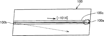
2After the dielectric film of making 112, using photoetching process to provide width by wet etching in dielectric film 112 is the banded window of 10 μ m.In this case owing to can in above-mentioned epitaxial loayer, indicate [1014] direction by datum level 12, so the direction of laser band from [1014] direction with-0.5 ° or bigger and 0.5 ° or littler angle tilt, as shown in Figure 23.
Because the opening (banded window) of dielectric film 112 is set on above-mentioned direction, therefore the orientation of the waveguide 100c of semiconductor laser device 100 be on [1014] direction or with respect to this direction towards [1-100] direction with-4 ° or bigger and 4 ° or littler angle tilt, and with the direction of [1-100] direction quadrature on-0.5 ° or bigger and 0.5 ° or littler angle tilt, as shown in Figure 23.In other words, with end face 100a and 100b ((1017) face, (10-1-7) face or with respect to these towards [1-100] direction with-4 ° or bigger and 4 ° or littler angle tilt and with the direction of [1-100] direction quadrature on the face of-0.5 ° or bigger and 0.5 ° or littler angle tilt) form waveguide 100c on the direction of approximate vertical.
Then, after banded window is provided, p type electrode 113 that vapour deposition is made by Ni/Au and the pad electrode (not shown) of making by Ti/Al.Then,, grind the back surface of cutting GaN substrate (nitride-based semiconductor substrate 10a), help the 100 μ m or the littler substrate thickness of cleavage, and make the substrate product of back surface with mirror status with realization by using diamond slurry.On the back surface (polished surface) of GaN substrate, form the n type electrode of making by Ti/Al/Ti/Au 114 by vapour deposition.
Use the resonator mirror that has adopted wavelength to be used for this laser band as the laser scribing means manufacturing of the YAG laser beam of 355nm.When laser scribing means is used to cut, compare with the situation of using the diamond scribing method, can improve vibration chip output capacity.Be set to 100mW and sweep speed is set under the condition of 5mm/s in laser output, form scribe line.For example, the length of resulting scribe line is 30 μ m, and width is that the 10 μ m and the degree of depth are 40 μ m.By being that pitch directly applies laser beam by the opening in the dielectric film of GaN substrate to the surface of epitaxial loayer with 800 μ m, form scribe line.Resonator length is set to 600 μ m.
Make the luminous mirror of resonator by using blade to cut.The downside that blade is pressed the GaN substrate is made laser strip thus with cutting substrate product.More specifically, as shown in Figure 24, end face 100a and the 100b that is used for laser resonator corresponds respectively to (1017) face and (10-1-7) face.First type surface 11, end face 100a and 100b are respectively with different such as traditional cleavage surface of traditional c face, m face and a face.
As the result of the face that utilizes sem observation to provide by cutting, do not observe significantly outstanding and depression.Therefore, the flatness size of depression (outstanding and) of supposing the face that obtains by cutting is 20nm or littler.In addition, the perpendicularity of sample surfaces with respect to above-mentioned fall into ± 5 ° scope in.
Then, by vacuum deposition method, the electricity consumption dielectric multilayer-film covers the end face of laser strip.By alternately laminated SiO
2(silicon dioxide) and TiO
2(titanium dioxide) forms the dielectric multilayer film.Film thickness is adjusted to and falls in 50nm or bigger and 100nm or the littler scope, is designed to fall in 500nm or bigger and 530nm or the littler scope with the centre wavelength with reflectivity.In a side, reflecting surface is set to 10 cycles, and the design load of reflectivity is set to about 95%.At opposite side, reflecting surface is set to 6 cycles, and the design load of reflectivity is set to about 80%.
Test and result
About the semiconductor laser device of structure as mentioned above, the first type surface of check GaN substrate with respect to (0001) towards tiltangle of [1-100] direction and the relation between the vibration output capacity.In this example, the vibration output capacity is defined as (quantity of vibration chip)/(quantity of measured chip).The result is shown in the table 1.
[table 1]
| ID | I-1 | I-2 | I-3 | I-4 | I-5 | I-6 | I-7 | I-8 | I-9 |
| The angle of first type surface (°) | 82 | 79 | 77 | 76 | 75 | 74 | 73 | 71 | 68 |
| The angle of chamfering (°) | 20 | 20 | 20 | 20 | 20 | 20 | 20 | 20 | 20 |
| Element output capacity (%) | 15 | 51 | 77 | 84 | 85 | 82 | 75 | 50 | 10 |
Table 1 shows excellent results, when promptly the tiltangle of the GaN substrate that forms between [0001] direction and [1-100] direction (angle of the first type surface of describing in the table 1) fell in 71 ° or bigger and 79 ° or the littler scope, the output capacity of vibrating was 50% or bigger.
(test 2)
In test 2, experimentize about substrate basically with above-mentioned tiltangle (angle of first type surface) of 75 °.Specifically, be under the situation of different angles check element output capacity and substrate output capacity in top side and back surface.Do not broken with substrate, fracture and the cracked corresponding substrate output capacity of percentage be defined as the quantity of fracture and cracked substrate (do not suffer visually to confirm observedly to break)/(quantity of the substrate of measurement).
The preparation of sample
By making the sample (the sample ID:II-1 to II-11 in the following table 2) of GaN substrate and the sample of semiconductor laser device with the basic similarly method of the sample that is used for making aforesaid test 1 preparation.Yet as shown in following table 2, the angle of first type surface (tiltangle) is set to 75 °, 71 ° or 79 °.In addition, for each sample, the chamfering of chamfered part changes in 0 ° to 60 ° scope, and is as shown in table 2.In this case, granularity is that the grinding stone of #1000 is used for chamfering.In addition, use substrate with same thickness.Shape shown in the Figure 11 that is mutually symmetrical based on the shape of top side and dorsal part wherein forms the shape (chamfer shape) of chamfered part.The chamfering amount is arranged on 0.2mm uniformly.
Test and result
About the sample of the GaN substrate made as mentioned above, by vision ground observe occur such as break, fracture and cracked situation calculate the substrate output capacity.In addition, the semiconductor laser device of making about each sample that uses the GaN substrate is measured vibration output capacity (element output capacity) in the mode identical with test 1.The result is shown in the table 2.
[table 2]
| ID | II-1 | II-2 | II-3 | II-4 | II-5 | II-6 | II-7 | II-8 | II-9 | II-10 | II-11 |
| The angle of first type surface (°) | 75 | 75 | 75 | 75 | 75 | 75 | 75 | 71 | 71 | 79 | 79 |
| The angle of chamfering (°) | 0 | 5 | 15 | 25 | 35 | 45 | 60 | 5 | 45 | 5 | 45 |
| Element output capacity (%) | 85 | 84 | 83 | 84 | 85 | 84 | 83 | 51 | 50 | 52 | 51 |
| Substrate output capacity (%) | 11 | 65 | 72 | 90 | 69 | 60 | 25 | 59 | 60 | 62 | 61 |
As shown in table 2, obtained excellent results, that is, and when the angle of chamfering is 5 ° or bigger and 45 ° or more hour, the substrate output capacity is 50%.In addition, between top surface and back surface, during all different chamfered part, also obtain similar result when the angle of using chamfering amount and chamfering.
In addition, when the angle (tiltangle) of first type surface falls in the scope of 71 ° and 79 °, also obtain similar result.About crystal, obtain the result identical equally with The above results by the solvent method growth.In addition, when a plurality of GaN substrates are used for underlying substrate when growing single GaN crystal by the HVPE method on a plurality of underlying substrate, also obtain the result identical with The above results.
[example 2]
In this example, be used under the different processing conditions of chamfered part (chamfer machining condition), the substrate that has the damaged layer of different-thickness in chamfered part is used to check the effect that is caused by damaged layer thickness.Specifically, the sample of preparation different GaN substrate of damaged layer thickness in chamfered part.Then, the manufacturing of use GaN substrate has the semiconductor laser device with example 1 same structure, and the check element output capacity.
The preparation of sample
Basically make the sample (the sample ID:III-1 to III-9 in the following table 3) of GaN substrate by the manufacture method identical with the manufacture method of GaN substrate in the example 1.The granularity etc. that is used for the rubber grinding stone of chamfer machining by adjusting changes the thickness of damaged layer.In addition, the GaN substrate is constructed to have the first type surface that tilts with the angle (angle of first type surface) of 75 ° or 73 ° towards [1-100] direction with respect to (0001).
Then, the same with example 1, use resulting GaN substrate to make semiconductor laser device.In addition, use substrate, and the shape shown in the Figure 11 that is mutually symmetrical based on the shape of top side and dorsal part wherein forms the shape (chamfer shape) of chamfered part with same thickness.Chamfer angle is arranged on 20 ° uniformly, and the chamfering amount is arranged on 0.2mm uniformly.
Test and result
About the semiconductor laser device of making, carry out oscillation experiment with the thickness (average damaged layer thickness) of damaged layer in the check chamfered part and the relation between the vibration output capacity (element output capacity).The result is shown in the table 3.
[table 3]
| ID | III-1 | III-2 | III-3 | III-4 | III-5 | III-6 | III-7 | III-8 | III-9 |
| The angle of first type surface (°) | 75 | 75 | 75 | 75 | 75 | 75 | 75 | 73 | 73 |
| The thickness of damaged layer in the chamfering (μ m) | 0.5 | 1 | 3 | 5 | 7 | 9 | 11 | 1 | 11 |
| Element output capacity (%) | 50 | 85 | 86 | 84 | 53 | 51 | 13 | 73 | 11 |
As shown in table 3, obtained excellent results, promptly the average damaged layer thickness in the chamfering is 0.5 μ m or bigger and 10 μ m or more hour, the element output capacity is 50% or bigger.In addition, when using chamfering amount and chamfer angle between top surface and back surface, during all different chamfered part, also to obtain identical result.About crystal, obtain the result identical equally with The above results by the solvent method growth.In addition, when a plurality of GaN substrates are used for underlying substrate when growing single GaN crystal by the HVPE method on a plurality of underlying substrate, also obtain the result identical with The above results.
[example 3]
In this example, be used under the different processing conditions of chamfered part (chamfer machining condition), having the substrate that carries out the chamfered part of chamfering with the difference amount and be used to check the effect that causes by the chamfering amount.Specifically, preparation has the sample of GaN substrate that carries out the chamfered part of chamfering with the difference amount, with check substrate output capacity.
The preparation of sample
Basically make the sample (the sample ID:IV-1 to IV-9 in the following table 4) of GaN substrate by the manufacture method identical with the manufacture method of GaN substrate in the example 1.The first type surface of GaN substrate is set at 75 ° or 74 ° with respect to (0001) towards the tiltangle (angle of first type surface) of [1-100] direction.In this case, granularity is that the grinding stone of #1000 is used for chamfering.In addition, use substrate, and the shape shown in the Figure 11 that is mutually symmetrical based on the shape of top side and dorsal part wherein forms the shape (chamfer shape) of chamfered part with same thickness.Chamfer angle is arranged on 20 ° uniformly.
Test and result
About the sample of the GaN substrate made as mentioned above, by vision ground observe occur such as break, the situation of fracture and cracked defective, calculate the substrate output capacity.The result is shown in the table 4.
[table 4]
| ID | IV-1 | IV-2 | IV-3 | IV-4 | IV-5 | IV-6 | IV-7 | IV-8 | IV-9 |
| The angle of first type surface (°) | 75 | 75 | 75 | 75 | 75 | 75 | 75 | 74 | 74 |
| Chamfering amount (mm) | 0 | 0.02 | 0.05 | 0.1 | 0.2 | 0.5 | 0.6 | 0.1 | 0.6 |
| Substrate output capacity (%) | 8 | 65 | 80 | 90 | 89 | 53 | 25 | 88 | 20 |
As shown in table 4, obtained excellent results, that is, and when the chamfering amount is 0.02mm or bigger and 0.5mm or more hour, the substrate output capacity is 50% or bigger.In addition, all between top surface and back surface, during different chamfered part, also obtain identical result when the angle of using chamfering amount and chamfering.About crystal, obtain the result identical equally with The above results by the solvent method growth.In addition, when a plurality of GaN substrates are used for underlying substrate when growing single GaN crystal by the HVPE method on a plurality of underlying substrate, also obtain the result identical with The above results.
[example 4]
In this example, be used under the different processing conditions of chamfered part (chamfer machining condition), the substrate that uses its chamfered part to have different surface roughness is checked the effect that is caused by surface roughness.Specifically, prepare the sample that its chamfered part has the GaN substrate of different surface roughness.Then, use the GaN substrate to make and semiconductor laser device, with the check element output capacity with same structure in the example 1.
The preparation of sample
Substantially by with example 1 in the identical manufacture method of manufacture method of GaN substrate, make the sample (the sample ID:V-1 to V-9 in the following table 5) of GaN substrate.In addition, be used for the granularity etc. of the rubber grinding stone of chamfer machining by adjusting, change the arithmetic average roughness (Ra) on the surface of chamfered part.In addition, the GaN substrate is configured to have the first type surface that tilts with the angle θ (angle of first type surface) of 75 ° or 76 ° towards [1-100] direction with respect to (0001).Use has the substrate of same thickness.Shape shown in the Figure 11 that is mutually symmetrical based on the shape of top side and dorsal part wherein forms the shape (chamfer shape) of chamfered part.Chamfer angle is arranged on 20 ° uniformly, and the chamfering amount is set to 0.2mm uniformly.
Then, use resulting GaN substrate, make semiconductor laser device in the mode identical with example 1.
Test and result
About the semiconductor laser device of manufacturing, carry out oscillation experiment, with the surface roughness (roughness of chamfering) of check chamfered part and the relation between the vibration output capacity (element output capacity).The result is shown in the table 5.
[table 5]
| ID | V-1 | V-2 | V-3 | V-4 | V-5 | V-6 | V-7 | V-8 | V-9 |
| The angle of first type surface (°) | 75 | 75 | 75 | 75 | 75 | 75 | 75 | 76 | 76 |
| The roughness Ra of chamfering (μ m) | 0.07 | 0.1 | 0.5 | 1 | 2 | 3 | 4 | 0.1 | 3 |
| Element output capacity (%) | 91 | 88 | 86 | 62 | 55 | 52 | 12 | 90 | 51 |
As shown in table 5, obtained excellent results, that is, and when the surface roughness of chamfered part is 0.07 μ m or bigger and 3 μ m or more hour, the element output capacity is 50% or bigger.In addition, when using chamfering amount and chamfer angle all between top surface and back surface, during different chamfered part, also to obtain identical result.About crystal, obtain the result identical equally with The above results by the solvent method growth.In addition, when a plurality of GaN substrates are used for underlying substrate when growing single GaN crystal by the HVPE method on a plurality of underlying substrate, also obtain the result identical with The above results.
The present invention particularly advantageously is applied to have the nitride-based semiconductor substrate and the semiconductor device that uses this nitride-based semiconductor substrate to make as the first type surface of semi-polarity face.
Though described and shown the present invention in detail, clear being understood that, this explain scope of the present invention according to claim just the description of carrying out with the mode of example rather than restriction to be shown and to illustrate.
Claims (7)
1. nitride-based semiconductor substrate comprises:
First type surface, described first type surface with respect to (0001) towards [1-100] direction with 71 ° or bigger and 79 ° or littler angle tilt, perhaps with respect to (000-1) towards [1100] direction with 71 ° or bigger and 79 ° or littler angle tilt; And
Chamfered part, described chamfered part is positioned at the edge of the periphery of described first type surface,
Described chamfered part with respect in the back surface on described first type surface and the side opposite with described first type surface adjacent one with 5 ° or bigger and 45 ° or littler angle tilt.
2. nitride-based semiconductor substrate according to claim 1, wherein forming average thickness on the superficial layer of described chamfered part is 0.5 μ m or bigger and 10 μ m or littler damaged layer.
3. nitride-based semiconductor substrate according to claim 1, the chamfering amount of wherein said chamfered part are 0.02mm or bigger and 0.5mm or littler.
4. nitride-based semiconductor substrate according to claim 1, the surface roughness Ra of wherein said chamfered part are 0.07 μ m or bigger and 3 μ m or littler.
5. semiconductor device that uses nitride-based semiconductor substrate according to claim 1 to make.
6. a method that is used to make the nitride-based semiconductor substrate comprises the steps:
Preparation has the nitride-based semiconductor substrate of first type surface, described first type surface with respect to (0001) towards [1-100] direction with 71 ° or bigger and 79 ° or littler angle tilt or with respect to (000-1) towards [1100] direction with 71 ° or bigger and 79 ° or littler angle tilt; And
The edge of the periphery of the described first type surface of the described nitride-based semiconductor substrate of chamfering,
The described step at the described edge of chamfering comprises that formation is with respect to an adjacent step with the chamfered part of 5 ° or bigger and 45 ° or littler angle tilt in the back surface on described first type surface and the side opposite with described first type surface.
7. a method that is used for producing the semiconductor devices comprises the steps:
Use the method that is used to make nitride compound semiconductor device according to claim 6 to prepare the nitride-based semiconductor substrate; And
On the described first type surface of described nitride-based semiconductor substrate, form epitaxial loayer.
Applications Claiming Priority (2)
| Application Number | Priority Date | Filing Date | Title |
|---|---|---|---|
| JP2009-218890 | 2009-09-24 | ||
| JP2009218890A JP5040977B2 (en) | 2009-09-24 | 2009-09-24 | Nitride semiconductor substrate, semiconductor device and manufacturing method thereof |
Publications (1)
| Publication Number | Publication Date |
|---|---|
| CN102034853A true CN102034853A (en) | 2011-04-27 |
Family
ID=43217049
Family Applications (1)
| Application Number | Title | Priority Date | Filing Date |
|---|---|---|---|
| CN2010102329617A Pending CN102034853A (en) | 2009-09-24 | 2010-07-16 | Nitride semiconductor substrate, semiconductor device, and methods for manufacturing nitride semiconductor substrate and semiconductor device |
Country Status (5)
| Country | Link |
|---|---|
| US (2) | US8471365B2 (en) |
| EP (1) | EP2302113A1 (en) |
| JP (1) | JP5040977B2 (en) |
| CN (1) | CN102034853A (en) |
| TW (1) | TWI550903B (en) |
Cited By (6)
| Publication number | Priority date | Publication date | Assignee | Title |
|---|---|---|---|---|
| CN103374754A (en) * | 2012-04-17 | 2013-10-30 | 鑫晶钻科技股份有限公司 | Sapphire material and preparation method thereof |
| CN103959579A (en) * | 2011-12-08 | 2014-07-30 | 索尼公司 | Method for manufacturing semiconductor laser element, and semiconductor laser element |
| CN107305920A (en) * | 2016-04-20 | 2017-10-31 | 晶元光电股份有限公司 | Substrate wafer and method for manufacturing group III nitride semiconductor device |
| CN107623028A (en) * | 2016-07-13 | 2018-01-23 | 环球晶圆股份有限公司 | Semiconductor substrate and processing method thereof |
| CN109390383A (en) * | 2017-08-04 | 2019-02-26 | 财团法人工业技术研究院 | epitaxial wafer |
| CN112820633A (en) * | 2021-01-14 | 2021-05-18 | 镓特半导体科技(上海)有限公司 | Gallium nitride layer and homoepitaxial growth method thereof |
Families Citing this family (15)
| Publication number | Priority date | Publication date | Assignee | Title |
|---|---|---|---|---|
| JP5381581B2 (en) * | 2009-09-30 | 2014-01-08 | 住友電気工業株式会社 | Gallium nitride substrate |
| JP6031733B2 (en) * | 2010-09-27 | 2016-11-24 | 住友電気工業株式会社 | GaN crystal manufacturing method |
| JP5808208B2 (en) * | 2011-09-15 | 2015-11-10 | 株式会社サイオクス | Manufacturing method of nitride semiconductor substrate |
| US8471366B2 (en) * | 2011-11-30 | 2013-06-25 | Sumitomo Electric Industries, Ltd. | Nitride semiconductor substrate |
| JP5982971B2 (en) * | 2012-04-10 | 2016-08-31 | 住友電気工業株式会社 | Silicon carbide single crystal substrate |
| US9040421B2 (en) * | 2013-05-03 | 2015-05-26 | GlobalFoundries, Inc. | Methods for fabricating integrated circuits with improved contact structures |
| JP5950070B1 (en) * | 2014-12-16 | 2016-07-13 | 三菱化学株式会社 | GaN substrate |
| JP6851017B2 (en) | 2016-05-18 | 2021-03-31 | パナソニックIpマネジメント株式会社 | Device and its manufacturing method |
| TWI626340B (en) * | 2016-07-13 | 2018-06-11 | 環球晶圓股份有限公司 | Semiconductor substrate and manufacturing method thereof |
| JP6149988B2 (en) * | 2016-08-01 | 2017-06-21 | 住友電気工業株式会社 | Silicon carbide single crystal substrate |
| US10186630B2 (en) * | 2016-08-02 | 2019-01-22 | QMAT, Inc. | Seed wafer for GaN thickening using gas- or liquid-phase epitaxy |
| US10505087B2 (en) * | 2017-08-24 | 2019-12-10 | Soko Kagaku Co., Ltd. | Method for manufacturing nitride semiconductor ultraviolet light-emitting element and nitride semiconductor ultraviolet light-emitting element |
| DE112021003545T5 (en) * | 2020-09-17 | 2023-04-20 | Ngk Insulators, Ltd. | Group III nitride semiconductor substrate |
| JP7150199B1 (en) * | 2021-06-30 | 2022-10-07 | 京セラ株式会社 | METHOD FOR MANUFACTURING GALLIUM NITRIDE SINGLE CRYSTAL SUBSTRATE AND METHOD FOR MANUFACTURING GROUP 13 NITRIDE NITORIED SINGLE CRYSTAL SUBSTRATE OF PERIODIC TABLE |
| WO2023176128A1 (en) * | 2022-03-14 | 2023-09-21 | 日本碍子株式会社 | Group iii element nitride semiconductor substrate and laminated substrate |
Citations (9)
| Publication number | Priority date | Publication date | Assignee | Title |
|---|---|---|---|---|
| WO1991007567A1 (en) * | 1989-11-15 | 1991-05-30 | Atlantic Richfield Company | Tubing conveyed wellbore fluid flow measurement apparatus |
| JP2002222746A (en) * | 2001-01-23 | 2002-08-09 | Matsushita Electric Ind Co Ltd | Nitride semiconductor wafer and its manufacturing method |
| JP2002356398A (en) * | 2001-06-01 | 2002-12-13 | Sumitomo Electric Ind Ltd | Gallium nitride wafer |
| US6756426B2 (en) * | 2001-12-20 | 2004-06-29 | I-Tek, Inc. | Lightweight composite material for protective pads, cushions, supports or the like and method |
| JP2004319951A (en) * | 2003-04-02 | 2004-11-11 | Sumitomo Electric Ind Ltd | EDGE POLISHED NITRIDE SEMICONDUCTOR SUBSTRATE, EDGE POLISHED GaN FREE-STANDING SUBSTRATE, AND EDGE PROCESSING METHOD OF NITRIDE SEMICONDUCTOR SUBSTRATE |
| CN1612290A (en) * | 2003-10-30 | 2005-05-04 | 住友电气工业株式会社 | Method of manufacturing nitride substrate for semiconductors, and nitride semiconductor substrate |
| CN101043121A (en) * | 2006-03-22 | 2007-09-26 | 三洋电机株式会社 | Method of fabricating nitride-based semiconductor light-emitting device and nitride-based semiconductor light-emitting device |
| WO2009107567A1 (en) * | 2008-02-27 | 2009-09-03 | 住友電気工業株式会社 | Method for machining nitride semiconductor wafer, nitride semiconductor wafer, process for producing nitride semiconductor device, and nitride semiconductor device |
| CN102112666A (en) * | 2009-01-19 | 2011-06-29 | 住友电气工业株式会社 | Compound semiconductor substrate, semiconductor device, and process for producing semiconductor device |
Family Cites Families (5)
| Publication number | Priority date | Publication date | Assignee | Title |
|---|---|---|---|---|
| JPH04333820A (en) | 1991-05-10 | 1992-11-20 | Sony Corp | Characteristic evaluation device for two-dimensional display element |
| JP4595198B2 (en) * | 2000-12-15 | 2010-12-08 | ソニー株式会社 | Semiconductor light emitting device and method for manufacturing semiconductor light emitting device |
| JP2003077847A (en) * | 2001-09-06 | 2003-03-14 | Sumitomo Chem Co Ltd | Manufacturing method of 3-5 compound semiconductor |
| US20070221932A1 (en) * | 2006-03-22 | 2007-09-27 | Sanyo Electric Co., Ltd. | Method of fabricating nitride-based semiconductor light-emitting device and nitride-based semiconductor light-emitting device |
| JP4928874B2 (en) * | 2006-08-31 | 2012-05-09 | 三洋電機株式会社 | Nitride-based semiconductor light-emitting device manufacturing method and nitride-based semiconductor light-emitting device |
-
2009
- 2009-09-24 JP JP2009218890A patent/JP5040977B2/en active Active
-
2010
- 2010-06-30 TW TW099121576A patent/TWI550903B/en active
- 2010-07-01 EP EP20100168041 patent/EP2302113A1/en not_active Withdrawn
- 2010-07-09 US US12/833,145 patent/US8471365B2/en active Active
- 2010-07-16 CN CN2010102329617A patent/CN102034853A/en active Pending
-
2013
- 2013-05-16 US US13/895,924 patent/US20130252401A1/en not_active Abandoned
Patent Citations (9)
| Publication number | Priority date | Publication date | Assignee | Title |
|---|---|---|---|---|
| WO1991007567A1 (en) * | 1989-11-15 | 1991-05-30 | Atlantic Richfield Company | Tubing conveyed wellbore fluid flow measurement apparatus |
| JP2002222746A (en) * | 2001-01-23 | 2002-08-09 | Matsushita Electric Ind Co Ltd | Nitride semiconductor wafer and its manufacturing method |
| JP2002356398A (en) * | 2001-06-01 | 2002-12-13 | Sumitomo Electric Ind Ltd | Gallium nitride wafer |
| US6756426B2 (en) * | 2001-12-20 | 2004-06-29 | I-Tek, Inc. | Lightweight composite material for protective pads, cushions, supports or the like and method |
| JP2004319951A (en) * | 2003-04-02 | 2004-11-11 | Sumitomo Electric Ind Ltd | EDGE POLISHED NITRIDE SEMICONDUCTOR SUBSTRATE, EDGE POLISHED GaN FREE-STANDING SUBSTRATE, AND EDGE PROCESSING METHOD OF NITRIDE SEMICONDUCTOR SUBSTRATE |
| CN1612290A (en) * | 2003-10-30 | 2005-05-04 | 住友电气工业株式会社 | Method of manufacturing nitride substrate for semiconductors, and nitride semiconductor substrate |
| CN101043121A (en) * | 2006-03-22 | 2007-09-26 | 三洋电机株式会社 | Method of fabricating nitride-based semiconductor light-emitting device and nitride-based semiconductor light-emitting device |
| WO2009107567A1 (en) * | 2008-02-27 | 2009-09-03 | 住友電気工業株式会社 | Method for machining nitride semiconductor wafer, nitride semiconductor wafer, process for producing nitride semiconductor device, and nitride semiconductor device |
| CN102112666A (en) * | 2009-01-19 | 2011-06-29 | 住友电气工业株式会社 | Compound semiconductor substrate, semiconductor device, and process for producing semiconductor device |
Cited By (9)
| Publication number | Priority date | Publication date | Assignee | Title |
|---|---|---|---|---|
| CN103959579A (en) * | 2011-12-08 | 2014-07-30 | 索尼公司 | Method for manufacturing semiconductor laser element, and semiconductor laser element |
| CN103374754A (en) * | 2012-04-17 | 2013-10-30 | 鑫晶钻科技股份有限公司 | Sapphire material and preparation method thereof |
| CN107305920A (en) * | 2016-04-20 | 2017-10-31 | 晶元光电股份有限公司 | Substrate wafer and method for manufacturing group III nitride semiconductor device |
| CN107305920B (en) * | 2016-04-20 | 2020-04-07 | 晶元光电股份有限公司 | Substrate wafer and method for manufacturing group III nitride semiconductor device |
| CN107623028A (en) * | 2016-07-13 | 2018-01-23 | 环球晶圆股份有限公司 | Semiconductor substrate and processing method thereof |
| CN107623028B (en) * | 2016-07-13 | 2021-02-19 | 环球晶圆股份有限公司 | Semiconductor substrate and processing method thereof |
| CN109390383A (en) * | 2017-08-04 | 2019-02-26 | 财团法人工业技术研究院 | epitaxial wafer |
| CN112820633A (en) * | 2021-01-14 | 2021-05-18 | 镓特半导体科技(上海)有限公司 | Gallium nitride layer and homoepitaxial growth method thereof |
| CN112820633B (en) * | 2021-01-14 | 2024-01-16 | 镓特半导体科技(上海)有限公司 | Gallium nitride layer and homoepitaxial growth method thereof |
Also Published As
| Publication number | Publication date |
|---|---|
| TW201121096A (en) | 2011-06-16 |
| TWI550903B (en) | 2016-09-21 |
| EP2302113A1 (en) | 2011-03-30 |
| US20110068434A1 (en) | 2011-03-24 |
| US8471365B2 (en) | 2013-06-25 |
| JP2011071180A (en) | 2011-04-07 |
| US20130252401A1 (en) | 2013-09-26 |
| JP5040977B2 (en) | 2012-10-03 |
Similar Documents
| Publication | Publication Date | Title |
|---|---|---|
| CN102034853A (en) | Nitride semiconductor substrate, semiconductor device, and methods for manufacturing nitride semiconductor substrate and semiconductor device | |
| JP4333820B1 (en) | Compound semiconductor substrate | |
| EP1736574B1 (en) | Nitride crystal, epilayer-containing nitride crystal substrate, semiconductor device and method of manufacturing the same | |
| TWI433224B (en) | Method for processing nitride semiconductor wafers, nitride semiconductor wafers, fabrication of nitride semiconductor elements, and nitride semiconductor elements | |
| US10612161B2 (en) | GaN substrate | |
| US9499925B2 (en) | Group III nitride crystal substrate, epilayer-containing group III nitride crystal substrate, semiconductor device and method of manufacturing the same | |
| EP1897978A1 (en) | Manufacturing method of group III nitride substrate, group III nitride substrate, group III nitride substrate with epitaxial layer, group III nitride device, manufacturing method of group III nidtride substrate with epitaxial layer, and manufacturing method of group III nitride device | |
| JP4835749B2 (en) | Group III nitride crystal substrate, group III nitride crystal substrate with epi layer, and semiconductor device and method for manufacturing the same | |
| JP5233936B2 (en) | Nitride semiconductor substrate | |
| US10113248B2 (en) | Group III nitride crystal substrate, epilayer-containing group III nitride crystal substrate, semiconductor device and method of manufacturing the same | |
| TW201417148A (en) | Group iii nitride composite substrate, manufacturing method therefor, and group iii nitride semiconductor device manufacturing method | |
| CN104995713A (en) | Group iii-nitride composite substrate and method of producing same, layered group iii-nitride composite substrate, as well as group iii-nitride semiconductor device and method of producing same | |
| JP6135441B2 (en) | Group III nitride composite substrate and method for manufacturing the same, laminated group III nitride composite substrate, group III nitride semiconductor device and method for manufacturing the same | |
| US8124969B2 (en) | Semiconductor light emitting element and method for manufacturing the same | |
| JP5045292B2 (en) | Manufacturing method of nitride semiconductor substrate | |
| WO2015053127A1 (en) | Group-iii-nitride composite substrate, production method therefor, laminated group-iii-nitride composite substrate, and group-iii-nitride semiconductor device and production method therefor | |
| JP5141809B2 (en) | Semiconductor laser | |
| US20120223417A1 (en) | Group iii nitride crystal substrate, epilayer-containing group iii nitride crystal substrate, semiconductor device and method of manufacturing the same | |
| JP5636642B2 (en) | Compound semiconductor substrate | |
| JP2014157983A (en) | Group iii nitride composite substrate, method for manufacturing the same, lamination group iii nitride composite substrate, group iii nitride semiconductor device and method for manufacturing the same | |
| JP2011251909A (en) | Nitride semiconductor substrate | |
| JP2013138259A (en) | Nitride semiconductor substrate |
Legal Events
| Date | Code | Title | Description |
|---|---|---|---|
| C06 | Publication | ||
| PB01 | Publication | ||
| C10 | Entry into substantive examination | ||
| SE01 | Entry into force of request for substantive examination | ||
| C02 | Deemed withdrawal of patent application after publication (patent law 2001) | ||
| WD01 | Invention patent application deemed withdrawn after publication |
Application publication date: 20110427 |