CN101197394B - Semiconductor device and manufacturing method thereof - Google Patents
Semiconductor device and manufacturing method thereof Download PDFInfo
- Publication number
- CN101197394B CN101197394B CN2007101964822A CN200710196482A CN101197394B CN 101197394 B CN101197394 B CN 101197394B CN 2007101964822 A CN2007101964822 A CN 2007101964822A CN 200710196482 A CN200710196482 A CN 200710196482A CN 101197394 B CN101197394 B CN 101197394B
- Authority
- CN
- China
- Prior art keywords
- insulating barrier
- silicon layer
- layer
- island
- contacted
- Prior art date
- Legal status (The legal status is an assumption and is not a legal conclusion. Google has not performed a legal analysis and makes no representation as to the accuracy of the status listed.)
- Expired - Fee Related
Links
- 239000004065 semiconductor Substances 0.000 title claims abstract description 209
- 238000004519 manufacturing process Methods 0.000 title claims abstract description 71
- 239000000758 substrate Substances 0.000 claims abstract description 147
- 230000004888 barrier function Effects 0.000 claims description 659
- 238000005530 etching Methods 0.000 claims description 182
- 238000009413 insulation Methods 0.000 claims description 163
- 230000015572 biosynthetic process Effects 0.000 claims description 114
- 238000013459 approach Methods 0.000 claims description 60
- 238000000034 method Methods 0.000 claims description 53
- QVGXLLKOCUKJST-UHFFFAOYSA-N atomic oxygen Chemical compound [O] QVGXLLKOCUKJST-UHFFFAOYSA-N 0.000 claims description 22
- 229910052760 oxygen Inorganic materials 0.000 claims description 22
- 239000001301 oxygen Substances 0.000 claims description 22
- 238000005452 bending Methods 0.000 claims description 12
- 239000013078 crystal Substances 0.000 claims 10
- 229910052710 silicon Inorganic materials 0.000 abstract description 807
- 239000010703 silicon Substances 0.000 abstract description 807
- XUIMIQQOPSSXEZ-UHFFFAOYSA-N Silicon Chemical compound [Si] XUIMIQQOPSSXEZ-UHFFFAOYSA-N 0.000 abstract description 803
- 230000007547 defect Effects 0.000 abstract description 9
- 239000010410 layer Substances 0.000 description 1272
- 239000012535 impurity Substances 0.000 description 215
- 239000010408 film Substances 0.000 description 98
- VYPSYNLAJGMNEJ-UHFFFAOYSA-N Silicium dioxide Chemical compound O=[Si]=O VYPSYNLAJGMNEJ-UHFFFAOYSA-N 0.000 description 70
- 239000007789 gas Substances 0.000 description 70
- 239000000463 material Substances 0.000 description 69
- IJGRMHOSHXDMSA-UHFFFAOYSA-N Atomic nitrogen Chemical compound N#N IJGRMHOSHXDMSA-UHFFFAOYSA-N 0.000 description 49
- 239000010409 thin film Substances 0.000 description 46
- 239000012467 final product Substances 0.000 description 44
- 230000005684 electric field Effects 0.000 description 34
- 230000002950 deficient Effects 0.000 description 33
- 239000000377 silicon dioxide Substances 0.000 description 30
- 238000005229 chemical vapour deposition Methods 0.000 description 26
- 238000004544 sputter deposition Methods 0.000 description 26
- 229910052757 nitrogen Inorganic materials 0.000 description 24
- 239000010936 titanium Substances 0.000 description 22
- 239000004411 aluminium Substances 0.000 description 21
- 229910052782 aluminium Inorganic materials 0.000 description 21
- XAGFODPZIPBFFR-UHFFFAOYSA-N aluminium Chemical compound [Al] XAGFODPZIPBFFR-UHFFFAOYSA-N 0.000 description 21
- 230000015556 catabolic process Effects 0.000 description 21
- 239000010949 copper Substances 0.000 description 20
- 229910052581 Si3N4 Inorganic materials 0.000 description 19
- 239000004568 cement Substances 0.000 description 19
- 239000002131 composite material Substances 0.000 description 19
- 229910052751 metal Inorganic materials 0.000 description 19
- HQVNEWCFYHHQES-UHFFFAOYSA-N silicon nitride Chemical compound N12[Si]34N5[Si]62N3[Si]51N64 HQVNEWCFYHHQES-UHFFFAOYSA-N 0.000 description 19
- 239000002356 single layer Substances 0.000 description 19
- 229910021421 monocrystalline silicon Inorganic materials 0.000 description 18
- 230000003647 oxidation Effects 0.000 description 18
- 238000007254 oxidation reaction Methods 0.000 description 18
- OAICVXFJPJFONN-UHFFFAOYSA-N Phosphorus Chemical compound [P] OAICVXFJPJFONN-UHFFFAOYSA-N 0.000 description 16
- 229910052698 phosphorus Inorganic materials 0.000 description 16
- 239000011574 phosphorus Substances 0.000 description 16
- 229910052786 argon Inorganic materials 0.000 description 15
- BSYNRYMUTXBXSQ-UHFFFAOYSA-N Aspirin Chemical compound CC(=O)OC1=CC=CC=C1C(O)=O BSYNRYMUTXBXSQ-UHFFFAOYSA-N 0.000 description 14
- 239000011651 chromium Substances 0.000 description 14
- 239000010955 niobium Substances 0.000 description 14
- PXHVJJICTQNCMI-UHFFFAOYSA-N Nickel Chemical compound [Ni] PXHVJJICTQNCMI-UHFFFAOYSA-N 0.000 description 13
- 238000005280 amorphization Methods 0.000 description 13
- 238000001020 plasma etching Methods 0.000 description 13
- ZOKXTWBITQBERF-UHFFFAOYSA-N Molybdenum Chemical compound [Mo] ZOKXTWBITQBERF-UHFFFAOYSA-N 0.000 description 12
- RTAQQCXQSZGOHL-UHFFFAOYSA-N Titanium Chemical compound [Ti] RTAQQCXQSZGOHL-UHFFFAOYSA-N 0.000 description 12
- 239000000853 adhesive Substances 0.000 description 12
- 230000001070 adhesive effect Effects 0.000 description 12
- 229910052796 boron Inorganic materials 0.000 description 12
- 229910052799 carbon Inorganic materials 0.000 description 12
- 239000012141 concentrate Substances 0.000 description 12
- 229910052750 molybdenum Inorganic materials 0.000 description 12
- 239000011733 molybdenum Substances 0.000 description 12
- 239000000047 product Substances 0.000 description 12
- 229910052719 titanium Inorganic materials 0.000 description 12
- ZOXJGFHDIHLPTG-UHFFFAOYSA-N Boron Chemical compound [B] ZOXJGFHDIHLPTG-UHFFFAOYSA-N 0.000 description 11
- 239000000956 alloy Substances 0.000 description 11
- 229910052734 helium Inorganic materials 0.000 description 11
- 238000012545 processing Methods 0.000 description 11
- 239000007790 solid phase Substances 0.000 description 11
- RYGMFSIKBFXOCR-UHFFFAOYSA-N Copper Chemical compound [Cu] RYGMFSIKBFXOCR-UHFFFAOYSA-N 0.000 description 10
- 229910052802 copper Inorganic materials 0.000 description 10
- 230000001590 oxidative effect Effects 0.000 description 10
- 230000003071 parasitic effect Effects 0.000 description 10
- 239000012071 phase Substances 0.000 description 10
- 229910052814 silicon oxide Inorganic materials 0.000 description 10
- 229910052715 tantalum Inorganic materials 0.000 description 10
- GUVRBAGPIYLISA-UHFFFAOYSA-N tantalum atom Chemical compound [Ta] GUVRBAGPIYLISA-UHFFFAOYSA-N 0.000 description 10
- 229910052721 tungsten Inorganic materials 0.000 description 10
- 239000010937 tungsten Substances 0.000 description 10
- 229910017083 AlN Inorganic materials 0.000 description 9
- PIGFYZPCRLYGLF-UHFFFAOYSA-N Aluminum nitride Chemical compound [Al]#N PIGFYZPCRLYGLF-UHFFFAOYSA-N 0.000 description 9
- 238000010586 diagram Methods 0.000 description 9
- 238000005516 engineering process Methods 0.000 description 9
- 239000011261 inert gas Substances 0.000 description 9
- BASFCYQUMIYNBI-UHFFFAOYSA-N platinum Chemical compound [Pt] BASFCYQUMIYNBI-UHFFFAOYSA-N 0.000 description 9
- 229920005989 resin Polymers 0.000 description 9
- 239000011347 resin Substances 0.000 description 9
- KRHYYFGTRYWZRS-UHFFFAOYSA-N Fluorane Chemical compound F KRHYYFGTRYWZRS-UHFFFAOYSA-N 0.000 description 8
- YCKRFDGAMUMZLT-UHFFFAOYSA-N Fluorine atom Chemical compound [F] YCKRFDGAMUMZLT-UHFFFAOYSA-N 0.000 description 8
- MWUXSHHQAYIFBG-UHFFFAOYSA-N Nitric oxide Chemical compound O=[N] MWUXSHHQAYIFBG-UHFFFAOYSA-N 0.000 description 8
- 229910020177 SiOF Inorganic materials 0.000 description 8
- 229910052731 fluorine Inorganic materials 0.000 description 8
- 239000011737 fluorine Substances 0.000 description 8
- 230000008569 process Effects 0.000 description 8
- WFKWXMTUELFFGS-UHFFFAOYSA-N tungsten Chemical compound [W] WFKWXMTUELFFGS-UHFFFAOYSA-N 0.000 description 8
- VYZAMTAEIAYCRO-UHFFFAOYSA-N Chromium Chemical compound [Cr] VYZAMTAEIAYCRO-UHFFFAOYSA-N 0.000 description 7
- GYHNNYVSQQEPJS-UHFFFAOYSA-N Gallium Chemical compound [Ga] GYHNNYVSQQEPJS-UHFFFAOYSA-N 0.000 description 7
- 229910021417 amorphous silicon Inorganic materials 0.000 description 7
- 229910052785 arsenic Inorganic materials 0.000 description 7
- RQNWIZPPADIBDY-UHFFFAOYSA-N arsenic atom Chemical compound [As] RQNWIZPPADIBDY-UHFFFAOYSA-N 0.000 description 7
- 229910052804 chromium Inorganic materials 0.000 description 7
- 238000002425 crystallisation Methods 0.000 description 7
- 230000008025 crystallization Effects 0.000 description 7
- 229910052733 gallium Inorganic materials 0.000 description 7
- 238000010438 heat treatment Methods 0.000 description 7
- 229910052758 niobium Inorganic materials 0.000 description 7
- GUCVJGMIXFAOAE-UHFFFAOYSA-N niobium atom Chemical compound [Nb] GUCVJGMIXFAOAE-UHFFFAOYSA-N 0.000 description 7
- 229910021420 polycrystalline silicon Inorganic materials 0.000 description 7
- 229920005591 polysilicon Polymers 0.000 description 7
- KDLHZDBZIXYQEI-UHFFFAOYSA-N Palladium Chemical compound [Pd] KDLHZDBZIXYQEI-UHFFFAOYSA-N 0.000 description 6
- 230000004913 activation Effects 0.000 description 6
- 238000000137 annealing Methods 0.000 description 6
- 150000001875 compounds Chemical class 0.000 description 6
- 239000010931 gold Substances 0.000 description 6
- 239000012528 membrane Substances 0.000 description 6
- QJGQUHMNIGDVPM-UHFFFAOYSA-N nitrogen group Chemical group [N] QJGQUHMNIGDVPM-UHFFFAOYSA-N 0.000 description 6
- 239000002245 particle Substances 0.000 description 6
- 238000010301 surface-oxidation reaction Methods 0.000 description 6
- -1 tungsten nitride Chemical class 0.000 description 6
- 229910052724 xenon Inorganic materials 0.000 description 6
- 235000018734 Sambucus australis Nutrition 0.000 description 5
- 244000180577 Sambucus australis Species 0.000 description 5
- 230000003213 activating effect Effects 0.000 description 5
- 239000000460 chlorine Substances 0.000 description 5
- 239000003814 drug Substances 0.000 description 5
- 235000013305 food Nutrition 0.000 description 5
- OGFXBIXJCWAUCH-UHFFFAOYSA-N meso-secoisolariciresinol Natural products C1=2C=C(O)C(OC)=CC=2CC(CO)C(CO)C1C1=CC=C(O)C(OC)=C1 OGFXBIXJCWAUCH-UHFFFAOYSA-N 0.000 description 5
- 229910052759 nickel Inorganic materials 0.000 description 5
- 238000012856 packing Methods 0.000 description 5
- 229910052709 silver Inorganic materials 0.000 description 5
- 239000004332 silver Substances 0.000 description 5
- XKRFYHLGVUSROY-UHFFFAOYSA-N Argon Chemical compound [Ar] XKRFYHLGVUSROY-UHFFFAOYSA-N 0.000 description 4
- GQPLMRYTRLFLPF-UHFFFAOYSA-N Nitrous Oxide Chemical compound [O-][N+]#N GQPLMRYTRLFLPF-UHFFFAOYSA-N 0.000 description 4
- BQCADISMDOOEFD-UHFFFAOYSA-N Silver Chemical compound [Ag] BQCADISMDOOEFD-UHFFFAOYSA-N 0.000 description 4
- KMWBBMXGHHLDKL-UHFFFAOYSA-N [AlH3].[Si] Chemical compound [AlH3].[Si] KMWBBMXGHHLDKL-UHFFFAOYSA-N 0.000 description 4
- 239000001257 hydrogen Substances 0.000 description 4
- 229910052739 hydrogen Inorganic materials 0.000 description 4
- 229910052743 krypton Inorganic materials 0.000 description 4
- 239000003595 mist Substances 0.000 description 4
- 238000000926 separation method Methods 0.000 description 4
- 150000003376 silicon Chemical class 0.000 description 4
- 238000005406 washing Methods 0.000 description 4
- OKTJSMMVPCPJKN-UHFFFAOYSA-N Carbon Chemical compound [C] OKTJSMMVPCPJKN-UHFFFAOYSA-N 0.000 description 3
- UFHFLCQGNIYNRP-UHFFFAOYSA-N Hydrogen Chemical compound [H][H] UFHFLCQGNIYNRP-UHFFFAOYSA-N 0.000 description 3
- 230000001143 conditioned effect Effects 0.000 description 3
- 230000005669 field effect Effects 0.000 description 3
- PCHJSUWPFVWCPO-UHFFFAOYSA-N gold Chemical compound [Au] PCHJSUWPFVWCPO-UHFFFAOYSA-N 0.000 description 3
- 229910052737 gold Inorganic materials 0.000 description 3
- 230000036541 health Effects 0.000 description 3
- 239000011810 insulating material Substances 0.000 description 3
- 238000002955 isolation Methods 0.000 description 3
- 229910052697 platinum Inorganic materials 0.000 description 3
- 229920001296 polysiloxane Polymers 0.000 description 3
- 230000003068 static effect Effects 0.000 description 3
- MGWGWNFMUOTEHG-UHFFFAOYSA-N 4-(3,5-dimethylphenyl)-1,3-thiazol-2-amine Chemical compound CC1=CC(C)=CC(C=2N=C(N)SC=2)=C1 MGWGWNFMUOTEHG-UHFFFAOYSA-N 0.000 description 2
- 241000293849 Cordylanthus Species 0.000 description 2
- CBENFWSGALASAD-UHFFFAOYSA-N Ozone Chemical compound [O-][O+]=O CBENFWSGALASAD-UHFFFAOYSA-N 0.000 description 2
- NRTOMJZYCJJWKI-UHFFFAOYSA-N Titanium nitride Chemical compound [Ti]#N NRTOMJZYCJJWKI-UHFFFAOYSA-N 0.000 description 2
- 125000004429 atom Chemical group 0.000 description 2
- 230000008859 change Effects 0.000 description 2
- 238000003486 chemical etching Methods 0.000 description 2
- 239000004020 conductor Substances 0.000 description 2
- 230000000694 effects Effects 0.000 description 2
- 239000000284 extract Substances 0.000 description 2
- 229910010272 inorganic material Inorganic materials 0.000 description 2
- 239000011147 inorganic material Substances 0.000 description 2
- 239000011572 manganese Substances 0.000 description 2
- 239000000203 mixture Substances 0.000 description 2
- 229910052754 neon Inorganic materials 0.000 description 2
- 150000004767 nitrides Chemical class 0.000 description 2
- JCXJVPUVTGWSNB-UHFFFAOYSA-N nitrogen dioxide Inorganic materials O=[N]=O JCXJVPUVTGWSNB-UHFFFAOYSA-N 0.000 description 2
- 239000001272 nitrous oxide Substances 0.000 description 2
- 125000000962 organic group Chemical group 0.000 description 2
- 239000011368 organic material Substances 0.000 description 2
- 229910052763 palladium Inorganic materials 0.000 description 2
- 238000009832 plasma treatment Methods 0.000 description 2
- 238000007639 printing Methods 0.000 description 2
- 150000003254 radicals Chemical class 0.000 description 2
- 229910000679 solder Inorganic materials 0.000 description 2
- 238000000992 sputter etching Methods 0.000 description 2
- 239000011800 void material Substances 0.000 description 2
- 101100113692 Caenorhabditis elegans clk-2 gene Proteins 0.000 description 1
- 102100040862 Dual specificity protein kinase CLK1 Human genes 0.000 description 1
- 102100040844 Dual specificity protein kinase CLK2 Human genes 0.000 description 1
- 239000004593 Epoxy Substances 0.000 description 1
- 101000749294 Homo sapiens Dual specificity protein kinase CLK1 Proteins 0.000 description 1
- 101000749291 Homo sapiens Dual specificity protein kinase CLK2 Proteins 0.000 description 1
- PWHULOQIROXLJO-UHFFFAOYSA-N Manganese Chemical compound [Mn] PWHULOQIROXLJO-UHFFFAOYSA-N 0.000 description 1
- 229910052779 Neodymium Inorganic materials 0.000 description 1
- 240000007594 Oryza sativa Species 0.000 description 1
- 235000007164 Oryza sativa Nutrition 0.000 description 1
- 229920001665 Poly-4-vinylphenol Polymers 0.000 description 1
- 239000004952 Polyamide Substances 0.000 description 1
- 239000004642 Polyimide Substances 0.000 description 1
- 229910002808 Si–O–Si Inorganic materials 0.000 description 1
- 239000000654 additive Substances 0.000 description 1
- 230000000996 additive effect Effects 0.000 description 1
- 239000003905 agrochemical Substances 0.000 description 1
- 125000000217 alkyl group Chemical group 0.000 description 1
- 238000004458 analytical method Methods 0.000 description 1
- 150000004945 aromatic hydrocarbons Chemical class 0.000 description 1
- 230000008901 benefit Effects 0.000 description 1
- UMIVXZPTRXBADB-UHFFFAOYSA-N benzocyclobutene Chemical compound C1=CC=C2CCC2=C1 UMIVXZPTRXBADB-UHFFFAOYSA-N 0.000 description 1
- 235000013361 beverage Nutrition 0.000 description 1
- 230000005540 biological transmission Effects 0.000 description 1
- 230000036760 body temperature Effects 0.000 description 1
- 150000001722 carbon compounds Chemical class 0.000 description 1
- 239000002800 charge carrier Substances 0.000 description 1
- 125000001309 chloro group Chemical class Cl* 0.000 description 1
- 238000005253 cladding Methods 0.000 description 1
- 238000004891 communication Methods 0.000 description 1
- 238000010276 construction Methods 0.000 description 1
- 230000007850 degeneration Effects 0.000 description 1
- 238000001514 detection method Methods 0.000 description 1
- 238000011161 development Methods 0.000 description 1
- 239000002270 dispersing agent Substances 0.000 description 1
- 229940079593 drug Drugs 0.000 description 1
- 230000005674 electromagnetic induction Effects 0.000 description 1
- 239000003822 epoxy resin Substances 0.000 description 1
- 230000006870 function Effects 0.000 description 1
- 230000002068 genetic effect Effects 0.000 description 1
- 239000011521 glass Substances 0.000 description 1
- 238000000227 grinding Methods 0.000 description 1
- 150000002366 halogen compounds Chemical class 0.000 description 1
- 230000003862 health status Effects 0.000 description 1
- 239000001307 helium Substances 0.000 description 1
- SWQJXJOGLNCZEY-UHFFFAOYSA-N helium atom Chemical compound [He] SWQJXJOGLNCZEY-UHFFFAOYSA-N 0.000 description 1
- 150000002431 hydrogen Chemical class 0.000 description 1
- CPELXLSAUQHCOX-UHFFFAOYSA-N hydrogen bromide Substances Br CPELXLSAUQHCOX-UHFFFAOYSA-N 0.000 description 1
- 238000005984 hydrogenation reaction Methods 0.000 description 1
- GPRLSGONYQIRFK-UHFFFAOYSA-N hydron Chemical compound [H+] GPRLSGONYQIRFK-UHFFFAOYSA-N 0.000 description 1
- 150000002500 ions Chemical class 0.000 description 1
- DNNSSWSSYDEUBZ-UHFFFAOYSA-N krypton atom Chemical compound [Kr] DNNSSWSSYDEUBZ-UHFFFAOYSA-N 0.000 description 1
- 239000007788 liquid Substances 0.000 description 1
- 239000004973 liquid crystal related substance Substances 0.000 description 1
- 229910052748 manganese Inorganic materials 0.000 description 1
- 239000011159 matrix material Substances 0.000 description 1
- 235000012054 meals Nutrition 0.000 description 1
- 239000002184 metal Substances 0.000 description 1
- 238000002156 mixing Methods 0.000 description 1
- 230000004048 modification Effects 0.000 description 1
- 238000012986 modification Methods 0.000 description 1
- 238000000465 moulding Methods 0.000 description 1
- 239000002105 nanoparticle Substances 0.000 description 1
- QEFYFXOXNSNQGX-UHFFFAOYSA-N neodymium atom Chemical compound [Nd] QEFYFXOXNSNQGX-UHFFFAOYSA-N 0.000 description 1
- GKAOGPIIYCISHV-UHFFFAOYSA-N neon atom Chemical compound [Ne] GKAOGPIIYCISHV-UHFFFAOYSA-N 0.000 description 1
- 238000006396 nitration reaction Methods 0.000 description 1
- 229910017464 nitrogen compound Inorganic materials 0.000 description 1
- 150000002830 nitrogen compounds Chemical class 0.000 description 1
- 150000002927 oxygen compounds Chemical class 0.000 description 1
- 230000002093 peripheral effect Effects 0.000 description 1
- 239000004033 plastic Substances 0.000 description 1
- 229920003023 plastic Polymers 0.000 description 1
- 238000007747 plating Methods 0.000 description 1
- 229920002647 polyamide Polymers 0.000 description 1
- 229920000647 polyepoxide Polymers 0.000 description 1
- 229920001721 polyimide Polymers 0.000 description 1
- 230000000750 progressive effect Effects 0.000 description 1
- QQONPFPTGQHPMA-UHFFFAOYSA-N propylene Natural products CC=C QQONPFPTGQHPMA-UHFFFAOYSA-N 0.000 description 1
- 125000004805 propylene group Chemical group [H]C([H])([H])C([H])([*:1])C([H])([H])[*:2] 0.000 description 1
- 239000002994 raw material Substances 0.000 description 1
- 230000036632 reaction speed Effects 0.000 description 1
- 235000009566 rice Nutrition 0.000 description 1
- 238000007650 screen-printing Methods 0.000 description 1
- 230000008054 signal transmission Effects 0.000 description 1
- LIVNPJMFVYWSIS-UHFFFAOYSA-N silicon monoxide Chemical class [Si-]#[O+] LIVNPJMFVYWSIS-UHFFFAOYSA-N 0.000 description 1
- 229920002050 silicone resin Polymers 0.000 description 1
- 238000003746 solid phase reaction Methods 0.000 description 1
- 239000002904 solvent Substances 0.000 description 1
- 241000894007 species Species 0.000 description 1
- 239000000126 substance Substances 0.000 description 1
- MZLGASXMSKOWSE-UHFFFAOYSA-N tantalum nitride Chemical compound [Ta]#N MZLGASXMSKOWSE-UHFFFAOYSA-N 0.000 description 1
- FHNFHKCVQCLJFQ-UHFFFAOYSA-N xenon atom Chemical compound [Xe] FHNFHKCVQCLJFQ-UHFFFAOYSA-N 0.000 description 1
Images


Classifications
-
- H—ELECTRICITY
- H01—ELECTRIC ELEMENTS
- H01L—SEMICONDUCTOR DEVICES NOT COVERED BY CLASS H10
- H01L29/00—Semiconductor devices adapted for rectifying, amplifying, oscillating or switching, or capacitors or resistors with at least one potential-jump barrier or surface barrier, e.g. PN junction depletion layer or carrier concentration layer; Details of semiconductor bodies or of electrodes thereof ; Multistep manufacturing processes therefor
- H01L29/40—Electrodes ; Multistep manufacturing processes therefor
- H01L29/43—Electrodes ; Multistep manufacturing processes therefor characterised by the materials of which they are formed
- H01L29/49—Metal-insulator-semiconductor electrodes, e.g. gates of MOSFET
- H01L29/4908—Metal-insulator-semiconductor electrodes, e.g. gates of MOSFET for thin film semiconductor, e.g. gate of TFT
-
- H—ELECTRICITY
- H01—ELECTRIC ELEMENTS
- H01L—SEMICONDUCTOR DEVICES NOT COVERED BY CLASS H10
- H01L21/00—Processes or apparatus adapted for the manufacture or treatment of semiconductor or solid state devices or of parts thereof
- H01L21/70—Manufacture or treatment of devices consisting of a plurality of solid state components formed in or on a common substrate or of parts thereof; Manufacture of integrated circuit devices or of parts thereof
- H01L21/77—Manufacture or treatment of devices consisting of a plurality of solid state components or integrated circuits formed in, or on, a common substrate
- H01L21/78—Manufacture or treatment of devices consisting of a plurality of solid state components or integrated circuits formed in, or on, a common substrate with subsequent division of the substrate into plural individual devices
- H01L21/82—Manufacture or treatment of devices consisting of a plurality of solid state components or integrated circuits formed in, or on, a common substrate with subsequent division of the substrate into plural individual devices to produce devices, e.g. integrated circuits, each consisting of a plurality of components
- H01L21/84—Manufacture or treatment of devices consisting of a plurality of solid state components or integrated circuits formed in, or on, a common substrate with subsequent division of the substrate into plural individual devices to produce devices, e.g. integrated circuits, each consisting of a plurality of components the substrate being other than a semiconductor body, e.g. being an insulating body
-
- H—ELECTRICITY
- H01—ELECTRIC ELEMENTS
- H01L—SEMICONDUCTOR DEVICES NOT COVERED BY CLASS H10
- H01L27/00—Devices consisting of a plurality of semiconductor or other solid-state components formed in or on a common substrate
- H01L27/02—Devices consisting of a plurality of semiconductor or other solid-state components formed in or on a common substrate including semiconductor components specially adapted for rectifying, oscillating, amplifying or switching and having at least one potential-jump barrier or surface barrier; including integrated passive circuit elements with at least one potential-jump barrier or surface barrier
- H01L27/12—Devices consisting of a plurality of semiconductor or other solid-state components formed in or on a common substrate including semiconductor components specially adapted for rectifying, oscillating, amplifying or switching and having at least one potential-jump barrier or surface barrier; including integrated passive circuit elements with at least one potential-jump barrier or surface barrier the substrate being other than a semiconductor body, e.g. an insulating body
- H01L27/1203—Devices consisting of a plurality of semiconductor or other solid-state components formed in or on a common substrate including semiconductor components specially adapted for rectifying, oscillating, amplifying or switching and having at least one potential-jump barrier or surface barrier; including integrated passive circuit elements with at least one potential-jump barrier or surface barrier the substrate being other than a semiconductor body, e.g. an insulating body the substrate comprising an insulating body on a semiconductor body, e.g. SOI
-
- H—ELECTRICITY
- H01—ELECTRIC ELEMENTS
- H01L—SEMICONDUCTOR DEVICES NOT COVERED BY CLASS H10
- H01L29/00—Semiconductor devices adapted for rectifying, amplifying, oscillating or switching, or capacitors or resistors with at least one potential-jump barrier or surface barrier, e.g. PN junction depletion layer or carrier concentration layer; Details of semiconductor bodies or of electrodes thereof ; Multistep manufacturing processes therefor
- H01L29/40—Electrodes ; Multistep manufacturing processes therefor
- H01L29/41—Electrodes ; Multistep manufacturing processes therefor characterised by their shape, relative sizes or dispositions
- H01L29/423—Electrodes ; Multistep manufacturing processes therefor characterised by their shape, relative sizes or dispositions not carrying the current to be rectified, amplified or switched
- H01L29/42312—Gate electrodes for field effect devices
- H01L29/42316—Gate electrodes for field effect devices for field-effect transistors
- H01L29/4232—Gate electrodes for field effect devices for field-effect transistors with insulated gate
- H01L29/42364—Gate electrodes for field effect devices for field-effect transistors with insulated gate characterised by the insulating layer, e.g. thickness or uniformity
-
- H—ELECTRICITY
- H01—ELECTRIC ELEMENTS
- H01L—SEMICONDUCTOR DEVICES NOT COVERED BY CLASS H10
- H01L29/00—Semiconductor devices adapted for rectifying, amplifying, oscillating or switching, or capacitors or resistors with at least one potential-jump barrier or surface barrier, e.g. PN junction depletion layer or carrier concentration layer; Details of semiconductor bodies or of electrodes thereof ; Multistep manufacturing processes therefor
- H01L29/40—Electrodes ; Multistep manufacturing processes therefor
- H01L29/43—Electrodes ; Multistep manufacturing processes therefor characterised by the materials of which they are formed
- H01L29/49—Metal-insulator-semiconductor electrodes, e.g. gates of MOSFET
- H01L29/51—Insulating materials associated therewith
-
- H—ELECTRICITY
- H01—ELECTRIC ELEMENTS
- H01L—SEMICONDUCTOR DEVICES NOT COVERED BY CLASS H10
- H01L29/00—Semiconductor devices adapted for rectifying, amplifying, oscillating or switching, or capacitors or resistors with at least one potential-jump barrier or surface barrier, e.g. PN junction depletion layer or carrier concentration layer; Details of semiconductor bodies or of electrodes thereof ; Multistep manufacturing processes therefor
- H01L29/66—Types of semiconductor device ; Multistep manufacturing processes therefor
- H01L29/66007—Multistep manufacturing processes
- H01L29/66075—Multistep manufacturing processes of devices having semiconductor bodies comprising group 14 or group 13/15 materials
- H01L29/66227—Multistep manufacturing processes of devices having semiconductor bodies comprising group 14 or group 13/15 materials the devices being controllable only by the electric current supplied or the electric potential applied, to an electrode which does not carry the current to be rectified, amplified or switched, e.g. three-terminal devices
- H01L29/66409—Unipolar field-effect transistors
- H01L29/66477—Unipolar field-effect transistors with an insulated gate, i.e. MISFET
- H01L29/66742—Thin film unipolar transistors
- H01L29/66772—Monocristalline silicon transistors on insulating substrates, e.g. quartz substrates
-
- H—ELECTRICITY
- H01—ELECTRIC ELEMENTS
- H01L—SEMICONDUCTOR DEVICES NOT COVERED BY CLASS H10
- H01L29/00—Semiconductor devices adapted for rectifying, amplifying, oscillating or switching, or capacitors or resistors with at least one potential-jump barrier or surface barrier, e.g. PN junction depletion layer or carrier concentration layer; Details of semiconductor bodies or of electrodes thereof ; Multistep manufacturing processes therefor
- H01L29/66—Types of semiconductor device ; Multistep manufacturing processes therefor
- H01L29/68—Types of semiconductor device ; Multistep manufacturing processes therefor controllable by only the electric current supplied, or only the electric potential applied, to an electrode which does not carry the current to be rectified, amplified or switched
- H01L29/76—Unipolar devices, e.g. field effect transistors
- H01L29/772—Field effect transistors
- H01L29/78—Field effect transistors with field effect produced by an insulated gate
- H01L29/786—Thin film transistors, i.e. transistors with a channel being at least partly a thin film
- H01L29/78606—Thin film transistors, i.e. transistors with a channel being at least partly a thin film with supplementary region or layer in the thin film or in the insulated bulk substrate supporting it for controlling or increasing the safety of the device
- H01L29/78609—Thin film transistors, i.e. transistors with a channel being at least partly a thin film with supplementary region or layer in the thin film or in the insulated bulk substrate supporting it for controlling or increasing the safety of the device for preventing leakage current
Abstract
A semiconductor device manufactured utilizing an SOI substrate, in which defects due to an end portion of an island-shaped silicon layer are prevented and the reliability is improved, and a manufacturing method thereof. The following are included: an SOI substrate in which an insulating layer and an island-shaped silicon layer are stacked in order over a support substrate; a gate insulating layer provided over one surface and a side surface of the island-shaped silicon layer; and a gate electrode which is provided over the island-shaped silicon layer with the gate insulating layer interposed therebetween. The gate insulating layer is formed such that the dielectric constant in the region which is in contact with the side surface of the island-shaped silicon layer is lower than that over the one surface of the island-shaped silicon layer.
Description
Technical field
The semiconductor device that the present invention relates to use SOI (SOI) substrate and make with and manufacturing approach.
Background technology
In recent years, under the progressive by leaps and bounds situation of VLSI technology, realize that the soi structure of high speed, low power consumption is noticeable.This technology is to utilize film monocrystalline silicon to form field-effect transistor (FET; Field Effect Transistor) active region (channel formation region) and do not utilize the technology of existing bulk monocrystalline silicon.
Being used for the substrate of soi structure, be typically, sandwich oxygen buried layer on monocrystalline substrate (buried oxide film layer) is formed with membrane silicon layer.Therefore, generally know the following fact: when using the SOI substrate to make MOS type field-effect transistor (MOSFET; Metal OxideSemiconductor) time, can make the situation of parasitic capacitance, and help high speed less than existing use bulky single crystal silicon substrate.
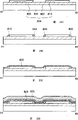
Figure 12 A to 12C representes to use the sketch map of the existing thin-film transistor of SOI substrate.Figure 12 A representes the vertical view of thin-film transistor, and Figure 12 B is equivalent to the sectional view between the dotted line O-P among Figure 12 A, and Figure 12 C is equivalent to the sectional view between the dotted line Q-R among Figure 12 A.Note, in Figure 12 A, partly omit the film of formation thin-film transistor etc.
Through using SOI substrate 9005 to form the thin-film transistor shown in Figure 12 A to 12C.In this SOI substrate 9005, layer closes and is formed with insulating barrier 9002 and silicon layer 9006 successively on support substrates 9000.Silicon layer 9006 is formed island, and sandwich gate insulation layer 9004 is formed with the conductive layer 9012 as gate electrode on this silicon layer 9006.In addition, silicon layer 9006 comprise sandwich gate insulation layer 9004 be formed on conductive layer 9012 overlapping areas in channel formation region 9008 and as the impurity range 9010 in source region or drain region.
The open 2005-019859 communique of [patent document 1] Japanese patent application
Yet, in the thin-film transistor of the use SOI of above-mentioned that kind substrate, result from the island silicon layer the end and various defectives take place.For example, under the situation of using the SOI substrate, can make the surface oxidation of silicon layer, form gate insulation layer through using thermal oxidation method.Though when utilizing thermal oxidation method, can obtain the good insulation layer, following problem is arranged: also from the end oxidation development of silicon layer, shown in the dotted line 9007 of Figure 12 B, gate insulation layer 9004 gets into the end of silicon layer and forms.
In addition, might remove the insulating barrier of the lower floor that is arranged on silicon layer owing to etching work procedure when silicon layer is formed island, utilize the influence of the washing procedure etc. of hydrofluoric acid etc.Special under the situation that makes the silicon layer filmization, its influence further obviously.At this moment, shown in the dotted line 9009 of Figure 12 C, the spreadability of gate insulation layer becomes bad easily near the end of silicon layer.
On the other hand, do not utilize thermal oxidation method to form under the situation of gate insulation layer utilizing CVD method or sputtering method, owing to step is arranged in the end of silicon layer, so the spreadability of gate insulation layer becomes bad easily in the end of silicon layer.
When in the end of silicon layer fully during the covering gate insulating barrier, silicon layer might take place and form short circuit or the leakage current between the conductive layer of gate electrode.In addition, the covering defective of gate insulation layer also becomes the main cause of the electrostatic breakdown (ESD:Electro Static Discharge) etc. of element or gate insulation layer.Particularly,, hope the filmization of gate insulation layer, and when being provided with gate insulation layer thin, the covering defective of the end of silicon layer becomes more significantly problem for low power consumption or the operating rate that improves thin-film transistor.Moreover along with the filmization of gate insulation layer, the problem of electrostatic breakdown is also further serious.
In addition, following problem is arranged also:, in the conductive layer and silicon layer overlapping areas that form gate electrode, in corner portions located (corner part) electric field takes place easily and concentrate caused leakage current especially in the end of island silicon layer.
When the problem of silicon layer end of resulting from that takes place as above-mentioned, the operating characteristic degeneration of thin-film transistor, and reliability also reduces.In addition, when making semiconductor device, rate of finished products reduces, and increases manufacturing cost.
Summary of the invention
In view of this problem and create the present invention, and its purpose be to provide a kind of semiconductor device that improves reliability and have a new construction with and manufacturing approach.The structure of semiconductor device of the present invention comprises: layer closes the SOI substrate of insulating barrier, island silicon layer successively on support substrates; Be arranged on the surface of island silicon layer and the gate insulation layer of side; Sandwich gate insulation layer and be arranged on the island silicon layer and cross the gate electrode that island silicon layer ground is provided with; Wherein, Concerning gate insulation layer, to compare with a lip-deep zone that is contacted with the island silicon layer, the dielectric constant in zone of side that is contacted with the island silicon layer is little.
In addition, other structures of semiconductor device of the present invention comprise: layer closes the SOI substrate of insulating barrier, island silicon layer successively on support substrates; Be arranged on the surface of island silicon layer and the gate insulation layer of side; Sandwich gate insulation layer and be arranged on the island silicon layer and cross the gate electrode that island silicon layer ground is provided with; Wherein, Concerning gate insulation layer; At least with the zone of gate electrode in, compare with a lip-deep zone that is contacted with the island silicon layer, the dielectric constant in zone of side that is contacted with the island silicon layer is little.
In addition, other structures of semiconductor device of the present invention comprise: layer closes the SOI substrate of insulating barrier, island silicon layer successively on support substrates; Be arranged on the surface of island silicon layer and the gate insulation layer of side; Sandwich gate insulation layer and be arranged on the island silicon layer and cross the gate electrode that island silicon layer ground is provided with; Wherein, Concerning gate insulation layer, to compare with a lip-deep zone that is contacted with the island silicon layer, the thicker and the dielectric constant in zone of side that is contacted with the island silicon layer is little.
In addition, other structures of semiconductor device of the present invention comprise: layer closes the SOI substrate of insulating barrier, island silicon layer successively on support substrates; Be arranged on the surface of island silicon layer and the gate insulation layer of side; Sandwich gate insulation layer and be arranged on the said island silicon layer and cross the gate electrode that island silicon layer ground is provided with; Wherein, Concerning gate insulation layer; At least with the zone of gate electrode in, compare with a lip-deep zone that is contacted with the island silicon layer, the thicker and the dielectric constant in zone of side that is contacted with the island silicon layer is little.
In addition, in said structure, the thickness in the zone of the side that is contacted with the island silicon layer of gate insulation layer is preferably greater than a times of a lip-deep thickness of its island silicon layer and is below three times.In other words, when a lip-deep thickness setting with the island silicon layer of gate insulation layer is t1 the and when thickness setting in the zone of the side that is contacted with the island silicon layer of gate insulation layer is t2, satisfy t1<t2≤3t1.
In addition; In said structure, be arranged on the surface of island silicon layer and the gate insulation layer of side also can be by on the surface that is contacted with the island silicon layer and second insulating barrier that first insulating barrier that is provided with is provided with being contacted with the side of island silicon layer forms.
In addition; In said structure, be arranged on the surface of island silicon layer and the gate insulation layer of side also can be formed by one that is arranged on the island silicon layer lip-deep first insulating barrier and second insulating barrier and the 3rd insulating barrier that are arranged on the side of island silicon layer.
In addition, in said structure, the bevel angle of the end of island silicon layer is preferably more than 45 degree and is lower than 95 degree.
In addition, in said structure,, both can use SIMOX (separationby implanted oxygen: inject oxygen isolate) substrate, can use again (bondedsubstrate) at the bottom of the adhesive lining as the SOI substrate.
In addition, one of manufacturing approach of semiconductor device of the present invention comprises the steps: the silicon layer of SOI substrate is formed island; Be contacted with on the surface of island silicon layer and form first insulating barrier laterally; Expose through first insulating barrier being removed selectively, form second insulating barrier of the side that is contacted with the island silicon layer to a surface of island silicon layer; The surface and the second insulating barrier ground that are contacted with the island silicon layer form the 3rd insulating barrier; Sandwich the 3rd insulating barrier and on a surface of island silicon layer, cross island silicon layer ground and form gate electrode layer.
In addition, in above-mentioned manufacturing approach, it is above and be lower than 95 degree that the bevel angle that preferably the island silicon layer is formed its end becomes 45 degree.
In addition, one of manufacturing approach of semiconductor device of the present invention comprises the steps: that silicon layer with the SOI substrate forms island and forms first silicon layer; Be contacted with a surface of first silicon layer and form first insulating barrier laterally; Expose through first insulating barrier being removed selectively, form second insulating barrier of the side that is contacted with first silicon layer, in the upper strata of first silicon layer, form amorphous area simultaneously to a surface of island first silicon layer; Remove the amorphous area that is formed in first silicon layer, form island second silicon layer; Be contacted with second silicon layer and the second insulating barrier ground and form the 3rd insulating barrier; Sandwich the 3rd insulating barrier and on a surface of second silicon layer, cross the second silicon layer ground and form gate electrode layer.
In addition, one of manufacturing approach of semiconductor device of the present invention comprises the steps: that silicon layer with the SOI substrate forms island and forms first silicon layer; Be contacted with a surface of first silicon layer and form first insulating barrier laterally; Through utilizing with the vertical direction is that the anisotropic etching of main body makes first silicon layer and first insulating layer of thin-filmization, second insulating barrier that forms island second silicon layer and be contacted with the side of second silicon layer; Be contacted with second silicon layer and the second insulating barrier ground and form the 3rd insulating barrier; Sandwich the 3rd insulating barrier and on a surface of second silicon layer, cross the second silicon layer ground and form gate electrode layer.
In addition, in above-mentioned manufacturing approach, can in its film thickness is the scope of 60nm to 70nm, form first silicon layer, and in its film thickness is the scope of 20nm to 30nm, form second silicon layer.
In addition, preferably the end of second silicon layer being formed its bevel angle, to become 45 degree above and be lower than 95 degree.
In addition, in above-mentioned manufacturing approach, second insulating barrier and the 3rd insulating barrier are formed gate insulation layer.In addition, be preferably formed its dielectric constant less than the 3rd insulating barrier the layer as second insulating barrier.
In addition, in above-mentioned manufacturing approach, also can after forming gate electrode layer, heat-treat.
In addition,, both the substrate that forms through the SIMOX method can be used, the substrate that forms through Method for bonding (wafer bonding) can be used again as the SOI substrate.
Result from the defective of end of silicon layer through being suitable for the present invention, can reducing with channel formation region.Therefore, can reduce silicon layer the end characteristic the influence that causes for semiconductor device, and the semiconductor device that improves reliability can be provided.In addition, in the manufacturing process of semiconductor device, can improve rate of finished products.
Description of drawings
Figure 1A to 1C is the figure of example that expression relates to the primary structure of semiconductor device of the present invention;
Fig. 2 A1 to 2C2 is the figure of example that expression relates to the manufacturing approach of semiconductor device of the present invention;
Fig. 3 A1 to 3C2 is the figure of example that expression relates to the manufacturing approach of semiconductor device of the present invention;
Fig. 4 A to 4C2 is the figure of example that expression relates to the manufacturing approach of semiconductor device of the present invention;
Fig. 5 A1 to 5C2 is the figure of example that expression relates to the manufacturing approach of semiconductor device of the present invention;
Fig. 6 A to 6F is the figure of example that expression relates to the manufacturing approach of semiconductor device of the present invention;
Fig. 7 A to 7C2 is the figure of example that expression relates to the manufacturing approach of semiconductor device of the present invention;
Fig. 8 A1 to 8C2 is the figure of example that expression relates to the manufacturing approach of semiconductor device of the present invention;
Fig. 9 A to 9F is the figure of example that expression relates to the manufacturing approach of semiconductor device of the present invention;
Figure 10 A to 10C2 is the figure of example that expression relates to the manufacturing approach of semiconductor device of the present invention;
Figure 11 A1 to 11C2 is the figure of example that expression relates to the manufacturing approach of semiconductor device of the present invention;
Figure 12 A to 12C is the figure of the configuration example of expression existing semiconductor devices;
Figure 13 A to 13C2 is the figure of example that expression relates to the manufacturing approach of semiconductor device of the present invention;
Figure 14 A1 to 14C2 is the figure of example that expression relates to the manufacturing approach of semiconductor device of the present invention;
Figure 15 A1 to 15B2 is the figure of example that expression relates to the manufacturing approach of semiconductor device of the present invention;
Figure 16 A to 16C is the figure that expression relates to the configuration example of semiconductor device of the present invention;
Figure 17 is the figure that expression relates to the configuration example of semiconductor device of the present invention;
Figure 18 is the figure of the configuration example of expression plasma processing apparatus;
Figure 19 A to 19C is the figure of example that expression relates to the primary structure of semiconductor device of the present invention;
Figure 20 A to 20D is the figure of example that expression relates to the manufacturing approach of semiconductor device of the present invention;
Figure 21 A to 21D is the figure of example that expression relates to the manufacturing approach of semiconductor device of the present invention;
Figure 22 A to 22C is the figure of example that expression relates to the manufacturing approach of semiconductor device of the present invention;
Figure 23 A to 23D is the figure of example that expression relates to the manufacturing approach of semiconductor device of the present invention;
Figure 24 A to 24C is the figure of example that expression relates to the manufacturing approach of semiconductor device of the present invention;
Figure 25 A to 25C is the figure of example that expression relates to the manufacturing approach of semiconductor device of the present invention;
Figure 26 A to 26E is the figure of example of the manufacturing approach of expression SOI substrate;
Figure 27 is the calcspar that expression relates to an example of semiconductor device of the present invention;
Figure 28 A to 28H is the figure of example that expression relates to the occupation mode of semiconductor device of the present invention;
Figure 29 A to 29C is vertical view and the sectional view that expression relates to an example of semiconductor device of the present invention;
Figure 30 A to 30D is the figure that explanation goes for relating to the antenna of semiconductor device of the present invention;
Figure 31 A to 31C is the figure of example of calcspar and the occupation mode of an expression example relating to semiconductor device of the present invention.
Embodiment
Below, explain with reference to accompanying drawing about execution mode of the present invention.But the present invention is not limited to following explanation, and the ordinary person of affiliated technical field can understand a fact at an easy rate, is exactly that its mode and detailed content can be transformed to various forms and not break away from aim of the present invention and scope thereof.Therefore, the present invention should not be interpreted as only for fixing in the content that the execution mode shown in following puts down in writing.Note, in the structure of the present invention of following explanation, in different accompanying drawings, use the symbol of expression same section sometimes jointly.
Figure 1A to 1C is for vertical view that the primary structure that relates to semiconductor device of the present invention is described and sectional view.Figure 1A to 1C representes the structure of thin-film transistor especially, and Figure 1A representes vertical view, and Figure 1B representes the sectional view between the dotted line O-P among Figure 1A, and Fig. 1 C representes the sectional view between the dotted line Q-R among Figure 1A.Note, in Figure 1A, partly omit film etc.
Through utilizing SOI substrate 105 to form the thin-film transistor 120 shown in Figure 1A to 1C.Thin-film transistor 120 by the silicon layer 106 of SOI substrate 105, be contacted with the side of silicon layer 106 and the insulating barrier 108 that is provided with, be arranged on the lip-deep insulating barrier of of silicon layer 106 110, this insulating barrier 110 of sandwich and the conductive layer 112 that is arranged on the silicon layer 106 constitutes.
As SOI substrate 105, use the substrate that forms through SIMOX method or Method for bonding.In this execution mode, use the substrate that on support substrates 100, is formed with insulating barrier 102, silicon layer 106 successively.
In addition, preferably form the end of silicon layer 106 to such an extent that be bordering on perpendicular shape.Specifically, with the end of silicon layer 106 form its bevel angle become 45 degree above and be lower than 95 degree, to be preferably 60 degree above and be lower than 95 degree, get final product.Form to such an extent that be bordering on perpendicular shape through end, can be reduced in the parasitic channel that the gate insulation layer as the end of silicon layer 106 in the end overlapping areas of conductive layer of gate electrode 112 and silicon layer 106 and conductive layer 112 side through being contacted with silicon layer 106 forms silicon layer 106.This is because form to such an extent that be bordering on perpendicular shape through the end with silicon layer; Follow form in end silicon layer have gentle slope bevel angle (for example; Bevel angle is below 45 degree) situation compare, can reduce the cause of the area that the end of silicon layer in the area of whole silicon layer occupies.Note, parasitic channel be meant be formed on in channel formation region with the direction that is connected source region and drain region substantially abreast the raceway groove of formation to intersect be on the direction of vertical or oblique opposite side and at the raceway groove of the end of channel formation region.Because leakage current takes place when forming parasitic channel, thus with the end of silicon layer be processed as be bordering on perpendicular shape shape to prevent that parasitic channel from being to be effective in very much the inhomogeneities of the characteristic that reduces the semiconductor device of accomplishing and to improve reliability.
In addition, bevel angle is meant that this side with layer of conical by its shape has the formed inclination angle, bottom surface of the layer of conical by its shape with this in having the layer of conical by its shape.Note, also can the end of silicon layer 106 be formed its bevel angle and be 30 degree above and be lower than 85 degree, or 45 degree above and be lower than the conical by its shape of the gentle slope of 60 degree.Can form conical by its shape through end and make its corner portions located (corner part) become gentle slope, relax electric field and concentrate on this corner portions located silicon layer 106.
Notice that in this manual, " end " of silicon layer is meant the limit part (marginal portion) of the silicon layer that forms island." side " of silicon layer is meant the face of the limit part of silicon layer.
In addition, also can in silicon layer 106, form the low concentration impurity district that distinguishes as LDD (lightly doped drain).Can form the low concentration impurity district at channel formation region with between as the impurity range in source region or drain region.In addition, with comparing as the impurity range in source region or drain region, the impurity concentration in low concentration impurity district is low.
Be formed with insulating barrier 108 with the contacts side surfaces ground of silicon layer 106.In addition, on a surface of silicon layer 106 and be formed with insulating barrier 110 on the insulating barrier 108.Insulating barrier 108 and insulating barrier 110 are as the gate insulation layer of thin-film transistor 120.In other words, relate to gate insulation layer of the present invention and do not constitute by an insulating barrier, but constitute by the compound of a plurality of insulating barriers.Notice that the border of a plurality of insulating barriers also can be for indefinite.
Can form gate insulation layer through the insulating barrier 110 that utilization is contacted with the insulating barrier 108 of the side of silicon layer 106, the surface that is contacted with silicon layer 106 and insulating barrier 108, improve spreadability at the gate insulation layer of the end of silicon layer 106.Therefore, can prevent to result from defective in the covering defective of the gate insulation layer of the end of silicon layer 106.
In addition, concerning the gate insulation layer that is formed by insulating barrier 108 and insulating barrier 110, compare with a lip-deep zone that is formed on silicon layer 106, the film thickness in zone of side that is contacted with silicon layer 106 is preferably thick.The distance setting of the most surperficial intersection point of vertical line that for example, will extend from a surface of silicon layer 106 and gate insulation layer is thickness t1.And the distance setting of the vertical line that will extend from the side of silicon layer 106 and the most surperficial intersection point of gate insulation layer is thickness t2.At this moment, gate insulation layer preferably satisfies thickness t1<thickness t2.For example, can satisfy t1<t2≤3t1.Notice that be contacted with the thickness in zone of the side of silicon layer 106, the thickness t2 of the distance of the vertical line that for example extends from the side of silicon layer 106 and the most surperficial intersection point of gate insulation layer might not be certain value.In the case, compare with thickness t1, the minimum value of thickness t2 is preferably identical with thickness t1 or greater than thickness t1.Through utilizing gate insulation layer to cover the end of silicon layer 106 fully, preferably, the thickness in the zone of the side that is contacted with silicon layer 106 is increased, can relax the electric field of the end that is applied to silicon layer 106 and prevent leakage current.
In addition, concerning the gate insulation layer that is formed by insulating barrier 108 and insulating barrier 110, compare with a lip-deep zone that is formed on silicon layer 106, the dielectric constant in zone of side that is contacted with silicon layer 106 is preferably little.For example, the dielectric constant through making insulating barrier 108 is less than insulating barrier 110, can make the dielectric constant of gate insulation layer in zone of the side that is contacted with silicon layer 106 little.Preferably, utilizing dielectric constant is that advanced low-k materials below 4 forms insulating barrier 108, gets final product.The dielectric constant in the zone through in gate insulation layer, making the side that is contacted with silicon layer 106 is less than a lip-deep zone that is contacted with silicon layer 106, can relax electric field concentrate on the end of silicon layer 106, especially in corner portions located (corner part).As a result, can prevent gate insulation layer is applied excessive electric field locally, and prevent the insulation defect of gate insulation layer.Therefore, can rate of finished products make semiconductor device well, and improve the reliability of the semiconductor device of accomplishing.
Notice that at this, what be contacted with silicon layer 106 forms insulating barrier 108 laterally with around the silicon layer 106 that forms island.In addition, we can say also that insulating barrier 108 has peristome so that the upper surface of silicon layer 106 exposes.
Note, as stated, when silicon layer is formed island, result from the various defectives of end of silicon layer easily.Especially with the end of the silicon layer of gate electrode, also defective takes place easily being formed on, and receive the influence of electrostatic breakdown etc. easily with the end of the channel formation region of the end of the silicon layer of gate electrode (channel formation region and as the boundary vicinity of the impurity range in source region or drain region).As its main cause, can enumerate as follows: the gate insulation layer of the end of channel formation region and the gate electrode side of the end (end of silicon layer) through being contacted with channel formation region in both overlapping areas forms parasitic channel easily; In channel formation region, near between wherein, compare, its end (with the boundary vicinity as the impurity range in source region or drain region) applied high voltage; When the gate electrode layer (conductive layer) that is processed to form on the upper strata, receive the influence of etching etc.; Gate insulation layer attenuation etc. locally in the end of silicon layer.Therefore,, be contacted with the insulating barrier of formation laterally of silicon layer, can reduce defectives such as insulation breakdown, electrostatic breakdown, leakage current through at least in the overlapping areas of the end of gate electrode layer and silicon layer.For example, shown in Figure 16 A to 16C,, be formed with the insulating barrier 208 of the side that is contacted with silicon layer 106, get final product in the end of the silicon layer that forms island 106 with as in conductive layer 112 overlapping areas of gate electrode.Figure 16 A representes vertical view, and Figure 16 B is equivalent to the sectional view between the dotted line O-P among Figure 16 A, and Figure 16 C is equivalent to the sectional view between the dotted line Q-R among Figure 16 A.At this, only the end overlapping areas of conductive layer 112 and silicon layer 106 with and near be formed with insulating barrier 208.Therefore, in Figure 16 B, be not formed with insulating barrier 208, and in Figure 16 C, what be contacted with silicon layer 106 is formed with insulating barrier 208 laterally in the side of silicon layer 106.
Shown in Figure 16 A to 16C,, can prevent the end of silicon layer and be used as the short circuit between the conductive layer of gate electrode through in the end overlapping areas of conductive layer that is used as gate electrode and silicon layer, forming the insulating barrier of the side that is contacted with silicon layer at least.For example, shown in figure 17, even near the insulating barrier 102 that removes the end of silicon layer 106 under silicon layer 106, also be contacted with the insulating barrier 218 of the side of silicon layer 106 through formation, can cover the end of silicon layer 106 fully.Especially, to improve the spreadability of gate insulation layer be very effective under following situation for suitable the present invention: the film thickness of gate insulation layer is in the scope of a few nm to tens nm and is thinner than the film thickness of silicon layer.In addition, through being suitable for the present invention, can relax electric field and concentrate on the end of silicon layer and prevent/reduce leakage current.Special in gate insulation layer, the dielectric constant in zone that makes the side that is contacted with silicon layer is less than a lip-deep zone that is contacted with silicon layer, can relax to apply electric field locally, and be effectively therefore.As stated, through the insulating barrier of formation laterally of the silicon layer in the end overlapping areas of the side that is contacted with silicon layer, the conductive layer that is particularly useful as gate electrode and silicon layer, can improve the reliability and the operating characteristic of the semiconductor device of completion.
Can form insulating barrier 108 and insulating barrier 110 with single layer structure or laminate structures through utilizing silica, silicon nitride, silicon oxynitride, silicon oxynitride, aluminium nitride, SiOF (fluorinated silicon oxide), SiOC (containing silicon oxide carbide), DLC (diamond-like-carbon), porous silica materials such as (porous silica).In addition, both can use same material to form insulating barrier 108 and insulating barrier 110, and can use different materials to form again.In this execution mode, use silicon oxide layer to form insulating barrier 108, and use silicon nitride layer to form insulating barrier 110.
Note, preferably through using dielectric constant to form insulating barrier 108 less than the material of insulating barrier 110.In addition, preferably wait and form insulating barrier 108 through utilizing dielectric constant to be approximately advanced low-k materials such as SiOF, SiOC, DLC, porous silica below 4.Notice that dielectric constant is that the advanced low-k materials 4 below is also referred to as the low-k material, and use low-k material and the film made is also referred to as the low-k film.So, form insulating barrier 108 through using dielectric constant less than the material of insulating barrier 110, the dielectric constant of gate insulation layer in zone that can make the side that is contacted with silicon layer is less than a lip-deep zone that is contacted with silicon layer.
Below, the manufacturing approach of the thin-film transistor 120 shown in Figure 1A to 1C is described with reference to Fig. 2 A1 to 2C2 particularly.
At first, prepare SOI substrate 105.At this, using on support substrates 100 successively, layer closes the SOI substrate 105 (with reference to Fig. 2 A1,2A2) that is formed with insulating barrier 102, silicon layer 104.
In the present invention, can use known SOI substrate, and its manufacturing approach or structure have no particular limits.As the SOI substrate, can typically enumerate at the bottom of SIMOX substrate, the adhesive lining.In addition, as the example at the bottom of the adhesive lining, can enumerate ELTRAN (registered trade mark), UNIBOND (registered trade mark) etc.
For example, concerning the SIMOX substrate, can be through monocrystalline substrate 11 being injected oxonium ions 12 and being buried oxygen (BOX heat-treating more than 1300 ℃ to form; Buried Oxide) layer 14 comes to form in its surface membrane silicon layer 16, and obtains soi structure.Through utilizing oxygen buried layer 14, membrane silicon layer 16 and monocrystalline substrate 11 insulated separation (with reference to Figure 26 A and 26B).In addition, also can use after forming oxygen buried layer, also carry out thermal oxidation be called ITOX (internal heat oxidation; Internal Thermal Oxidation) technology.
On the other hand; Concerning at the bottom of the adhesive lining; Can two monocrystalline substrate (first monocrystalline substrate 20, second monocrystalline substrate 24) be sticked together through sandwich oxidation film layer 22; And never filmization carry out in bonding monocrystalline substrate surface, comes to form from the teeth outwards membrane silicon layer 26, and obtains soi structure.Can form oxidation film layer 22 through a substrate (at this, first monocrystalline substrate 20) is carried out thermal oxidation.In addition, can directly two monocrystalline substrate be sticked together and do not utilize adhesive.For example; Can through first monocrystalline substrate 20 is heat-treated form oxidation film layer 22 after; Make it and second monocrystalline substrate 24 overlapping; And more than 800 ℃, be preferably about 1100 ℃ and heat-treat, and be utilized in the chemical bond of adhesive interface, two substrates are sticked together.Then, can grind second monocrystalline substrate 24, form membrane silicon layer 26 (with reference to Figure 26 C, 26D, 26E) with desirable thickness through never bonding surface one side.In addition, also can use the technology that is called smart peeling (Smart-Cut, registered trade mark) method.This technology is following: after bonding, second monocrystalline substrate 24 is not ground; Form slight void and in the zone of the prescribed depth of second monocrystalline substrate 24, inject hydrogen ion, and utilize the growth of caused this slight void of the heat treatment substrate of riving.In addition, after second monocrystalline substrate is ground, also can use to be called PACE (plasma auxiliary chemical etching; Plasma Assisted ChemicalEtching) technology.This technology is following: utilize small-sized plasma-etching apparatus in the control of carrying out locality, substrate to be carried out etching, and realize filmization.
In the SOI substrate 105 shown in this execution mode, support substrates 100 is equivalent to the monocrystalline substrate shown in Figure 26 A to 26E, and insulating barrier 102 is equivalent to oxygen buried layer or oxidation film layer, and silicon layer 104 is equivalent to be formed on lip-deep membrane silicon layer.
Then, etch silicon layer 104 selectively, form island silicon layer 106 (with reference to Fig. 2 B1,2B2).At this moment, both can silicon layer 106 be formed its end becomes perpendicular shape, and can silicon layer 106 be formed its end again becomes conical by its shape.Through changing etching condition etc., can suitably select the shape of the end of silicon layer 106.Preferably with the end of silicon layer 106 form its bevel angle become 45 degree above and be lower than 95 degree, more preferably 60 degree are above and be lower than 95 degree, get final product.Form to such an extent that be bordering on perpendicular shape through end, can reduce parasitic channel silicon layer 106.
Then, covering silicon layer 106 ground formation insulating barrier 107 (below, be also referred to as first insulating barrier 107) (with reference to Fig. 2 C1 and 2C2).Through utilizing CVD method or sputtering method and using silica, silicon nitride, silicon oxynitride, silicon oxynitride, SiOF, SiOC, DLC, porous silica materials such as (poroussilica), form first insulating barrier 107.
Form first insulating barrier 107 with the film thickness that can cover the end of silicon layer 106 fully.Be to be formed in 1.5 times to 3 times the scope of film thickness of silicon layer 106 of lower floor to form first insulating barrier 107 preferably at its film thickness.
Then, be anisotropic etching and the etching selectively of main body through first insulating barrier 107 is carried out with the vertical direction, form the insulating barrier 108 (below, be also referred to as second insulating barrier 108) (with reference to Fig. 3 A1 and 3A2) of the side that is contacted with silicon layer 106.
When first insulating barrier 107 being carried out be the anisotropic etching of main body with the vertical direction, from a surface that is formed on silicon layer 106 and first insulating barrier 107 on the insulating barrier 102 be etched gradually.Note, form first insulating barrier 107 on a surface of silicon layer 106 and on the insulating barrier 102 with roughly the same film thickness.Therefore, through when expose on a surface of silicon layer 106, stopping etching, can be only the zone of the side that is contacted with silicon layer 106 with and near stay first insulating barrier 107.First insulating barrier 107 that stays is equivalent to second insulating barrier 108.Note, form to such an extent that be bordering on perpendicular shape through end with silicon layer 106, can be easily the zone of the side that is contacted with silicon layer 106 with and near stay first insulating barrier 107.In other words, can form second insulating barrier 108 easily.
So long as can to carry out with the vertical direction being the anisotropic etching of main body, just to the not special restriction of the engraving method of first insulating barrier 107.For example, can utilize reactive ion etching (RIE:Reactive Ion Etching).In addition, according to the plasma genetic method, reactive ion etching is classified as parallel flat mode, magnetic control mode, 2 frequency modes (dual-frequency type), ECR mode, helicon (helicon) mode, ICP mode etc.As the etching gas that use this moment, be chosen in and can obtain high etching selectivity between first insulating barrier 107 and the layer in addition (silicon layer 106), get final product.When etching isolation layer selectively, for example can use CHF
3, CF
4, C
4F
8, C
2F
6, NF
3Deng fluorine type gas.In addition, also can suitably append inert gas or O such as He, Ar, Xe
2Gas, H
2Gas.
Through suitably selecting to be used for film forming material, etching condition etc., can change the shape of second insulating barrier 108.In this execution mode, it is consistent substantially with silicon layer 106 that second insulating barrier 108 is formed its height towards vertical direction that (is contacted with the face of insulating barrier 102) from the bottom surface.In addition, the face with the side that is not contacted with silicon layer 106 of second insulating barrier 108 forms bending.Specifically, it is formed have any curvature and be convex form for the edgewise bend of silicon layer 106 of contact.Certainly, the not special restriction of the present invention also can form the shape with angle with second insulating barrier 108, rather than bending.Preferably, when the corner portions located with second insulating barrier 108 forms the shape of gentle slope, can make the spreadability of the layer (at this, insulating barrier 110) that is laminated in the upper strata good.Notice that etching condition also is meant pressure in the amount of power that is applied to the electrode that substrate is housed, the electrode temperature that the electrode of substrate is housed, the reative cell etc. except the flow rate ratio of the kind that is meant etching gas, all gases.
Then, forming insulating barrier 110 (below, be also referred to as the 3rd insulating barrier 110) (with reference to Fig. 3 B1 and 3B2) on the silicon layer 106 and second insulating barrier 108.Through utilizing CVD method or sputtering method and using materials such as silica, silicon nitride, silicon oxynitride, silicon oxynitride, aluminium nitride, form the 3rd insulating barrier 110.In addition, through using in these materials one or more to form the 3rd insulating barrier 110 with single layer structure or laminate structures.Be 1nm to 50nm at its film thickness, be preferably 1nm to 20nm, more preferably form the 3rd insulating barrier 110 in the scope of 1nm to 10nm.In this execution mode, form silicon oxynitride layer as the 3rd insulating barrier 110 with the film thickness of 20nm.
In addition, also can use the phase oxidative or the solid phase nitrogenize that utilize Cement Composite Treated by Plasma to form the 3rd insulating barrier 110.For example, can make silicon layer 106 and 108 oxidations of second insulating barrier or nitrogenize, form the 3rd insulating barrier 110 through utilizing Cement Composite Treated by Plasma.
Concerning the phase oxidative that utilizes Cement Composite Treated by Plasma handle or the solid phase nitrogen treatment, preferably utilize following plasma and carry out: utilize microwave high frequency waves such as (being typically 2.45GHz) to excite, and its electron density is 1 * 10
11Cm
-3More than and 1 * 10
13Cm
-3Below, and its electron temperature is more than the 0.5eV and below the 1.5eV.This be because for handle at phase oxidative or the solid phase nitrogen treatment in, under the temperature below 500 ℃, form the cause that obtains practical reaction speed in the careful insulating barrier.
Under the situation of the surface oxidation that makes the silicon layer 106 and second insulating barrier 108 through Cement Composite Treated by Plasma, in the oxygen containing atmosphere of bag, (for example, comprising oxygen (O
2), ozone (O
3), nitrous oxide (N
2O), nitric oxide (NO) or nitrogen dioxide (NO
2) and the atmosphere of rare gas (contain in helium (He), neon (Ne), argon (Ar), krypton (Kr), the xenon (Xe) at least a) in; Perhaps, comprising oxygen (O
2), ozone (O
3), nitrous oxide (N
2O), nitric oxide (NO) or nitrogen dioxide (NO
2), hydrogen (H
2) and the atmosphere of rare gas in) carry out.In addition, under the surfaces nitrided situation that makes silicon layer 106 and insulating barrier 108 through Cement Composite Treated by Plasma, in the bag nitrogen-containing atmosphere, (for example, comprising nitrogen (N
2) and the atmosphere of rare gas (comprise among He, Ne, Ar, Kr, the Xe at least a) in; In the atmosphere that comprises nitrogen, hydrogen and rare gas; Perhaps, comprising NH
3In the atmosphere of rare gas) carry out Cement Composite Treated by Plasma.As rare gas, for example preferably use Ar.In addition, also can use the mist of Ar and Kr.
At this, Figure 18 illustrates the configuration example of the plasma processing apparatus 1080 that is used to carry out Cement Composite Treated by Plasma.This plasma processing unit 1080 comprises: brace table 1088; Be used for the gas supply section 1084 of supply gas; Be connected to the exhaust outlet 1086 of vacuum pump in order to get rid of gas; Antenna 1098; Dielectric plate 1082; And input is used to produce the high frequency waves supply section 1092 of the high frequency waves of plasma.Utilize brace table 1088 to keep handled object 1010.In addition, be set to brace table 1088, also can control the temperature of handled object 1010 through temperature control part being divided 1090.Handled object 1010 is carried out the matrix of Cement Composite Treated by Plasma, and in this execution mode, it is equivalent on support substrates 100, be formed with successively the lamilated body of insulating barrier 102, island silicon layer 106.
Below, the object lesson that uses plasma processing apparatus 1080 shown in Figure 180 on the surface of silicon layer, to form insulating barrier is described.Notice that Cement Composite Treated by Plasma will be included in its category oxidation processes, nitrogen treatment, oxynitriding processing, hydrogenation treatment, the surface modification treatment that substrate, silicon layer, insulating barrier, conductive layer carry out.In these are handled, select to get final product from the gas of gas supply section 1084 supplies according to its purpose.
At first, make in the process chamber of plasma processing apparatus shown in Figure 180 1080 and become vacuum.Then, from gas supply section 1084 supply rare gas, comprise the gas of oxygen or nitrogen.In room temperature or utilize temperature control part to divide 1090 and the heating handled object 1010 more than 100 ℃ and in the temperature range below 550 ℃ that obtains.Interval between handled object 1010 and the dielectric plate 1082 (below, be also referred to as electrode gap) be 20mm above and (be preferably 20mm above and below the 60mm) below the 200mm about.
Then, from high frequency waves supply section 1092 high frequency waves are input to antenna 1098.At this, input microwave (frequency is 2.45GHz) is as high frequency waves.And,, produce plasma 1094, and, produce oxygen base (also comprising the OH yl sometimes) or nitrogen base (also comprising the NH yl sometimes) through utilizing this plasma 1094 through through dielectric plate 1082 microwave being input in the process chamber from antenna 1098.At this moment, through the gas that utilization is supplied, produce plasma 1094.
When through the input microwave when producing plasma 1094, can produce low electron temperature (below the 3eV, be preferably below the 1.5eV) and high electron density (1 * 10
11Cm
-3More than) plasma.Specifically, preferably producing electron temperature is more than the 0.5eV and below the 1.5eV, and electron density is 1 * 10
11Cm
-3More than and 1 * 10
13Cm
-3Following plasma.Notice that in this manual, the low electron temperature that produces through the input microwave and the plasma of high electron density are also referred to as high-density plasma.In addition, utilize high-density plasma and carry out Cement Composite Treated by Plasma and be also referred to as high-density plasma and handle.
, make the surface oxidation that is formed on the silicon layer in the handled object 1010 or nitrogenize and form insulating barrier because oxygen base (also comprising the OH yl sometimes) or nitrogen base (also comprising the NH yl sometimes) that plasma 1094 produces through utilizing.At this moment, when in the gas that rare gas such as argon is blended in supply, can utilize the kind that excites of rare gas to produce oxygen base or nitrogen base efficiently.Note,, in the insulating barrier that forms, contain rare gas sometimes using under the situation of rare gas as supply gas.Through using the activation base that utilizes plasma to excite effectively, can under the low temperature below 500 ℃, utilize oxidation, the nitrogenize of solid phase reaction.
An example of the 3rd desirable insulating barrier 110 that forms as utilizing the high-density plasma that uses device shown in Figure 180 to handle; Cement Composite Treated by Plasma thickness with 3nm to 6nm on a surface of silicon layer 106 through being utilized in the oxygen containing atmosphere of bag forms silicon oxide layer; In the bag nitrogen-containing atmosphere, carry out nitridation plasma then and handle, form the nitrogen plasma treatment layer for the surface of this silicon oxide layer.Specifically, at first through in the oxygen containing atmosphere of bag, carrying out Cement Composite Treated by Plasma, the thickness with 3nm to 6nm on a surface of silicon layer 106 forms silicon oxide layer.Then, through continuing in the bag nitrogen-containing atmosphere, to carry out Cement Composite Treated by Plasma, the high nitrogen plasma treatment layer of nitrogen concentration is set at surface or its near surface of silicon oxide layer.Notice that near surface is meant in the degree of depth from the scope of the surperficial nearly 0.5nm to 1.5nm of silicon oxide layer.For example, through in the bag nitrogen-containing atmosphere, carrying out Cement Composite Treated by Plasma, obtain in the structure that contains nitrogen from the surface of silicon oxide layer towards the degree of depth of the nearly 1nm of vertical direction with the ratio of 20 atom % to 50 atom %.In addition, can utilize high-density plasma to handle surface oxidation or the nitrogenize that also makes insulating barrier 108, insulating barrier 102.
For example, can make surface oxidation, form the careful oxide layer that does not have interface deformation through utilizing Cement Composite Treated by Plasma into the silicon layer 106 of monocrystalline silicon.In addition, when through utilizing Cement Composite Treated by Plasma to make this oxide layer nitrogenize, when the oxygen that makes nitrogen be substituted in its skin section forms nitration case, can further realize carefulization.Thus, can form the high insulating barrier of dielectric voltage withstand.
In a word, handle or the solid phase nitrogen treatment the equal insulating barrier of heat oxide film that can obtain Yu in 950 ℃ to 1050 ℃ scope, form through the phase oxidative that utilizes Cement Composite Treated by Plasma that uses above-mentioned that kind.In other words, can form the insulating barrier of the high insulating barrier of reliability as the gate insulating film that is used as semiconductor element, particularly thin-film transistor or non-volatile memory device.
Then, sandwich the 3rd insulating barrier 110 forms the conductive layer 112 (with reference to Fig. 3 C1,3C2) as gate electrode on silicon layer 106.Can be through using tantalum (Ta), tungsten (W), titanium (Ti), molybdenum (Mo), chromium (Cr), aluminium (Al), copper (Cu) or niobium (Nb) metallic element of etc.ing, perhaps comprising and the alloy material or the compound-material of this metallic element form conductive layer 112.In addition, can use also that to give the polysilicon of the impurity element of a conductivity type be typical semi-conducting material to be added with phosphorus etc., form conductive layer 112.Can through use these materials and utilize the CVD method or sputtering method on whole surface, form conductive layer 112 after this conductive layer 112 of etching selectively, it is processed as desirable shape.In addition, conductive layer 112 can be single layer structure or laminate structures.Be 100nm to 1000nm at its film thickness, be preferably 200nm to 800nm, more preferably form conductive layer 112 in the scope of 300nm to 500nm.
Then, through silicon layer 106 is added the impurity element of giving a conductivity type selectively, form channel formation region 114, as the impurity range 116 in source region or drain region.At this, as mask, add the impurity element of giving a conductivity type with conductive layer 112.As the impurity element of giving a conductivity type, can use boron (B), aluminium (Al), gallium (Ga) etc. to give the element that element and the phosphorus (P) of p type, arsenic (As) etc. are given the n type.
Note, preferably,, the impurity element of interpolation is activated through after silicon layer 106 is added the impurity element of giving a conductivity type, heat-treating.Can be through illuminating laser beam, or use RTA or annealing furnace, heat-treat.Specifically, 400 ℃ to 700 ℃, be preferably in 500 ℃ to 550 ℃ the temperature range and heat-treat, get final product.In addition, preferably in blanket of nitrogen, heat-treat.For example, can realize activating through the heating of carrying out four hours at 550 ℃.In addition, when forming second insulating barrier 108 when etching first insulating barrier 107 selectively sometimes, since etching condition, the material that is used for forming each film or film thickness etc., a part of amorphization of silicon layer 106.In the case, through heat-treating, except realizing activation, can also realize the crystallization again of silicon layer.
With above-mentioned operation, can form and be suitable for the thin-film transistor 120 that the present invention forms.Notice that the structure of the TFT shown in this execution mode is an example, and is not limited to illustrated structure.For example, also can adopt multi-gate structure, it comprises: the silicon layer with the plural at least channel formation region that is connected in series; And the plural at least gate electrode layer that each channel formation region is applied electric field.In addition, also can in the silicon layer of TFT, form the LDD district.
In addition, though forming the example of individual layer conductive layer shown in this execution mode, the not special restriction of the present invention as gate electrode.Both can the side of gate electrode be formed conical by its shape, can gate electrode be formed the laminate structures that is made up of two-layer above conductive layer again.In addition, also can gate electrode be formed the laminate structures that is made up of two conductive layers and make the angle of taper of each layer different.In addition, also can be contacted with and form the insulating barrier that is also referred to as sidewall laterally as the conductive layer of gate electrode.
During the thin-film transistor made when use being suitable for the present invention, can reduce resulting from the defective of end of island silicon layer.Therefore, can the high semiconductor device of fabrication reliability.In addition, also can make semiconductor device with the good mode of rate of finished products.
Note, can this execution mode and other execution modes shown in this specification suitably be made up.
In this execution mode, explanation utilizes the example of making semiconductor device with above-mentioned execution mode 1 different manufacturing approach with reference to Fig. 4 A to Fig. 6 F.
Fig. 4 A is the vertical view that is used for explaining the primary structure that relates to semiconductor device of the present invention.Note, in Fig. 4 A, partly omit film etc.
In the semiconductor device shown in Fig. 4 A, use the SOI substrate to be formed with thin-film transistor.The surface silicon layer of SOI substrate is formed island, and crosses the conductive layer 314 that island silicon layer 313 ground are provided with the formation gate electrode.What in addition, be contacted with island silicon layer 313 is provided with insulating barrier 310 laterally.Though this illustrate around the entire circumference of island silicon layer 313 the example of insulating barrier 310 is set, the insulating barrier of the side that is contacted with island silicon layer 313 is set in conductive layer 314 and silicon layer 313 overlapping areas at least, get final product.Certainly, also can be in conductive layer 314 and silicon layer 313 overlapping areas with and near setting be contacted with the insulating barrier of the side of island silicon layer 313.
In silicon layer 313, be formed with channel formation region, as a pair of low concentration impurity district 317 in LDD district, be used as a pair of high concentration impurities district 318 in source region or drain region.With the consistent substantially zone of conductive layer 314 in silicon layer 313 in be formed with channel formation region, it is between a pair of high concentration impurities district 318.In addition, between channel formation region and high concentration impurities district 318, be formed with low concentration impurity district 317.
Then, the manufacturing approach of the semiconductor device shown in the key diagram 4A.At this, with reference to sectional view between the dotted line O-P among Fig. 4 A and the sectional view between the dotted line Q-R, explanation particularly.
At first, preparing on support substrates 300 successively, layer closes the SOI substrate 305 (with reference to Fig. 4 B1,4B2) that is formed with insulating barrier 302, first silicon layer 306.Then, cover first silicon layer, 306 ground and form first insulating barrier 308 (with reference to Fig. 4 C1,4C2).Note because up to the operation that forms first insulating barrier 308 according to the SOI substrate 105 shown in the above-mentioned execution mode 1, the explanation of insulating barrier 107, explain so simplify.
As SOI substrate 305, known SOI substrate such as can use at the bottom of SIMOX substrate, the adhesive lining.Through the surface of etching SOI substrate 305 selectively, form island first silicon layer 306.Be 10nm to 150nm at its film thickness, be preferably in the scope of 30nm to 100nm or 10nm to 30nm and form first silicon layer 306, get final product.In addition, both can the end of first silicon layer 306 be formed perpendicular shape, can the end of first silicon layer 306 be formed conical by its shape again.In this execution mode, with the end of first silicon layer 306 form its bevel angle become 45 degree above and be lower than 95 degree, to be preferably 60 degree that are bordering on perpendicular shape above and be lower than 95 degree.Precipitous through becoming in the taper of the end of first silicon layer 306, the parasitic channel of the semiconductor device of accomplishing after can reducing.Notice that the present invention has no particular limits.Also can the end of first silicon layer 306 be formed its bevel angle become 30 degree above and be lower than 85 degree, or 45 degree above and be lower than the conical by its shape of the gentle slope of 60 degree.
Through utilizing CVD method or sputtering method and using silica, silicon nitride, silicon oxynitride, silicon oxynitride, aluminium nitride, SiOF, SiOC, DLC, porous silica materials such as (porous silica), form first insulating barrier 308.In addition, form first insulating barrier 308 with the film thickness that can cover the end of first silicon layer 306 at least fully.Preferably first insulating barrier 308 is formed its film thickness and become 1.5 times to 3 times of first silicon layer 306.
In addition, preferably use its dielectric constant to form first insulating barrier 308 less than the material of a lip-deep insulating barrier 312 that is formed on silicon layer later on.In the semiconductor device of accomplishing afterwards, first insulating barrier 308 forms the gate insulation layer in the zone of the side that is contacted with silicon layer.When silicon layer was formed island, electric field concentrated on the end of silicon layer easily, especially in corner portions located (corner part).When electric field concentrated on the end of silicon layer, the insulation defect such as insulation breakdown or leakage current of gate insulation layer took place easily.Therefore; Through using its dielectric constant to form first insulating barrier 308 of the side that is contacted with silicon layer less than the material of a lip-deep insulating barrier that is formed on silicon layer later on; Can prevent gate insulation layer is applied excessive electric field equal pressure locally, so be preferred.
Then, be anisotropic etching and etching first insulating barrier 308 selectively of main body through carrying out with the vertical direction, form second insulating barrier 310 of the side that is contacted with first silicon layer 306.At this moment, the upper layer part amorphization of first silicon layer 306 and form amorphous tagma 311 (with reference to Fig. 5 A1,5A2).
For example, form silicon oxynitride layer as first insulating barrier 308.Insulating barrier 302 is set at silicon oxide layer, and first silicon layer 306 is set at monocrystalline silicon layer.Then, be that the anisotropic dry etch of main body comes etching first insulating barrier 308 through utilizing with the vertical direction.From a surface that is formed on first silicon layer 306 and lip-deep first insulating barrier 308 of insulating barrier 302 carry out etching.Note, on a surface of first silicon layer 306 and on the insulating barrier 302, be formed with first insulating barrier 308 with roughly the same film thickness.Therefore, through when expose on a surface of first silicon layer 306, stopping etching, can be only the zone of the side that is contacted with first silicon layer 306 with and near stay first insulating barrier 308.First insulating barrier 308 that stays is equivalent to second insulating barrier 310.Note, when forming to such an extent that be bordering on perpendicular shape through end with first silicon layer 306, can be only the zone of the side that is contacted with first silicon layer 306 with and near easy formation second insulating barrier 310.In addition, in this execution mode, it is consistent substantially with first silicon layer 306 that second insulating barrier 310 is formed its height towards vertical direction that (is contacted with the face of insulating barrier 302) from the bottom surface.In addition, the face that second insulating barrier 310 is formed its side that is not contacted with first silicon layer 306 is a convex form with respect to the edgewise bend of first silicon layer 306.Certainly, the present invention has no particular limits, and also can second insulating barrier 310 be formed the shape with angle, rather than bending.Preferably, when the corner portions located with second insulating barrier 310 forms the shape of gentle slope, can make the spreadability of the layer (at this, insulating barrier 312) that is laminated in the upper strata good.
So long as can to carry out with the vertical direction being the anisotropic etching of main body, just the engraving method to first insulating barrier 308 has no particular limits.For example, can use reactive ion etching such as parallel flat mode, magnetic control mode, 2 frequency modes, ECR mode, helicon (helicon) mode, ICP mode etc.As etching gas, be chosen in and can obtain high etching selectivity between first insulating barrier 308 and the layer in addition (first silicon layer 306), get final product.For example, through using CHF
3, CF
4, C
4F
8, C
2F
6, NF
3Deng fluorine type gas, etching isolation layer selectively.In addition, also can suitably append inert gas or O such as He, Ar, Xe
2Gas, H
2Gas.Note,, can control the shape of second insulating barrier 310 through suitably changing etching condition.In this execution mode, through reactive ion etching and the use CHF that utilizes the ICP mode
3Gas and He gas carry out the etching for first insulating barrier 308 as etching gas.
When first insulating barrier 308 was carried out anisotropic dry etch, because the influence of the energy of plasma etc., the upper layer part amorphization of first silicon layer 306 formed amorphous tagma 311.Through the film thickness of controlling first silicon layer 306, the material that is used for forming first insulating barrier 308, or the etching condition of first insulating barrier 308 etc., form amorphous tagma 311.Amorphous tagma 311 is formed its film thickness to be become 0.2 to 0.6 times of first silicon layer 306, is preferably about 0.3 to 0.5 times.Note, form amorphous tagma 311 in the direction that from a surface of first silicon layer 306, (is contacted with the face of insulating barrier 302) towards the bottom surface.
Then, be formed on the amorphous tagma 311 of the upper layer part of first silicon layer 306, form second silicon layer 313 through etching selectively.Then, cover second insulating barrier 310 and second silicon layer, 313 ground form the 3rd insulating barrier 312 (with reference to Fig. 5 B1,5B2).
Be formed on the amorphous tagma 311 of the upper layer part of first silicon layer 306 through etching selectively, form second silicon layer 313.First silicon layer 306 is a monocrystalline silicon, and when forming second insulating barrier 310 when etching first insulating barrier 308, the upper layer part of first silicon layer 306 is formed amorphous silicon layer by decrystallized.The amorphous silicon layer that form this moment is equivalent to the amorphous tagma 311 of this execution mode.Therefore, stay monocrystalline silicon layer as second silicon layer 313 through etching selectively as the amorphous silicon layer in amorphous tagma 311.Note, the bevel angle that second silicon layer 313 is formed its end become 45 degree above and be lower than 95 degree, more preferably to be bordering on perpendicular shape 60 degree above and be lower than 95 degree, get final product.In addition, second insulating barrier 310 that forms laterally that is contacted with first silicon layer 306 also stays etching method for amorphous tagma 311 after always, and becomes to give prominence to respect to second silicon layer 313 and be the state of convex.
As the engraving method in amorphous tagma 311,, just have no particular limits so long as can obtain the high etching selectivity of amorphous tagma 311 and other insulating barriers (for example, second insulating barrier 310, insulating barrier 302).Note, because the etching selectivity of amorphous silicon layer and monocrystalline silicon layer is low, thus form with the film thickness of controlling amorphous tagma 311 to a certain degree in advance, and to vertical direction first silicon layer 306 is etched into and can infer the degree of depth that is formed with amorphous tagma 311.As engraving method, for example can use reactive ion etchings such as parallel flat mode, magnetic control mode, 2 frequency modes, ECR mode, helicon (helicon) mode, ICP mode.As the etching gas that use this moment, be chosen in and can obtain high etching selectivity between amorphous tagma 311 and other insulating barriers, get final product.For example, can use Cl
2Deng chlorine class gas or HBr gas.In addition, also can use HBr gas and Cl
2The mist of gas.In addition, also can suitably append inert gases such as He, Ar.In this execution mode, through using Cl
2Gas comes etching method for amorphous tagma 311 selectively as etching gas.
Through utilizing CVD method or sputtering method and using materials such as silica, silicon nitride, silicon oxynitride, silicon oxynitride, aluminium nitride, form the 3rd insulating barrier 312.Through using in these materials one or more, form the 3rd insulating barrier 312 with single layer structure or laminate structures.In addition, also can form the 3rd insulating barrier 312 through using such second silicon layer 313 that utilizes that high-density plasma handles shown in the execution mode 1, or the phase oxidative or the solid phase nitrogenize of second silicon layer 313 and second insulating barrier 310.Be 1nm to 50nm at its film thickness, be preferably 1nm to 20nm, more preferably in the scope of 1nm to 10nm, form the 3rd insulating barrier 312.
Second insulating barrier 310 and the insulating barrier 312 that form through above operation are used as gate insulation layer.In other words, relate to gate insulation layer of the present invention and do not constitute by an insulating barrier, but constitute by the compound of a plurality of insulating barriers.So, be contacted with second insulating barrier 310 of the side of silicon layer through formation, can make the spreadability of gate insulation layer good in the end of silicon layer.For example; Even because the perhaps washing of the use hydrofluoric acid that brings of various operation etc. of etching when silicon layer is processed as island; Remove under the end of silicon layer with and near the situation of insulating barrier (insulating barrier on the support substrates) under, also can cover silicon layer fully.Therefore, can prevent to result from generation, electrostatic breakdown etc. at the silicon layer of the covering defective of the gate insulation layer of the end of silicon layer and the short circuit between the gate electrode layer, leakage current.
Notice that concerning the gate insulation layer that is made up of second insulating barrier 310 and the 3rd insulating barrier 312, the film thickness in zone that is contacted with the side of second silicon layer 313 preferably is thicker than a lip-deep zone that is formed on second silicon layer 313.The distance setting of the most surperficial intersection point of vertical line that for example, will extend from a surface of second silicon layer 313 and gate insulation layer is thickness t1.And the distance setting of the vertical line that will extend from the side of second silicon layer 313 and the most surperficial intersection point of gate insulation layer is thickness t2.Gate insulation layer preferably satisfies thickness t1<thickness t2.The thickness in zone that is contacted with the side of second silicon layer 313 is not a certain value.But, in the case, to compare with thickness t1, the minimum value of thickness t2 is preferably identical with thickness t1 or greater than thickness t1.So, can utilize gate insulation layer to come to cover fully the end of silicon layer.
In addition, concerning the gate insulation layer that is made up of second insulating barrier 310 and the 3rd insulating barrier 312, the dielectric constant in zone of side that is contacted with second silicon layer 313 is preferably less than a lip-deep zone that is formed on second silicon layer 313.For example, the dielectric constant through making second insulating barrier 310 is less than the 3rd insulating barrier 312, can make the dielectric constant of gate insulation layer in zone of the side that is contacted with second silicon layer 313 little.Preferably, be that advanced low-k materials below 4 forms second insulating barrier 310 through utilizing dielectric constant, get final product.The dielectric constant in the zone through in gate insulation layer, making the side that is contacted with silicon layer can prevent that electric field from concentrating on the end of silicon layer, and can reduce the insulation defect of gate insulation layer less than a lip-deep zone that is contacted with silicon layer, is preferred therefore.
Then, sandwich the 3rd insulating barrier 312 forms the conductive layer 314 as gate electrode on second silicon layer 313.With conductive layer 314 is that mask adds the impurity element of giving a conductivity type to second silicon layer 313.The impurity range that is formed on this moment in second silicon layer 313 constitutes the part in the LDD district of formation later on.
Then, form the insulating barrier 315 of the side that is contacted with conductive layer 314.Then; With insulating barrier 315 and conductive layer 314 is mask; Add the impurity element give a conductivity type, form channel formation region 316, as the low concentration impurity district 317 in LDD district, be used as the high concentration impurities district 318 (with reference to Fig. 5 C1,5C2) in source region or drain region.
Can form conductive layer 314 through using tantalum (Ta), tungsten (W), titanium (Ti), molybdenum (Mo), chromium (Cr), aluminium (Al), copper (Cu) or niobium (Nb) metallic element of etc.ing, perhaps comprising the alloy material or the compound-material of this metallic element.In addition, also can to give the polysilicon of the impurity element of a conductivity type be typical semi-conducting material to be added with phosphorus etc. through using, form conductive layer 314.Through using these materials and utilize the CVD method or sputtering method forms after the conductive layer 314 on whole surface, this conductive layer of etching 314 is processed as desirable shape with it selectively, gets final product.In addition, form conductive layer 314, get final product with single layer structure or laminate structures.Be 100nm to 1000nm at its film thickness, be preferably 200nm to 800nm, more preferably form conductive layer 314 in the scope of 300nm to 500nm.
Concerning insulating barrier 315, through utilizing CVD method or sputtering method and using organic materials such as inorganic material, organic resin such as silica, silicon nitride, silicon oxynitride, silicon oxynitride to form insulating barrier with single layer structure or laminate structures.And, be anisotropic etching and this insulating barrier of etching selectively of main body through utilizing with the vertical direction, can form the insulating barrier 315 of the side that is contacted with conductive layer 314.Insulating barrier 315 is also referred to as sidewall.At this, the face of the side that is not contacted with conductive layer 314 of insulating barrier 315 is formed bending.Specifically, it is formed have any curvature and be convex form with respect to the edgewise bend of conductive layer 314 of contact.Certainly, the present invention has no particular limits, and also can insulating barrier 315 be formed the shape with angle, rather than bending.Notice that insulating barrier 315 is also used mask as the doping when forming the LDD district.
In second silicon layer 313, be formed with channel formation region 316, low concentration impurity district 317, high concentration impurities district 318.Sandwich the 3rd insulating barrier 312 with the consistent substantially zone of conductive layer 314 in form channel formation region 316.Sandwich the 3rd insulating barrier 312 with the consistent substantially zone of insulating barrier 315 in and between high concentration impurities district 318 and channel formation region 316, form low concentration impurity district 317.Note, low concentration impurity district 317 might not be set.
In high concentration impurities district 318 to be added with impurity element than low concentration impurity district's 317 higher concentration.As the impurity element of giving a conductivity type, can use phosphorus (P) or arsenic (As) etc. to give the impurity element that the impurity element of n type, boron (B), aluminium (Al) or gallium (Ga) etc. are given the p type.
Through above-mentioned operation, can form and be suitable for the thin-film transistor 320 that the present invention forms.
In addition, through after second silicon layer 313 is added the impurity element of giving a conductivity type, heat-treating, the impurity element of interpolation is activated.Can be through illuminating laser beam, or use RTA or annealing furnace, heat-treat.Specifically, 400 ℃ to 700 ℃, be preferably in 500 ℃ to 550 ℃ the temperature range and heat-treat, get final product.In addition, preferably in blanket of nitrogen, heat-treat.For example, can realize activating through the heating of carrying out four hours at 550 ℃.In addition, have under the situation in amorphous tagma,, except the activation that realizes impurity element, can also realize the crystallization again of silicon layer through heat-treating in the part of second silicon layer 313.
In addition, also can make TFT through using the manufacturing approach shown in Fig. 6 A to 6C or Fig. 6 D to 6F.Note, use on support substrates 300 successively that layer closes the SOI substrate 305 that is formed with insulating barrier 302, island first silicon layer 306, and identical up to the method that on this silicon layer 306, forms first insulating barrier 308 and Fig. 4 B1,4C1, therefore omission explanation.
At first, the manufacturing approach shown in the key diagram 6A to 6C.On first silicon layer 306, form (with reference to Fig. 4 C1) after first insulating barrier 308, carrying out with the vertical direction is anisotropic etching and etching first insulating barrier 308 selectively of main body, forms second insulating barrier 330 of the side that is contacted with silicon layer 306.The upper layer part of first silicon layer 306 is formed amorphous tagma 331 (with reference to Fig. 6 A) by amorphization.At this moment, the control etching condition so that be contacted with first silicon layer 306 the side second insulating barrier 330 (face that contacts with insulating barrier 302) is lower than first silicon layer 306 towards the height of vertical direction from the bottom surface.Preferably, make as one man forming substantially of second insulating barrier 330, get final product from the bottom surface towards the height of vertical direction and the height from the bottom surface to amorphous tagma 331 of first silicon layer 306.
Can second insulating barrier 330 be processed as desirable shape through the etching condition such as gaseous species and gas flow ratio that change is used for etching gas.For example; Etching selectivity through improving first insulating barrier 308 and other layers (first silicon layer 306) and making selectively for the etching of first insulating barrier 308 carries out, and what can make second insulating barrier 330 is lower than first silicon layer 306 from the bottom surface towards the height of vertical direction.In other words, noncrystal district 331 is not contacted with second insulating barrier 330.
Then, be formed on the amorphous tagma 331 of the upper layer part of first silicon layer 306, form second silicon layer 332 (with reference to Fig. 6 B) through etching selectively.Note; Because amorphous tagma 331 and be that the etching selectivity of first silicon layer 306 of monocrystalline silicon layer is low; So, and to vertical direction first silicon layer 306 is etched into and to infer the degree of depth that is formed with amorphous tagma 311 in advance controlling the film thickness in amorphous tagma 311 to a certain degree.At this, be not contacted with 331 ground, amorphous tagma and form second insulating barrier 330.Therefore, can after etching method for amorphous tagma 331, not make second insulating barrier 330 become the outstanding state of convex that is.
Then, on second silicon layer 332 and second insulating barrier 330, form the 3rd insulating barrier 334.Second insulating barrier 330 and the 3rd insulating barrier 334 are as gate insulation layer.Then, sandwich the 3rd insulating barrier 334 forms the conductive layer 336 as gate electrode on second silicon layer 332.With conductive layer 336 is that mask adds the impurity element of giving a conductivity type to second silicon layer 332.The impurity range that is formed on this moment in second silicon layer 332 constitutes the part in the LDD district of formation later on.Then, form the insulating barrier 338 of the side that is contacted with conductive layer 336.Then, be that mask adds the impurity element of giving a conductivity type with insulating barrier 338 and conductive layer 336, form channel formation region 340, as the low concentration impurity district 342 in LDD district, be used as the high concentration impurities district 344 in source region or drain region.Through above-mentioned operation, can form TFT350 (with reference to Fig. 6 C).Note, since same from forming the 3rd insulating barrier 334 to the method that forms conductive layer 336 and insulating barrier 338 and second silicon layer, form channel formation region 340, low concentration impurity district 342, high concentration impurities district 344 and Fig. 5 B1,5C1, so the omission explanation.
Then, the manufacturing approach shown in the key diagram 6D to 6F.Through after formation first insulating barrier 308 on first silicon layer 306 (with reference to Fig. 4 C1); Carrying out with the vertical direction is anisotropic etching and etching first insulating barrier 308 selectively of main body, forms second insulating barrier 310 of the side that is contacted with first silicon layer 306.The upper layer part of first silicon layer 306 is formed amorphous tagma 311 (with reference to Fig. 5 A1, Fig. 6 D) by amorphization.
Then, through carry out with the vertical direction be main body anisotropic etching and selectively etching be formed on the amorphous tagma 311 and second insulating barrier 310 of the upper layer part of first silicon layer 306, form second silicon layer 362 and the 3rd insulating barrier 360 (with reference to Fig. 6 E).Doing one's utmost to make the little condition of etching selectivity is that etching selectivity is bordering under 1 the condition etching method for amorphous tagma 311 and second insulating barrier 310.Through doing like this, can make second silicon layer 362 that utilizes etching and form and the 3rd insulating barrier 360 (with the face of insulating barrier 302 contacts) is consistent substantially towards the height of vertical direction from the bottom surface.
Then, cover second silicon layer 362 and the 3rd insulating barrier 360 ground form the 4th insulating barrier 364.The 3rd insulating barrier 360 and the 4th insulating barrier 364 are as gate insulation layer.Then, sandwich the 4th insulating barrier 364 forms the conductive layer 366 as gate electrode on second silicon layer 362.With conductive layer 366 is that mask adds the impurity element of giving a conductivity type to second silicon layer 362.The impurity range that is formed on this moment in second silicon layer 362 constitutes the part in the LDD district of formation later on.Then, form the insulating barrier 368 of the side that is contacted with conductive layer 366.Then, be that mask adds the impurity element of giving a conductivity type with insulating barrier 368 and conductive layer 366, form channel formation region 370, as the low concentration impurity district 372 in LDD district, be used as the high concentration impurities district 374 in source region or drain region.Through above-mentioned operation, can form TFT380 (with reference to Fig. 6 F).Since same from forming the 4th insulating barrier 364 to the method that forms conductive layer 366 and insulating barrier 368 and second silicon layer, form channel formation region 370, low concentration impurity district 372, high concentration impurities district 374 and Fig. 5 B1,5C1, so the omission explanation.Notice that the 4th insulating barrier 364 is equivalent to the 3rd insulating barrier 312.
Through above-mentioned operation, can form and be suitable for the thin-film transistor 320,350,380 that the present invention forms.Notice that the structure of the TFT shown in this execution mode is an example, is not limited to illustrated structure.For example, also can use multi-gate structure, it comprises: the silicon layer with the plural at least channel formation region that is connected in series; Each channel formation region is applied the plural at least gate electrode layer of electric field.In addition, also can in the silicon layer of TFT, form the LDD district.
In addition, though explanation is contacted with the insulating barrier of formation laterally as the conductive layer of gate electrode in this execution mode, and forms the example in LDD district in silicon layer, the present invention has no particular limits.Both can adopt the structure shown in the execution mode 1, can the side of gate electrode be formed conical by its shape again.In addition, also can make gate electrode become the laminate structures that constitutes by two conductive layers, and make the angle of taper of each layer different.
During the semiconductor device made when use being suitable for the present invention, can prevent to result from the defective of the end of silicon layer.Can prevent and reduce covering defective especially, insulation breakdown, the electrostatic breakdown of caused gate insulation layer, the defectives such as generation of leakage current such as concentrate at the electric field of the end of silicon layer at the gate insulation layer of the end of silicon layer.Therefore, can the high semiconductor device of fabrication reliability.In addition, through being suitable for the present invention, can make semiconductor device with the good mode of rate of finished products.
Note, can this execution mode and other execution modes shown in this specification suitably be made up.
Execution mode 3
In this execution mode, explanation utilizes the manufacturing approach different with above-mentioned execution mode to make the example of semiconductor device with reference to Fig. 7 A to Fig. 9 F.
Fig. 7 A is for the vertical view of the primary structure that relates to semiconductor device of the present invention is described.Note, in Fig. 7 A, partly omit film etc.
In the semiconductor device shown in Fig. 7 A, use the SOI substrate to be formed with thin-film transistor.The surface silicon layer 414 of SOI substrate is formed island, and crosses conductive layer 417, conductive layer 418 that island silicon layer 414 ground are provided with the formation gate electrode.What in addition, be contacted with island silicon layer 414 is provided with insulating barrier 410 laterally.Though this illustrate around the entire circumference of island silicon layer 414 the example of insulating barrier 410 is set, the insulating barrier of the side that is contacted with island silicon layer 414 is set in conductive layer 417,418 and silicon layer 414 overlapping areas at least, get final product.Certainly, also can conductive layer 417,418 and silicon layer 414 overlapping areas with and near setting be contacted with the insulating barrier of the side of island silicon layer 414.
In silicon layer 414, be formed with channel formation region, as a pair of low concentration impurity district in LDD district, be used as a pair of high concentration impurities district 422 in source region or drain region.With the consistent substantially zone of conductive layer 418 in silicon layer 414 in be formed with channel formation region, it is between a pair of high concentration impurities district 422.In addition, being overlapped in conductive layer 417 and not being overlapped in the silicon layer 414 in the zone of conductive layer 418 between channel formation region and high concentration impurities district 422 is formed with the low concentration impurity district.
Then, the manufacturing approach of the semiconductor device shown in the key diagram 7A.At this, with reference to sectional view between the dotted line O-P among Fig. 7 A and the sectional view between the dotted line Q-R, explanation particularly.
At first, preparing on support substrates 400 successively, layer closes the SOI substrate 405 (with reference to Fig. 7 B1,7B2) that is formed with insulating barrier 402, first silicon layer 406.Then, cover first silicon layer, 406 ground and form first insulating barrier 408 (with reference to Fig. 7 C1,7C2).Note because up to the operation that forms first insulating barrier 408 according to the SOI substrate 105 shown in the above-mentioned execution mode 1, the explanation of insulating barrier 107, carry out following explanation so simplify.
As SOI substrate 405, known SOI substrate such as can use at the bottom of SIMOX substrate, the adhesive lining.Through the surface silicon layer of etching SOI substrate 405 selectively, form island first silicon layer 406.Be 10nm to 150nm at its film thickness, be preferably in the scope of 30nm to 100nm and form first silicon layer 406, get final product.In addition, both can the end of first silicon layer 406 be formed perpendicular shape, can the end of first silicon layer 406 be formed conical by its shape again.In this execution mode, with the end of first silicon layer 406 form its bevel angle become 30 degree above and be lower than 85 degree, or 45 degree above and be lower than the conical by its shape of the gentle slope of 60 degree.Form conical by its shape and its corner portions located (corner part) is formed gentle slope through end, can relax electric field and concentrate on this corner portions located first silicon layer 406.Notice that the present invention has no particular limits, and shown in above-mentioned execution mode, also can with bevel angle form 45 degree above and be lower than 95 degree, more preferably to be bordering on 60 degree of perpendicular shape above and be lower than 95 degree.
Through utilizing CVD method or sputtering method and using silica, silicon nitride, silicon oxynitride, silicon oxynitride, SiOF, SiOC, DLC, porous silica materials such as (porous silica), form first insulating barrier 408.In addition, form first insulating barrier 408 with the film thickness that can cover the end of first silicon layer 406 at least fully.Preferably first insulating barrier 408 is formed 1.5 times to 3 times of first silicon layer 406 that its film thickness becomes lower floor.Note, preferably use its dielectric constant to form first insulating barrier 408 less than the material of a lip-deep insulating barrier 416 that is formed on silicon layer later on.In the semiconductor device of accomplishing afterwards, first insulating barrier 408 forms the part of gate insulation layers, specifically, becomes the part of gate insulation layer in the zone of the side that is contacted with silicon layer.When silicon layer was formed island, electric field concentrated on the end of silicon layer easily, especially in corner portions located (corner part).When electric field is concentrated, insulation defect such as broken down easily in gate insulation layer.Therefore, form first insulating barrier 408 of the side that is contacted with silicon layer less than the material of a lip-deep insulating barrier that is formed on silicon layer later on, can relax the electric field of the end that is applied to silicon layer, so be preferred through using its dielectric constant.
Then, be anisotropic etching and etching first insulating barrier 408 selectively of main body through carrying out with the vertical direction, form second insulating barrier 410 of the side that is contacted with first silicon layer 406.At this moment, the upper layer part of first silicon layer 406 is formed amorphous tagma 412 (with reference to Fig. 8 A1,8A2) by amorphization.
For example, form silicon oxynitride layer as first insulating barrier 408.In addition, insulating barrier 402 is set at silicon oxide layer, and first silicon layer 406 is set at monocrystalline silicon layer.Then, be that the anisotropic dry etch of main body comes etching first insulating barrier 408 through utilizing with the vertical direction.From a surface that is formed on first silicon layer 406 and lip-deep first insulating barrier 408 of insulating barrier 402 carry out etching.Note, on first silicon layer 406 and insulating barrier 402, be formed with first insulating barrier 408 with roughly the same film thickness.Therefore, through when expose on a surface of first silicon layer 406, stopping etching, can be only the zone of the side that is contacted with first silicon layer 406 with and near stay first insulating barrier 408.First insulating barrier 408 that stays is equivalent to second insulating barrier 410.
So long as can to carry out with the vertical direction being the anisotropic etching of main body, just the engraving method to first insulating barrier 408 has no particular limits.For example, can utilize reactive ion etching such as parallel flat mode, magnetic control mode, 2 frequency modes, ECR mode, helicon (helicon) mode, ICP mode etc.As etching gas, suitably select to obtain the high etching selectivity of first insulating barrier 408 and layer in addition (first silicon layer 406), get final product.For example, through using CHF
3, CF
4, C
4F
8, C
2F
6, NF
3Deng fluorine type gas, etching isolation layer selectively.In addition, also can suitably append inert gas or O such as He, Ar, Xe
2Gas, H
2Gas.At this, through reactive ion etching and the use CHF that utilizes the ICP mode
3Gas and He gas come etching first insulating barrier 408 as etching gas.Note,, can control the shape of second insulating barrier 410 through suitably changing etching condition.In this execution mode, it is consistent substantially with first silicon layer 406 that second insulating barrier 410 is formed its height towards vertical direction that (is contacted with the face of insulating barrier 402) from the bottom surface.In addition, the face with the side that is not contacted with silicon layer of second insulating barrier 410 forms bending.Specifically, it is formed have any curvature and be convex form with respect to the edgewise bend of silicon layer of contact.Certainly, the present invention has no particular limits, and also can second insulating barrier 410 be formed the shape with angle, rather than bending.Note, when the corner portions located with second insulating barrier 410 forms the shape of gentle slope, can make the spreadability of the layer (at this, insulating barrier 416) that is laminated in the upper strata good, so be preferred.
When etching first insulating barrier 408, because the influence of the energy of plasma etc., the upper layer part of first silicon layer 406 is formed amorphous tagma 412 by amorphization.Can form amorphous tagma 412 through the film thickness of suitably selecting first silicon layer 406 or the material that is used for forming first insulating barrier 408, or the etching condition of first insulating barrier 408 etc.Amorphous tagma 412 is formed its film thickness to be become 0.2 to 0.6 times of first silicon layer 406, preferably becomes about 0.3 to 0.5 times.Note, form amorphous tagma 412 towards vertical direction at upper surface (face relative) with the face that is contacted with insulating barrier 402 from first silicon layer 406.In addition, consider that when carrying out when forming the etching of second insulating barrier 410 by the zone of amorphization, preferably the film thickness with first silicon layer 406 forms thicker.
Then, be formed on the amorphous tagma 412 of the upper layer part of first silicon layer 406, form second silicon layer 414 through etching selectively.Note; Because amorphous tagma 412 and be that the etching selectivity of first silicon layer 406 of monocrystalline silicon layer is low; So form with the film thickness of controlling amorphous tagma 412 to a certain degree in advance, and in vertical direction first silicon layer 406 etched into and to infer the degree of depth that is formed with amorphous tagma 412.Then, cover second insulating barrier 410 and second silicon layer, 414 ground form the 3rd insulating barrier 416 (with reference to Fig. 8 B1 and 8B2).
Be formed on the amorphous tagma 412 of the upper layer part of first silicon layer 406 through etching selectively, form second silicon layer 414.First silicon layer 406 is a monocrystalline silicon, and when etching first insulating barrier 408 formed second insulating barrier 410, the upper layer part of this first silicon layer 406 was by amorphization, and the formation amorphous silicon layer.The amorphous silicon layer that form this moment is equivalent to the amorphous tagma 412 of this execution mode.Therefore, stay monocrystalline silicon layer as second silicon layer 414 through etching selectively as the amorphous silicon layer in amorphous tagma 412.At this, the bevel angle that second silicon layer 414 is formed its end become 30 degree above and be lower than 85 degree, or 45 degree above and be lower than the gentle slope conical by its shape of 60 degree.Notice that the present invention has no particular limits, and shown in above-mentioned execution mode, also can with bevel angle form 45 degree above and be lower than 95 degree, more preferably to be bordering on 60 degree of perpendicular shape above and be lower than 95 degree.In addition, second insulating barrier 410 that forms laterally that is contacted with first silicon layer 406 also stays etching method for amorphous tagma 412 after always, and becomes to give prominence to respect to second silicon layer 414 and be the state of convex.
In this execution mode; At first silicon layer 406 that forms the surface silicon layer that utilizes SOI substrate 405 with the film thickness of 60nm; And on this first silicon layer 406, form silicon oxynitride layer as after first insulating barrier 408 with the film thickness of 200nm, carrying out with the vertical direction is that the etching of main body forms second insulating barrier 410.As etching, carry out the reactive ion etching of ICP mode.The amorphous tagma 412 that forms at this moment through etching selectively forms monocrystalline silicon layer as second silicon layer 414 with the film thickness of 25nm.
Through utilizing CVD method or sputtering method and using materials such as silica, silicon nitride, silicon oxynitride, silicon oxynitride, aluminium nitride, form the 3rd insulating barrier 416.Through using in these materials one or more, form the 3rd insulating barrier 416 with single layer structure or laminate structures.In addition, also can utilize the phase oxidative or the solid phase nitrogenize of high-density plasma processing, form the 3rd insulating barrier 416 through use.For example, make second silicon layer 414 and 410 oxidations of second insulating barrier or nitrogenize, form the 3rd insulating barrier 416 through utilizing high-density plasma to handle.Be 1nm to 50nm at its film thickness, be preferably 1nm to 20nm, more preferably in the scope of 1nm to 10nm, form the 3rd insulating barrier 416.
Second insulating barrier 410 and the 3rd insulating barrier 416 that form through above operation are used as gate insulation layer.In other words, relate to gate insulation layer of the present invention and do not constitute by an insulating barrier, but constitute by the compound of a plurality of insulating barriers.Be contacted with through formation silicon layer the side second insulating barrier 410 and on a surface of silicon layer, form the 3rd insulating barrier 416, can make the spreadability of gate insulation layer good in the end of silicon layer.Therefore, can prevent to result from silicon layer and the short circuit between the gate electrode layer of the covering defective of gate insulation layer, generation of leakage current etc.In addition, good through the spreadability that makes gate insulation layer, the electrostatic breakdown of the elements such as transistor that can prevent to accomplish.
Notice that concerning the gate insulation layer that is formed by second insulating barrier 410 and the 3rd insulating barrier 416, the film thickness in zone that is contacted with the side of second silicon layer 414 preferably is thicker than a lip-deep zone that is formed on second silicon layer 414.The distance setting of the most surperficial intersection point of vertical line that for example, will extend from a surface of second silicon layer 414 and gate insulation layer is thickness t1.And the distance setting of the vertical line that will extend from the side of second silicon layer 414 and the most surperficial intersection point of gate insulation layer is thickness t2.Gate insulation layer preferably satisfies thickness t1<thickness t2.Notice that the thickness in zone that is contacted with the side of second silicon layer 414 is not a certain value.But, in the case, to compare with thickness t1, the minimum value of thickness t2 is preferably identical with thickness t1 or greater than thickness t1.So, come to cover fully the end of second silicon layer 414, the thickness in the zone of the side that is contacted with second silicon layer 414 is increased, can relax the electric field of the end that is applied to second silicon layer 414, and prevent the generation etc. of leakage current through utilizing gate insulation layer.
In addition, concerning the gate insulation layer that is made up of second insulating barrier 410 and the 3rd insulating barrier 416, the dielectric constant in zone of side that is contacted with second silicon layer 414 is preferably less than a lip-deep zone that is formed on second silicon layer 414.For example, the dielectric constant through making second insulating barrier 410 is less than the 3rd insulating barrier 416, can make the dielectric constant of gate insulation layer in zone of the side that is contacted with second silicon layer 414 little.Preferably, be that advanced low-k materials below 4 forms second insulating barrier 410 through utilizing dielectric constant, get final product.The dielectric constant in the zone through in gate insulation layer, making the side that is contacted with silicon layer can relax the electric field of the end that is applied to silicon layer, and prevent the insulation defect of gate insulation layer less than a lip-deep zone that is contacted with silicon layer.
Then, sandwich the 3rd insulating barrier 416 forms the laminate structures that is made up of conductive layer 417 and conductive layer 418 as gate electrode on second silicon layer 414.Through being mask with conductive layer 417, conductive layer 418 second silicon layer 414 is added the impurity element of giving a conductivity type, form channel formation region 420, as the low concentration impurity district 421 in LDD district, be used as the high concentration impurities district 422 (with reference to Fig. 8 C1,8C2) in source region or drain region.
Can form conductive layer 417,418 through using tantalum (Ta), tungsten (W), titanium (Ti), molybdenum (Mo), chromium (Cr), aluminium (Al), copper (Cu) or niobium (Nb) metallic element of etc.ing, perhaps comprising the alloy material or the compound-material of this metallic element.In addition, also can to give the polysilicon of the impurity element of a conductivity type be typical semi-conducting material to be added with phosphorus etc. through using, form conductive layer 417,418.Can form conductive layer with single layer structure or laminate structures through using in these materials one or more as gate electrode.In addition, be 100nm to 1000nm at its film thickness, be preferably 200nm to 800nm, more preferably form conductive layer 417,418 in the scope of 300nm to 500nm, get final product.In addition, through use above-mentioned material and utilize the CVD method or sputtering method on whole surface, forms be used as the conductive layer of gate electrode after, carry out etching selectively it be processed as desirable shape, get final product.
In this execution mode, illustrate formation by conductive layer 417, the 418 two-layer laminate structures that constitute as gate electrode, and the side of each layer formed conical by its shape, and the example that the angle of taper of each layer is form differently.The side of the conductive layer through will constituting gate electrode forms conical by its shape, can improve the spreadability of the layer that is laminated in the upper strata.
In addition, in this execution mode, make the width (length that is parallel to the direction that charge carrier flows through channel formation region (direction that connects source region and drain region) substantially) of conductive layer 417,418 form differently them.Specifically, the width that makes conductive layer 417 is greater than conductive layer 418 ground, promptly when forming gate electrode with two-layer laminate structures, makes the width of conductive layer of lower floor big.So, form differently gate electrode, can in second silicon layer 414, form low concentration impurity district 421, high concentration impurities district 422 easily through the width that makes conductive layer.
In this execution mode, when the impurity element of a conductivity type is given in 414 interpolations to second silicon layer, can make conductive layer 417 use mask as the doping when forming low concentration impurity district 421.Conductive layer 418 is used mask as the doping when forming channel formation region 420.Therefore, sandwich the 3rd insulating barrier 416 with the consistent substantially zone of conductive layer 418 in be formed with channel formation region 420, and be formed with low concentration impurity district 421 being overlapped in conductive layer 417 and not being overlapped in the zone of conductive layer 418.In the zone that is not overlapped in conductive layer 418 and 417 liang of sides of conductive layer, be formed with high concentration impurities district 422.Note, the low concentration impurity district might not be set.
In high concentration impurities district 422 to be added with impurity element than low concentration impurity district's 421 higher concentration.As the impurity element of giving a conductivity type, can use phosphorus (P) or arsenic (As) etc. to give the impurity element that the impurity element of n type, boron (B), aluminium (Al) or gallium (Ga) etc. are given the p type.
Through above-mentioned, can form and be suitable for the thin-film transistor 424 that the present invention forms.
In addition, through after second silicon layer 414 is added the impurity element of giving a conductivity type, heat-treating, the impurity element of interpolation is activated.Can be through illuminating laser beam, or use RTA or annealing furnace, heat-treat.Specifically, can 400 ℃ to 700 ℃, be preferably in 500 ℃ to 550 ℃ the temperature range and heat-treat.In addition, preferably in blanket of nitrogen, heat-treat.For example, can realize activating through the heating of carrying out four hours at 550 ℃.In addition, have under the situation in amorphous tagma,, except the activation that realizes impurity element, can also realize the crystallization again of silicon layer through heat-treating in the part of second silicon layer 414.
In addition, also can make TFT through using the manufacturing approach shown in Fig. 9 A to 9C or Fig. 9 D to 9F.Note, be processed as island and form first silicon layer 406, and the method that on this first silicon layer 406, forms first insulating barrier 408 and Fig. 7 B1,7C1 are identical, therefore omission explanation up to surface silicon layer with SOI substrate 405.Note, in Fig. 9 A to 9F, use the sectional view between the dotted line O-P among Fig. 7 A to explain.
At first, the manufacturing approach shown in the key diagram 9A to 9C.On first silicon layer 406, form (with reference to Fig. 7 C1) after first insulating barrier 408, carrying out with the vertical direction is anisotropic etching and etching first insulating barrier 408 selectively of main body, forms second insulating barrier 430 of the side that is contacted with first silicon layer 406.From the upper surface of first silicon layer 406 to zone that vertical direction is advanced by amorphization, and form amorphous tagma 431 (with reference to Fig. 9 A).At this moment, the control etching condition so that be contacted with first silicon layer 406 the side second insulating barrier 430 (face that contacts with insulating barrier 402) is lower than first silicon layer 406 towards the height of vertical direction from the bottom surface.Preferably, make as one man forming substantially of second insulating barrier 430, get final product from the bottom surface towards the height of vertical direction and the height from the bottom surface to amorphous tagma 431 of first silicon layer 406.In other words, preferably control etching condition, so that the amorphous tagma 431 and second insulating barrier 430 do not contact.
Then, be formed on the amorphous tagma 431 of the upper layer part of first silicon layer 406, form second silicon layer 432 (with reference to Fig. 9 B) through etching selectively.Be not contacted with 431 ground, amorphous tagma and form second insulating barrier 430.Therefore, can make second insulating barrier 430 not become after etching method for amorphous tagma 431 the outstanding state of convex that is.
Then, on second silicon layer 432 and second insulating barrier 430, form the 3rd insulating barrier 434.Second insulating barrier 430 and the 3rd insulating barrier 434 are as gate insulation layer.Then, sandwich the 3rd insulating barrier 434 forms the laminate structures that is made up of conductive layer 436 and conductive layer 438 as gate electrode on second silicon layer 432.Through being mask with conductive layer 436, conductive layer 438 second silicon layer 432 is added the impurity element of giving a conductivity type, form channel formation region 440, as the low concentration impurity district 442 in LDD district, be used as the high concentration impurities district 444 in source region or drain region.Through above-mentioned operation, can form TFT450 (with reference to Fig. 9 C).Note, since same from forming the 3rd insulating barrier 434 to the method that forms conductive layer 436,438 and second silicon layer 432, form channel formation region 440, low concentration impurity district 442, high concentration impurities district 444 and Fig. 8 B1,8C1, so the omission explanation.
Then, the manufacturing approach shown in the key diagram 9D to 9F.Through after formation first insulating barrier 408 on first silicon layer 406 (with reference to Fig. 7 C1); Carrying out with the vertical direction is anisotropic etching and etching first insulating barrier 408 selectively of main body, forms second insulating barrier 410 of the side that is contacted with first silicon layer 406.From the upper surface of first silicon layer 406 to zone that vertical direction is advanced by amorphization, and form amorphous tagma 412 (with reference to Fig. 8 A1, Fig. 9 D).
Then, through carry out with the vertical direction be main body anisotropic etching and selectively etching be formed on the amorphous tagma 412 and second insulating barrier 410 of the upper layer part of first silicon layer 406, form second silicon layer 462 and the 3rd insulating barrier 460 (with reference to Fig. 9 E).Be bordering under 1 the condition etching method for amorphous tagma 412 and second insulating barrier 410 at the low conditioned disjunction etching selectivity of etching selectivity.In other words, with the roughly the same etch rate etch amorphous tagma 412 and second insulating barrier 410.Therefore, make second silicon layer 462 that utilizes etching and form and the 3rd insulating barrier 460 (with the face of insulating barrier 402 contacts) is consistent substantially towards the height of vertical direction from the bottom surface.
Then, on second silicon layer 462 and the 3rd insulating barrier 460, form the 4th insulating barrier 464.The 3rd insulating barrier 460 and the 4th insulating barrier 464 are as gate insulation layer.Then, sandwich the 4th insulating barrier 464 forms conductive layer 466, the conductive layer 468 as gate electrode on second silicon layer 462.Through being mask with conductive layer 466, conductive layer 468 second silicon layer 462 is added the impurity element of giving a conductivity type, form channel formation region 470, as the low concentration impurity district 472 in LDD district, be used as the high concentration impurities district 474 in source region or drain region.Through above-mentioned operation, can form TFT480 (with reference to Fig. 9 F).Since same from forming the 4th insulating barrier 464 to the method that forms conductive layer 466,468 and second silicon layer 462, form channel formation region 470, low concentration impurity district 472, high concentration impurities district 474 and Fig. 8 B1,8C1, so the omission explanation.Notice that the 4th insulating barrier 464 is equivalent to the 3rd insulating barrier 416.
Through above-mentioned operation, can form and be suitable for the thin-film transistor 424,450,480 that the present invention forms.Notice that the structure of the TFT shown in this execution mode is an example, and is not limited to illustrated structure.For example, also can use multi-gate structure, it comprises: the silicon layer with the plural at least channel formation region that is connected in series; Each channel formation region is applied the plural at least gate electrode layer of electric field.In addition, also can in the silicon layer of TFT, form the LDD district.
In addition, though at the example of the different laminate structures that is made up of two conductive layers of the angle of taper that forms each layer shown in this execution mode as gate electrode, the present invention has no particular limits.Both can utilize the individual layer conductive layer to form gate electrode, can the side of conductive layer have been formed conical by its shape again.In addition, also can form the insulating barrier that is also referred to as sidewall of the side that is contacted with conductive layer.
During the thin-film transistor made when use being suitable for the present invention, can reduce resulting from the defective of end of silicon layer.Can prevent covering defective especially at the gate insulation layer of the end of silicon layer.In addition, can relax the end that electric field concentrates on silicon layer.Therefore, can prevent and reduce the short circuit between silicon layer and the gate electrode, insulation breakdown, the electrostatic breakdown of gate insulation layer and the leakage current of following these defectives, and can the high semiconductor device of fabrication reliability.In addition, also can make semiconductor device with the good mode of rate of finished products.
In addition, through being suitable for the present invention, can, minimizing also seek to realize the filmization of silicon layer when resulting from the defective of end of silicon layer.In addition, also can prevent to follow the filmization of silicon layer and near the silicon layer end that takes place defective.
Note, can this execution mode and other execution modes shown in this specification suitably be made up.
Execution mode 4
In this execution mode, the example that utilizes the manufacturing approach different with above-mentioned execution mode to make semiconductor device is described with reference to Figure 10 A to Figure 11 C2.
Figure 10 A is for the vertical view of the primary structure that relates to semiconductor device of the present invention is described.Note, in Figure 10 A, partly omit film etc.
In the semiconductor device shown in Figure 10 A, use the SOI substrate to be formed with thin-film transistor.The surface silicon layer 712 of SOI substrate is formed island, and crosses the conductive layer 718 that island silicon layer 712 ground are provided with the formation gate electrode.What in addition, be contacted with island silicon layer 712 is provided with insulating barrier 710 laterally.Though this illustrate around the entire circumference of island silicon layer 712 the example of insulating barrier 710 is set, the insulating barrier of the side that is contacted with island silicon layer 712 is set in conductive layer 718 and silicon layer 712 overlapping areas at least, get final product.Certainly, also can conductive layer 718 and silicon layer 712 overlapping areas with and near setting be contacted with the insulating barrier of the side of island silicon layer 712.
In silicon layer 712, be formed with channel formation region, as a pair of high concentration impurities district 722 in source region or drain region.With the consistent substantially zone of conductive layer 718 in silicon layer 712 in form channel formation region, it is between a pair of high concentration impurities district 722.Note, also can between channel formation region and high concentration impurities district 722, form low concentration impurity district as the LDD district.
Then, the manufacturing approach of the semiconductor device shown in the key diagram 10A.At this, with reference to sectional view between the dotted line O-P among Figure 10 A and the sectional view between the dotted line Q-R, explanation particularly.
At first, preparing on support substrates 700 successively, layer closes the SOI substrate 705 (with reference to Figure 10 B1,10B2) that is formed with insulating barrier 702, island first silicon layer 706.Then, cover first silicon layer, 706 ground and form first insulating barrier 708 (with reference to Figure 10 C1,10C2).Note because up to the operation that forms first insulating barrier 708 according to the SOI substrate 405 shown in the above-mentioned execution mode 3, the explanation of first insulating barrier 408, carry out following explanation so simplify.
As SOI substrate 705, known SOI substrate such as can use at the bottom of SIMOX substrate, the adhesive lining.Through the surface silicon layer of etching SOI substrate 705 selectively, form island first silicon layer 706.Be 10nm to 150nm at its film thickness, be preferably in the scope of 30nm to 100nm and form first silicon layer 706.In addition, both can the end of first silicon layer 706 be formed perpendicular shape, can the end of first silicon layer 706 be formed conical by its shape again.In this execution mode, with the end of first silicon layer 706 form its bevel angle become 30 degree above and be lower than 85 degree, or 45 degree above and be lower than the conical by its shape of the gentle slope of 60 degree.Form conical by its shape and its corner portions located (corner part) is become gentle slope through end, can relax electric field and concentrate on this corner portions located first silicon layer 706.Notice that the present invention has no particular limits, and shown in above-mentioned execution mode, also can with bevel angle form 45 degree above and be lower than 95 degree, to be preferably 60 degree that are bordering on perpendicular shape above and be lower than 95 degree.
Through utilizing CVD method or sputtering method and using silica, silicon nitride, silicon oxynitride, silicon oxynitride, SiOF, SiOC, DLC, porous silica materials such as (porous silica), form first insulating barrier 708.In addition, form first insulating barrier 708 with the film thickness that can cover the end of first silicon layer 706 at least fully.Preferably first insulating barrier 708 is formed 1.5 times to 3 times of first silicon layer 706 that its film thickness becomes lower floor.Note, preferably use its dielectric constant to form first insulating barrier 708 less than the material of a lip-deep insulating barrier 716 that is formed on silicon layer later on.In the semiconductor device of accomplishing afterwards, first insulating barrier 708 forms the part of gate insulation layers, specifically, becomes the part of gate insulation layer in the zone of the side that is contacted with silicon layer.Through using advanced low-k materials to form first insulating barrier 708, can relax electric field or static concentrate on the end of silicon layer, especially in corner portions located (corner part).As a result, can prevent the defective such as insulation breakdown or electrostatic breakdown of gate insulation layer and the leakage current of these defectives of resulting from.
Then; Through carrying out with the vertical direction is whole that the anisotropic etching of main body is come etching first insulating barrier 708 and first silicon layer 706, second insulating barrier 710 (with reference to Figure 11 A1,11A2) that forms second silicon layer 712 and be contacted with the side of this second silicon layer 712.
Under the condition (etching selectivity is bordering on 1 condition) that the low condition of etching selectivity perhaps does one's utmost to make etching selectivity little, etching first insulating barrier 708 and first silicon layer 706.In other words, with roughly the same etch rate etch first insulating barrier 708 and first silicon layer 706.Therefore, make second silicon layer 712 that forms through etching and second insulating barrier 710 (with the face of insulating barrier 702 contacts) is consistent substantially towards the height of vertical direction from the bottom surface.
As the engraving method that first insulating barrier 708 and first silicon layer 706 are carried out,, just have no particular limits so long as can to carry out with the vertical direction be the anisotropic etching of main body.For example, can use reactive ion etching such as parallel flat mode, magnetic control mode, 2 frequency modes, ECR mode, helicon (helicon) mode, ICP mode etc.
As etching gas, suitably select to do one's utmost to make the etching selectivity of first insulating barrier 708 and first silicon layer 706 little, promptly etching selectivity is bordering on 1, gets final product.For example, through suitably with O
2Gas is appended to CHF
3, CF
4, C
4F
8, C
2F
6, NF
3Deng fluorine type gas, can make both sides' etching selectivity little.Moreover, also can suitably append inert gases such as He, Ar.In addition, as etching gas, also can use HBr or HBr and Cl
2Mist and replace fluorine type gas.When using HBr gas, also can suitably append inert gases such as He, Ar.
Note, make the film thickness of second silicon layer 712 after the etching become 0.2 times to 0.8 times of first silicon layer 706, be preferably about 0.4 times to 0.6 times ground etching first insulating barrier 708 and first silicon layer 706 is realized filmization.In addition, with the end of second silicon layer 712 form its bevel angle become 30 degree above and be lower than 85 degree, or 45 degree above and be lower than the gentle slope conical by its shape of 60 degree.Notice that the present invention has no particular limits, shown in above-mentioned execution mode, also can with bevel angle form 45 degree above and be lower than 95 degree, more preferably to be bordering on 60 degree of perpendicular shape above and be lower than 95 degree.
Then, cover second silicon layer 712 and second insulating barrier, 710 ground form the 3rd insulating barrier 716 (with reference to Figure 11 B1,11B2).
Through utilizing CVD method or sputtering method and using materials such as silica, silicon nitride, silicon oxynitride, silicon oxynitride, aluminium nitride, form the 3rd insulating barrier 716.Through using in these materials one or more, form the 3rd insulating barrier 716 with single layer structure or laminate structures.In addition, also can utilize the phase oxidative or the solid phase nitrogenize of high-density plasma processing, form the 3rd insulating barrier 716 through use.For example, make second silicon layer 712 and second insulating barrier, 710 phase oxidatives or solid phase nitrogenize, form the 3rd insulating barrier 716 through utilizing high-density plasma to handle.Be 1nm to 50nm at its film thickness, be preferably 1nm to 20nm, more preferably form the 3rd insulating barrier 716 in the scope of 1nm to 10nm.
Second insulating barrier 710 and the 3rd insulating barrier 716 that form through above operation are used as gate insulation layer.In other words, relate to gate insulation layer of the present invention and do not constitute by an insulating barrier, but constitute by the compound of a plurality of insulating barriers.Be contacted with through formation silicon layer the side second insulating barrier 710 and on a surface of silicon layer, form the 3rd insulating barrier 716, can make the spreadability of gate insulation layer good in the end of silicon layer.Therefore, can prevent to result from conductive layer and the short circuit between the silicon layer, the electrostatic breakdown of formation gate electrode of the covering defective of gate insulation layer.
Notice that concerning the gate insulation layer that is formed by second insulating barrier 710 and the 3rd insulating barrier 716, the film thickness in zone that is contacted with the side of second silicon layer 712 preferably is thicker than a lip-deep zone that is formed on second silicon layer 712.The distance setting of the most surperficial intersection point of vertical line that for example, will extend from a surface of second silicon layer 712 and gate insulation layer is thickness t1.And the distance setting of the vertical line that will extend from the side of second silicon layer 712 and the most surperficial intersection point of gate insulation layer is thickness t2.Gate insulation layer preferably satisfies thickness t1<thickness t2.Notice that the thickness in zone that is contacted with the side of second silicon layer 712 is not a certain value.But, in the case, to compare with thickness t1, the minimum value of thickness t2 is preferably identical with thickness t1 or greater than thickness t1.So, can utilize gate insulation layer to come to cover fully the end of silicon layer.Preferably, the film thickness of the gate insulation layer in the zone through making the side that is contacted with second silicon layer 712 is thick, can relax the electric field of the end that is applied to second silicon layer 712 and prevent generation of leakage current etc.
In addition, concerning the gate insulation layer that is formed by second insulating barrier 710 and the 3rd insulating barrier 716, the dielectric constant in zone of side that is contacted with second silicon layer 712 is preferably less than a lip-deep zone that is formed on second silicon layer 712.For example, the dielectric constant through making second insulating barrier 710 is less than the 3rd insulating barrier 716, can make the dielectric constant of gate insulation layer in zone of the side that is contacted with second silicon layer 712 little.Preferably, utilizing dielectric constant is that advanced low-k materials below 4 forms second insulating barrier 710, gets final product.The dielectric constant in the zone through in gate insulation layer, making the side that is contacted with silicon layer can prevent gate insulation layer is applied excessive electric field equal pressure locally, so be preferred less than a lip-deep zone that is contacted with silicon layer.
Then, sandwich the 3rd insulating barrier 716 forms the conductive layer 718 as gate electrode on second silicon layer 712.Through being mask with conductive layer 718 second silicon layer 712 is added the impurity element of giving a conductivity type, form channel formation region 720, as the high concentration impurities district 722 (with reference to Figure 11 C1,11C2) in source region or drain region.
Can form conductive layer 718 through using tantalum (Ta), tungsten (W), titanium (Ti), molybdenum (Mo), chromium (Cr), aluminium (Al), copper (Cu) or niobium (Nb) metallic element of etc.ing, perhaps comprising the alloy material or the compound-material of this metallic element.In addition, also can to give the polysilicon of the impurity element of a conductivity type be typical semi-conducting material to be added with phosphorus etc. through using, form conductive layer 718.Can form conductive layer with single layer structure or laminate structures through using in these materials one or more as gate electrode.And, be 100nm to 1000nm at its film thickness, be preferably 200nm to 800nm, more preferably form conductive layer in the scope of 300nm to 500nm as gate electrode, get final product.In addition, through use above-mentioned material and utilize the CVD method or sputtering method on whole surface, forms be used as the conductive layer of gate electrode after, carry out etching selectively and it be processed as desirable shape, get final product.
As the impurity element of giving a conductivity type, can use phosphorus (P) or arsenic (As) etc. to give the impurity element that the impurity element of n type, boron (B), aluminium (Al) or gallium (Ga) etc. are given the p type.
Through above-mentioned operation, can form and be suitable for the thin-film transistor 730 that the present invention forms.
In addition, through after second silicon layer 712 is added the impurity element of giving a conductivity type, heat-treating, the impurity element of interpolation is activated.Can be through illuminating laser beam, or use RTA or annealing furnace, heat-treat.Specifically, can 400 ℃ to 700 ℃, be preferably in 500 ℃ to 550 ℃ the temperature range and heat-treat.In addition, preferably in blanket of nitrogen, heat-treat.For example, can realize activating through the heating of carrying out four hours at 550 ℃.In addition, have under the situation in amorphous tagma,, except the activation that realizes impurity element, can also realize the crystallization again of silicon layer through heat-treating in the part of second silicon layer 712.
Notice that the structure of the TFT shown in this execution mode is an example, and is not limited to illustrated structure.For example, also can use multi-gate structure, it comprises: the silicon layer with the plural at least channel formation region that is connected in series; Each channel formation region is applied the plural at least gate electrode layer of electric field.In addition, also can in the silicon layer of TFT, form the LDD district.
In addition, both can the side as the conductive layer of gate electrode be formed conical by its shape, and can adopt laminate structures again and make the angle of taper of each layer different.In addition, also can form the insulating barrier that is called sidewall of the side that is contacted with conductive layer.
During the thin-film transistor made when use being suitable for the present invention, can reduce resulting from the defective of end of silicon layer.Especially, because improve, so can prevent to form conductive layer and the short circuit between the silicon layer of gate electrode, the electrostatic breakdown of element etc. in the spreadability of the gate insulation layer of the end of silicon layer.In addition, because can relax the end that electric field concentrates on silicon layer, so can reduce the insulation defect such as insulation breakdown, electrostatic breakdown of gate insulation layer.Therefore, can the high semiconductor device of fabrication reliability.In addition, also can make semiconductor device with the good mode of rate of finished products.
In addition, through being suitable for the present invention, can, minimizing also seek to realize the filmization of silicon layer when resulting from the defective of end of silicon layer.
Note, can this execution mode and other execution modes shown in this specification suitably be made up.
Execution mode 5
In this execution mode, the example that utilizes the manufacturing approach different with above-mentioned execution mode to make semiconductor device is described with reference to Figure 13 A to Figure 15 B2.
Figure 13 A is for the vertical view of the primary structure that relates to semiconductor device of the present invention is described.Note, in Figure 13 A, partly omit film etc.
In the semiconductor device shown in Figure 13 A, use the SOI substrate to be formed with thin-film transistor.The surface silicon layer of SOI substrate is formed island, and crosses the conductive layer 526 that island silicon layer 516 ground are provided with the formation gate electrode.What in addition, be contacted with island silicon layer 516 is provided with insulating barrier 520 laterally.Though this illustrate around the entire circumference of island silicon layer 516 the example of insulating barrier 520 is set, the insulating barrier of the side that is contacted with island silicon layer 516 is set in conductive layer 526 and silicon layer 516 overlapping areas at least, get final product.Certainly, also can conductive layer 526 and silicon layer 516 overlapping areas with and near setting be contacted with the insulating barrier of the side of island silicon layer 516.
In silicon layer 516, be formed with channel formation region 528, as a pair of high concentration impurities district 530 in source region or drain region.With the consistent substantially zone of conductive layer 526 in silicon layer 516 in be formed with channel formation region 528, it is between a pair of high concentration impurities district 530.In addition, also can between channel formation region and high concentration impurities district 530, be formed with the low concentration impurity district.
Then, the manufacturing approach of the semiconductor device shown in the key diagram 13A.At this, with reference to sectional view between the dotted line O-P among Figure 13 A and the sectional view between the dotted line Q-R, explanation particularly.
At first, preparing on support substrates 500 successively, layer closes the SOI substrate 505 (with reference to Figure 13 B1,13B2) that is formed with insulating barrier 502, island first silicon layer 506.Note because to the explanation of the SOI substrate 505 that is formed with the island silicon layer according to the SOI substrate 105 shown in the above-mentioned execution mode 1, the explanation of island silicon layer 106, carry out following explanation so simplify.
As SOI substrate 505, known SOI substrate such as can use at the bottom of SIMOX substrate, the adhesive lining.Through the surface of etching SOI substrate 505 selectively, form island first silicon layer 506.Be 10nm to 150nm at its film thickness, be preferably in the scope of 40nm to 80nm and form first silicon layer 506, get final product.In this execution mode, first silicon layer 506 is set at the monocrystalline silicon layer that its film thickness is 50nm.
In addition, both can the end of first silicon layer 506 be formed perpendicular shape, can the end of first silicon layer 506 be formed conical by its shape again.In this execution mode, with the end of first silicon layer 506 form its bevel angle become 45 degree above and be lower than 95 degree, more preferably to be bordering on 60 degree of perpendicular shape above and be lower than 95 degree.Become through conical by its shape the end of first silicon layer 506 precipitous, the parasitic channel of the semiconductor device of accomplishing after can reducing.Notice that the present invention has no particular limits.Also can the end of first silicon layer 506 be formed its bevel angle become 30 degree above and be lower than 85 degree, or 45 degree above and be lower than the conical by its shape of the gentle slope of 60 degree.
Then, make the surfaces nitrided of first silicon layer 506 and insulating barrier 502, form first insulating barrier 510 (with reference to Figure 13 C1,13C2) through utilizing high-density plasma to handle.At this, preferably use plasma 508 and carry out Cement Composite Treated by Plasma.This plasma 508 is excited by microwave high frequency waves such as (being typically 2.45GHz), and its electron density is 1 * 10
11Cm
-3More than and 1 * 10
13Cm
-3Below, and its electron temperature is more than the 0.5eV and below the 1.5eV.In addition, in order to carry out the solid phase nitrogen treatment, in the bag nitrogen-containing atmosphere, carry out Cement Composite Treated by Plasma.Bag is meant in the nitrogen-containing atmosphere in the atmosphere that for example comprises nitrogen and rare gas, perhaps comprise NH
3In the atmosphere of rare gas.As rare gas, preferably use the mixing of Ar or Ar and Kr.At length say, utilize the high-density plasma shown in the execution mode 1 to handle, get final product.Through utilizing high-density plasma handle to form first insulating barrier 510, can form the careful insulating barrier of insulating barrier that Billy forms with CVD method or sputtering method.In addition; Form first insulating barrier 510 through utilizing high-density plasma to handle; Can obtain and utilize thermal oxidation method and the same good insulation layer of available insulating barrier, and not form as the bird's-beak moulding that when carrying out thermal oxidation for 800 ℃ to 1100 ℃, becomes problem (bird ' s beak).
The part of first insulating barrier 510 is as the gate insulation layer of the thin-film transistor of accomplishing later on.Therefore, through forming careful insulating barrier, can improve dielectric voltage withstand.Particularly, because the part of first insulating barrier 510 forms the gate insulation layer of the side of the silicon layer end that is contacted with easy generation defective, so can the high semiconductor device of fabrication reliability.Be 1nm to 10nm at its film thickness, be preferably in the scope of 1nm to 5nm and form first insulating barrier 510.In this execution mode, on the surface of the surface of first silicon layer 506 or first silicon layer 506 and insulating barrier 502, form silicon nitride layer as first insulating barrier 510.
Then, on first insulating barrier 510, form second insulating barrier 512 (with reference to Figure 14 A1,14A2).Through utilizing CVD method or sputtering method and using silica, silicon nitride, silicon oxynitride, silicon oxynitride, SiOF, SiOC, DLC, porous silica materials such as (porous silica), form second insulating barrier 512.Form second insulating barrier 512 with the film thickness that can cover first insulating barrier 510 fully.This first insulating barrier 510 covers the end of first silicon layer 506.Preferably second insulating barrier 512 is formed its film thickness and become first silicon layer 506 and first insulating barrier 510 1.5 times to 3 times.In this execution mode, with the film thickness formation silicon oxynitride layer of 150nm.
Note, preferably use its dielectric constant to form second insulating barrier 512 less than the material of a lip-deep insulating barrier 522 that is formed on silicon layer later on.In the semiconductor device of accomplishing afterwards, second insulating barrier 512 forms the part of gate insulation layer, at length says, forms near the gate insulation layer in end of silicon layer.Therefore; Through using second insulating barrier 512 of its dielectric constant less than near the gate insulation layer the end of the material formation silicon layer of a lip-deep gate insulation layer that is formed on silicon layer; Can relax electric field or static concentrate on the end of silicon layer, especially in corner portions located (corner part); And reduce the insulation defect of gate insulation layer, so be preferred.
Then, be anisotropic etching etching second insulating barrier 512 selectively of main body through carrying out with the vertical direction, form the 3rd insulating barrier 514 (with reference to Figure 14 B1,14B2) that sandwich first insulating barrier 510 is positioned at the side of first silicon layer 506.
Through carrying out with the vertical direction is the anisotropic dry etch of main body and etching second insulating barrier 512 selectively forms the 3rd insulating barrier 514.Clip first insulating barrier 510 from the centre and be formed on lip-deep second insulating barrier 512 and sandwich first insulating barrier 510 of first silicon layer 506 and second insulating barrier 512 that is formed on the insulating barrier 502 carries out etching.Therefore, through when one that is formed on first silicon layer 506 lip-deep first insulating barrier 510 exposes, stopping etching, can stay second insulating barrier 512, form the 3rd insulating barrier 514 in the zone of the side of first silicon layer 506.Note, form through end and be bordering on perpendicular shape, can only form the 3rd insulating barrier 514 easily in the zone of the side of approaching first silicon layer 506 with first silicon layer 506.
Can control the shape of the 3rd insulating barrier 514 through suitably selecting to be used for film forming material, etching condition etc.In addition, as the engraving method that is used to form the 3rd insulating barrier 514,, just have no particular limits so long as can to carry out with the vertical direction being the anisotropic etching of main body.For example, can use parallel flat mode, magnetic control mode, 2 frequency modes, ECR mode, helicon (helicon) mode or the ion etching of ICP mode isoreactivity.As being used for etched gas (etching gas), select to guarantee at least to get final product the etching selectivity of second insulating barrier 512 and first silicon layer 506.For example, can use CHF
3, CF
4, C
4F
8, C
2F
6, NF
3Deng fluorine type gas.In addition, also can suitably append inert gas or O such as He, Ar, Xe
2Gas, H
2Gas.In this execution mode, through reactive ion etching and the use CHF that utilizes the ICP mode
3Gas and He gas come etching second insulating barrier 512 as etching gas.
Then; Through carrying out with the vertical direction is that anisotropic etching and etching first insulating barrier 510, the 3rd insulating barrier 514 and first silicon layer 506 whole of main body makes their filmizations, comes to form respectively the 4th insulating barrier 518, the 5th insulating barrier 520 and second silicon layer 516 (with reference to Figure 14 C1,14C2).
Under the condition (etching selectivity is bordering on 1 condition) that the low conditioned disjunction of etching selectivity does one's utmost to make etching selectivity little, etching first insulating barrier 510, the 3rd insulating barrier 514 and first silicon layer 506.In other words, with roughly the same etch rate etch first insulating barrier 510, the 3rd insulating barrier 514 and first silicon layer 506.Therefore, it is consistent substantially the 4th insulating barrier 518, the 5th insulating barrier 520 and second silicon layer 516 after the etching to be formed its height towards vertical direction.Preferably, make the film thickness of second silicon layer 516 become that ground carries out etching in the scope of 30nm to 100nm.In addition, the bevel angle that second silicon layer 516 is formed its end become 45 degree above and be lower than 95 degree, more preferably to be bordering on 60 degree of perpendicular shape above and be lower than 95 degree, get final product.In this execution mode, be first silicon layer 506 of 50nm through its film thickness of etching, forming its film thickness is second silicon layer 516 of 25nm.At this moment, form the end of second silicon layer 516 to such an extent that be bordering on perpendicular shape.
As the engraving method that first insulating barrier 510, the 3rd insulating barrier 514 and first silicon layer 506 are carried out,, just have no particular limits so long as can to carry out with the vertical direction be the anisotropic etching of main body.For example, can use parallel flat mode, magnetic control mode, 2 frequency modes, ECR mode, helicon (helicon) mode or the ion etching of ICP mode isoreactivity.
As etching gas, suitably select to do one's utmost to make the etching selectivity of first insulating barrier 510, the 3rd insulating barrier 514 and first silicon layer 506 little, promptly etching selectivity is bordering on 1, gets final product.For example, through O2 gas suitably is appended to CHF
3, CF
4, C
4F
8, C
2F
6, NF
3Deng fluorine type gas, can make both sides' etching selectivity little.Moreover, also can suitably append inert gases such as He, Ar, Xe.In addition, as etching gas, also can use HBr gas or HBr and Cl
2Mist and replace fluorine type gas.When using HBr gas, also can suitably append inert gases such as He, Ar.
Notice that it is convex form with respect to the edgewise bend of second silicon layer 516 that the 5th insulating barrier 520 that preferably will form this moment forms its face that is not contacted with the 4th insulating barrier 518.Certainly; The present invention has no particular limits, and also can the 5th insulating barrier 520 be formed the shape with angle, rather than bending; But; Form the shape of gentle slope through corner portions located, can make the spreadability of the layer (at this, the 6th insulating barrier 552) that is laminated in the upper strata good the 5th insulating barrier 520.
Then, on second silicon layer 516, form the 6th insulating barrier 522 (with reference to Figure 15 A1,15A2).
Through utilizing CVD method or sputtering method and using materials such as silica, silicon nitride, silicon oxynitride, silicon oxynitride, aluminium nitride, form the 6th insulating barrier 522.Through using in these materials one or more, form the 6th insulating barrier 522 with single layer structure or laminate structures.In addition, also can utilize the phase oxidative or the solid phase nitrogenize of high-density plasma processing, form the 6th insulating barrier 522 through use.For example, can form the 6th insulating barrier 522 through utilizing high-density plasma to handle to make the surface oxidation or the nitrogenize of second silicon layer 516, the 4th insulating barrier 518 and the 5th insulating barrier 520.On a surface of second silicon layer 516, to form film thickness be 1nm to 15nm, be preferably the 6th insulating barrier 522 of 1nm to 10nm.Note, on a surface of second silicon layer 516, form the 6th insulating barrier 522 at least, get final product.And, also can on the 5th insulating barrier 520 and the 4th insulating barrier 518, form the 6th insulating barrier 522.In this execution mode, form silicon oxynitride layer as the 6th insulating barrier 522 with the film thickness of 10nm.
The 6th insulating barrier 522, the 5th insulating barrier 520 and the 4th insulating barrier 518 that form through above operation are as gate insulation layer.In other words, relate to gate insulation layer of the present invention and do not form by an insulating barrier, but form by the compound of a plurality of insulating barriers.Through being contacted with forming the 4th insulating barrier 518 and the 5th insulating barrier 520 laterally and on a surface of silicon layer, forming the 6th insulating barrier 522 of silicon layer, can make the spreadability of gate insulation layer good in the end of silicon layer.In addition, even because the washing of hydrofluoric acid etc. is perhaps used in etching when silicon layer is processed as island, remove under the end of silicon layer with and near the situation of insulating barrier (insulating barrier on the support substrates) under, also can cover silicon layer fully.Therefore, can prevent to result from generation, electrostatic breakdown etc. at the conductive layer of the formation gate electrode of the covering defective of the gate insulation layer of the end of silicon layer and the short circuit between the silicon layer, leakage current.In addition, form the careful insulating barrier that utilizes high-density plasma to handle, can improve the characteristic of gate insulation layer through the ground, end that is contacted with silicon layer.
Notice that concerning the gate insulation layer that is formed by the 6th insulating barrier 522, the 5th insulating barrier 520 and the 4th insulating barrier 518, the film thickness in zone that is contacted with the side of second silicon layer 516 preferably is thicker than a lip-deep zone that is formed on second silicon layer 516.The distance setting of the most surperficial intersection point of vertical line that for example, extends from a surface of second silicon layer 516 and gate insulation layer is thickness t1.And the distance setting of the vertical line that will extend from the side of second silicon layer 516 and the most surperficial intersection point of gate insulation layer is thickness t2.Gate insulation layer preferably satisfies thickness t1<thickness t2.The thickness in zone that is contacted with the side of second silicon layer 516 is not a certain value.But, in the case, to compare with thickness t1, the minimum value of thickness t2 is preferably identical with thickness t1 or greater than thickness t1.So, come to cover fully the end of silicon layer 516, preferably, make the film thickness in zone of the side that is contacted with second silicon layer 516 thick, can relax the electric field of the end that is applied to second silicon layer 516 and prevent generation of leakage current etc. through utilizing gate insulation layer.
Then, sandwich the 6th insulating barrier 522 forms conductive layer 524, the conductive layer 526 as gate electrode successively on second silicon layer 516.Through being mask with conductive layer 524,526 second silicon layer 516 is added the impurity element of giving a conductivity type, form channel formation region 528, as the high concentration impurities district 530 (with reference to Figure 15 B1,15B2) in source region or drain region.
Can form conductive layer 524,526 through using tantalum (Ta), tungsten (W), titanium (Ti), molybdenum (Mo), chromium (Cr), aluminium (Al), copper (Cu) or niobium (Nb) metallic element of etc.ing, perhaps comprising the alloy material or the compound-material of this metallic element.In addition, also can to give the polysilicon of the impurity element of a conductivity type be typical semi-conducting material to be added with phosphorus etc. through using, form conductive layer 524,526.Can form conductive layer with single layer structure or laminate structures through using in these materials one or more as gate electrode.And, be 100nm to 1000nm at its film thickness, be preferably 200nm to 800nm, more preferably form conductive layer 524,526 in the scope of 300nm to 500nm, get final product.In addition, through use above-mentioned material and utilize the CVD method or sputtering method on whole surface, forms be used as the conductive layer of gate electrode after, carry out etching selectively and it be processed as desirable shape, get final product.In this execution mode, layer closes and forms tantalum nitride layer that film thickness is 30nm, tungsten nitride layer that film thickness is 370nm as conductive layer 524,526 successively.
As the impurity element of giving a conductivity type, can use phosphorus (P) or arsenic (As) etc. to give the impurity element that the impurity element of n type, boron (B), aluminium (Al) or gallium (Ga) etc. are given the p type.
Through above-mentioned operation, can form and be suitable for the thin-film transistor 540 that the present invention forms.
In addition, through after second silicon layer 516 is added the impurity element of giving a conductivity type, heat-treating, the impurity element of interpolation is activated.Can be through illuminating laser beam, or use RTA or annealing furnace, heat-treat.Specifically, can 400 ℃ to 700 ℃, be preferably in 500 ℃ to 550 ℃ the temperature range and heat-treat.In addition, preferably in blanket of nitrogen, heat-treat.For example, can realize activating through the heating of carrying out four hours at 550 ℃.In addition, have under the situation in amorphous tagma,, except the activation that realizes impurity element, can also realize the crystallization again of silicon layer through heat-treating in the part of second silicon layer 516.
Notice that the structure of the TFT shown in this execution mode is an example, and is not limited to illustrated structure.For example, also can use multi-gate structure, it comprises: the silicon layer with the plural at least channel formation region that is connected in series; Each channel formation region is applied the plural at least gate electrode layer of electric field.In addition, also can in the silicon layer of TFT, form the LDD district.
In addition, both can the side as the conductive layer of gate electrode be formed conical by its shape, and can adopt laminate structures again and make the angle of taper of each layer different.In addition, also can form the insulating barrier that is also referred to as sidewall of the side that is contacted with conductive layer.
During the thin-film transistor made when use being suitable for the present invention, can reduce resulting from the defective of end of silicon layer.Especially, can prevent covering defective, and prevent silicon layer and form the short circuit between the conductive layer of gate electrode at the gate insulation layer of the end of silicon layer.In addition, can relax the end that electric field concentrates on silicon layer.Therefore, because can prevent and reduce leakage current, electrostatic breakdown etc., so can the high semiconductor device of fabrication reliability.In addition, also can make semiconductor device with the good mode of rate of finished products.
In addition, shown in this execution mode, form careful insulating barrier, can be manufactured on its dielectric voltage withstand height of end and the superior semiconductor device of reliability of silicon layer through the side that is contacted with silicon layer.
Note, can this execution mode and other execution modes shown in this specification suitably be made up.
Execution mode 6
In this execution mode, explain with reference to Figure 19 A to Figure 25 C with above-mentioned execution mode different semiconductor devices with and the example of manufacturing approach.The example of the semiconductor device of the thin-film transistor with conductivity type differing from each other specifically, is shown.
Figure 19 A to 19C is the vertical view and the sectional view of the semiconductor device shown in this execution mode, and expression has the structure of a plurality of transistorized semiconductor devices.Figure 19 A is a vertical view, and the sectional view between the dotted line A1-B1 among Figure 19 B presentation graphs 19A, and the sectional view between the dotted line A2-B2 among Figure 19 C presentation graphs 19A.Note, in Figure 19 A, partly omit structural elements such as film.
Through using the SOI substrate to form the semiconductor device shown in Figure 19 A to 19C, it comprises: sandwich insulating barrier 802 is set to silicon layer 805, the silicon layer 813 of island on support substrates 800; Conductive layer 824, the conductive layer 826 of the formation gate electrode that sandwich insulating barrier 822 is provided with on this silicon layer 805,813; The conductive layer 840 (with reference to Figure 19 A to 19C) of formation source electrode that sandwich insulating barrier 836, insulating barrier 838 are provided with on this conductive layer 826 or drain electrode.
Through utilizing the laminate structures that constitutes by conductive layer 824 and conductive layer 826 to form gate electrode.Cross island silicon layer 805,813 ground respectively and be provided with conductive layer 824,826.What in addition, be contacted with conductive layer 824 and conductive layer 826 is provided with insulating barrier 828 laterally.Insulating barrier 828 is also referred to as sidewall.Notice that though forms the example of gate electrode in utilization this illustrate by conductive layer 824 and the conductive layer 826 two-layer laminate structures that constitute, the present invention has no particular limits, gate electrode also can be a single layer structure or by layer laminate structures that constitutes more than three.In addition, both can the side of the conductive layer that forms gate electrode be formed conical by its shape, and can adopt the laminate structures that constitutes by two-layer above conductive layer again and make the angle of taper of each layer different.In addition, also can be suitable in the structure of the gate electrode shown in the execution mode 1 to 5 any.
Surface silicon layer through using SOI substrate 804 forms the silicon layer 805,813 that is set to island.The silicon layer 805 that is set to island has channel formation region 806, as a pair of low concentration impurity district 808 in LDD district, be used as a pair of high concentration impurities district 810 in source region or drain region.Sandwich insulating barrier 822 with the silicon layer 805 of conductive layer 824,826 overlapping areas in be formed with channel formation region 806.Sandwich insulating barrier 822 with the silicon layer 805 of insulating barrier 828 overlapping areas in be formed with low concentration impurity district 808.Sandwich insulating barrier 822 with the silicon layer 805 in conductive layer 824, conductive layer 826 and insulating barrier 828 nonoverlapping zones in be formed with high concentration impurities district 810.Channel formation region 806 is between a pair of high concentration impurities district 810, and low concentration impurity district 808 is between channel formation region 806 and high concentration impurities district 810.In other words, channel formation region 806 is between a pair of high concentration impurities district 810 and between a pair of low concentration impurity district 808, and is contacted with 808 ground, a pair of low concentration impurity district and forms.In addition, to high concentration impurities district 810 to be added with the impurity element of giving a conductivity type than low concentration impurity district's 808 high concentration.What in addition, be contacted with silicon layer 805 is provided with insulating barrier 812 laterally.
Likewise, the silicon layer 813 that is set to island has channel formation region 814, as the low concentration impurity district 816 in LDD district, be used as the high concentration impurities district 818 in source region or drain region.Sandwich insulating barrier 822 with the silicon layer 813 of conductive layer 824,826 overlapping areas in be formed with channel formation region 814.Sandwich insulating barrier 822 with the silicon layer 813 of insulating barrier 828 overlapping areas in be formed with low concentration impurity district 816.Sandwich insulating barrier 822 with the silicon layer 813 in conductive layer 824, conductive layer 826 and insulating barrier 828 nonoverlapping zones in be formed with high concentration impurities district 818.Channel formation region 814 is between a pair of high concentration impurities district 818, and low concentration impurity district 816 is between channel formation region 814 and high concentration impurities district 818.In other words, channel formation region 814 is between a pair of high concentration impurities district 818 and between a pair of low concentration impurity district 816, and is contacted with 816 ground, a pair of low concentration impurity district and forms.In addition, in high concentration impurities district 818 to be added with the impurity element of giving a conductivity type than low concentration impurity district's 816 high concentration.What in addition, be contacted with silicon layer 813 is provided with insulating barrier 820 laterally.
In this execution mode, in silicon layer 805 and silicon layer 813, be added with the impurity element of conductivity type differing from each other.In other words, in low concentration impurity district 808 and high concentration impurities district 810, be added with the impurity element of giving with low concentration impurity district 816 and high concentration impurities district 818 different conductivity type.
At silicon layer 805 with form between conductive layer 824 and the conductive layer 826 of gate electrode and at silicon layer 813 with form between conductive layer 824 and the conductive layer 826 of gate electrode and be provided with insulating barrier 822.In addition, the insulating barrier 812 that is provided with in the side that is contacted with silicon layer 805 and be contacted with silicon layer 813 and also be provided with insulating barrier 822 on the insulating barrier 820 that is provided with.Insulating barrier 812, insulating barrier 820 and insulating barrier 822 are as gate insulation layer.
Through be formed in insulating barrier 836, the insulating barrier 838 opening be formed on high concentration impurities district 810 in the silicon layer 805, be formed on high concentration impurities district 818 in the silicon layer 813 ground connection that is electrically connected and be provided with the conductive layer 840 of formation source electrode or drain electrode.In addition, shown in Figure 19 A to 19C, also can through will be formed in the silicon layer 805 high concentration impurities district 810 be formed on silicon layer 813 in and its conductivity type be electrically connected with 810 different high concentration impurities districts 818, high concentration impurities district, form cmos circuit.
Then, with reference to accompanying drawing and an example of the manufacturing approach of the semiconductor device shown in the key diagram 19A to 19C.
At first, prepare sandwich insulating barrier 802 on support substrates 800 and be formed with the SOI substrate 804 (with reference to Figure 20 A, Figure 23 A, Figure 24 A) of island silicon layer 805,813.
As SOI substrate 804, known SOI substrate such as can use at the bottom of SIMOX substrate, the adhesive lining.Through the surface silicon layer of etching SOI substrate 804 selectively, can form the island silicon layer 805 and the silicon layer 813 of separation.Be 10nm to 150nm at its film thickness, be preferably in the scope of 30nm to 100nm or 10nm to 30nm and form silicon layer 805,813.
Note, both can the end of silicon layer 805,813 be formed conical by its shape, can the end of silicon layer 805,813 be formed perpendicular shape again.Can control the shape of the end of silicon layer through suitably selecting etching condition such as etching conditions such as isotropic etching or anisotropic etchings.
Then, form the insulating barrier 812 of the side that is contacted with silicon layer 805 and the insulating barrier 820 (with reference to Figure 20 B, Figure 23 B, Figure 24 B) that is contacted with the side of silicon layer 813.
Can be set to the silicon layer 805 and the silicon layer 813 ground formation insulating barrier of island through covering; And carry out with the vertical direction is that the anisotropic etching of main body is come this insulating barrier of etching selectively; Only stay the zone of the side that is contacted with silicon layer 805,813, form insulating barrier 812 and insulating barrier 820.
Specifically, at first cover silicon layer 805 and silicon layer 813 ground and form insulating barrier.Through utilizing CVD method or sputtering method and using silica, silicon nitride, silicon oxynitride, silicon oxynitride, SiOF, SiOC, DLC, porous silica materials such as (porous silica), form this insulating barrier.Preferably, form the layer of its dielectric constant less than a lip-deep insulating barrier 822 that is formed on silicon layer 805 and silicon layer 813 later on.In addition, form with the film thickness of the end that can cover silicon layer 805,813 at least fully and to cover the insulating barrier that ground forms on the silicon layer 805,813, preferably, form with 1.5 times to 3 times film thickness of silicon layer 805,813.
Then, be the anisotropic etching of main body through carrying out with the vertical direction, etching covers the insulating barrier of silicon layer 805 and the formation of silicon layer 813 ground selectively.From a surface that is formed on silicon layer 805 and a lip-deep insulating barrier of silicon layer 813 carry out etching.Note, on a surface and on insulating barrier 802, be formed with insulating barrier with roughly the same film thickness on the surface of silicon layer 805, at silicon layer 813.Therefore, through when expose on a surface of silicon layer 805,813, stopping etching, can stay insulating barrier selectively in the zone of the side that is contacted with silicon layer 805,813.The insulating barrier that stays is equivalent to insulating barrier 812,820.At this, the edgewise bend that insulating barrier 812,820 is formed with respect to the silicon layer 805,813 that contacts respectively is convex form.Certainly, the present invention has no particular limits, and also can insulating barrier 812,820 be formed the shape with angle, rather than bending.Preferably, when the corner portions located with insulating barrier 812,820 forms the shape of gentle slope, can make the spreadability of the layer (at this, insulating barrier 822) that is laminated in the upper strata good.
Note, sometimes because the etched influence when formation insulating barrier 812,820, the upper layer part amorphization of silicon layer 805,813.In the case, both zones of the amorphization of etch silicon layer 805,813 selectively again can be through illuminating laser beam, or use RTA or annealing furnace to heat-treat, and makes silicon layer 805,813 crystallization again.In addition, also can add the impurity element give a conductivity type and form after the impurity range,, carry out crystallization again in the heat treated while that is used to impurity range is activated to silicon layer.The formation method of insulating barrier that specifically, can be suitable for the silicon layer shown in above-mentioned execution mode 2 or the execution mode 3 and be contacted with the side of this silicon layer.
In addition, also can with the surface silicon layer of SOI substrate set be thicker than completion thin-film transistor silicon layer and the back operation in make the silicon layer filmization.For example, control the film thickness of the surface silicon layer of SOI substrate to such an extent that become 2 times to 3 times of silicon layer of the thin-film transistor of completion.Then, through after the etched surfaces silicon layer is processed as island with it selectively, on this island silicon layer, form insulating barrier.Also can be through under the condition (being bordering on the condition of etching selectivity 1) of doing one's utmost at the low conditioned disjunction of etching selectivity to make etching selectivity little; Carrying out with the vertical direction is anisotropic etching and this insulating barrier of etching and silicon layer whole of main body, the insulating barrier that forms the silicon layer of filmization and be contacted with its side.The formation method that specifically, can be suitable for the silicon layer shown in above-mentioned execution mode 4 or the execution mode 5 and be contacted with the insulating barrier of its side.
In addition, shown in above-mentioned execution mode 5, the careful insulating barrier (insulating barrier that for example, comprises nitrogen is such as silicon nitride layer or silicon oxynitride layer etc.) that also can utilize high-density plasma to handle to form the side that is contacted with silicon layer.
Also can form silicon layer 805 and be contacted with the insulating barrier 812 and the silicon layer 813 of its side and the insulating barrier 820 that is contacted with its side through utilizing any method in the above-mentioned execution mode 1 to 5.At this, use the method shown in the execution mode 1.
In addition, also can add the impurity element of giving a conductivity type to silicon layer 805,813, with the threshold voltage of the thin-film transistor of completion after controlling with low concentration.In the case, also the channel formation region of the thin-film transistor accomplished is also added impurity element.As the impurity element of giving a conductivity type, can use phosphorus (P), arsenic (As) etc. to give the impurity element that impurity element and the boron (B) of n type, aluminium (Al), gallium (Ga) etc. are given the p type.For example, can use boron as impurity element and with 5 * 10
15Cm
-3To 5 * 10
17Cm
-3Concentration silicon layer 805,813 is added these boron.Note, both can add the impurity element of variable concentrations, can add the impurity element of different conductivity types again silicon layer 805,813 to silicon layer 805,813.
Then, at silicon layer 805 and be contacted with the insulating barrier 812 and the silicon layer 813 of its side and be contacted with and form insulating barrier 822 (with reference to Figure 20 C, Figure 24 C) on the insulating barrier 820 of its side.
Through utilizing CVD method or sputtering method and using materials such as silica, silicon nitride, silicon oxynitride, silicon oxynitride, aluminium nitride, form insulating barrier 822.Preferred its dielectric constant that uses forms insulating barrier 822 greater than the insulating barrier 812 of the side that is contacted with silicon layer 805 and the material of insulating barrier 820 that is contacted with the side of silicon layer 813, gets final product.Through using in the above-mentioned material one or more to form insulating barrier 822 with single layer structure or laminate structures.In addition, also can utilize the phase oxidative or the solid phase nitrogenize of the silicon layer 805,813 of high-density plasma processing, form insulating barrier 822 through use.
Insulating barrier 812, insulating barrier 820, insulating barrier 822 form gate insulation layer.At least on a surface of silicon layer 805,813, form insulating barrier 822.In this execution mode, the insulating barrier 820 ground formation insulating barrier 822 that covers silicon layer 805 and be contacted with the insulating barrier 812 and the silicon layer 813 of its side and be contacted with its side.In other words, the gate insulation layer that relates to this execution mode is not made up of an insulating barrier, but constitute by the compound of a plurality of insulating barriers.Notice that the border of a plurality of insulating barriers also can be for indefinite.So, through forming in addition the insulating barrier of the side that is contacted with silicon layer, can make in the spreadability of the gate insulation layer of the end of silicon layer good with a lip-deep insulating barrier that is formed on silicon layer.In addition; When making the silicon layer film; The etched problem in insulating barrier non-intention ground under the silicon layer that the washing procedure of use hydrofluoric acid etc. causes clearly still through being suitable for the insulating barrier that the present invention forms the side that is contacted with silicon layer, can utilize gate insulation layer to come to cover fully silicon layer.Therefore, can prevent to result from generation, electrostatic breakdown etc. at the silicon layer of the covering defective of the gate insulation layer of the end of silicon layer and the short circuit between the gate electrode layer, leakage current.
Notice that concerning gate insulation layer, the film thickness in zone that is contacted with the side of silicon layer preferably is thicker than a lip-deep zone that is formed on silicon layer.So, come to cover fully the end of silicon layer, preferably make the film thickness in zone of the side that is contacted with silicon layer thick, can relax the electric field of the end that is applied to silicon layer, and prevent generation of leakage current etc. etc. through utilizing gate insulation layer.
In addition, concerning gate insulation layer, the dielectric constant in zone of side that is contacted with silicon layer is preferably less than a lip-deep zone that is formed on silicon layer.Through doing like this, can relax the electric field of the end that is applied to silicon layer, and prevent the insulation defect of gate insulation layer.
Then, on insulating barrier 822 successively layer close and form conductive layer 823, conductive layer 825 (with reference to Figure 20 D, Figure 25 A).
Through utilizing CVD method or sputtering method and using tantalum (Ta), tungsten (W), titanium (Ti), molybdenum (Mo), chromium (Cr), aluminium (Al), copper (Cu) or niobium (Nb) metallic element of etc.ing, perhaps comprise the alloy material or the compound-material of this metallic element, form conductive layer 823, conductive layer 825.In addition, can use also that to give the polysilicon of the impurity element of a conductivity type be typical semi-conducting material to be added with phosphorus etc., form conductive layer 823, conductive layer 825.
Then, through etching conductive layer 823, conductive layer 825 selectively, form conductive layer 824, conductive layer 826 (with reference to Figure 21 A, Figure 23 C) as gate electrode.
In this execution mode, after film forming conductive layer 823, the conductive layer 825, etching conductive layer 823, conductive layer 825 are processed as desirable shape with them selectively on the whole surface of substrate.At this, make the conductive layer of separation cross 805, the 813 ground etchings of island silicon layer respectively and process.At this moment, the conductive layer that makes separation with island silicon layer 805,813 nonoverlapping zones in process with becoming one.In other words, make and cross island silicon layer 805,813 ground respectively from two conductive layers of a conductive layer branch and form.
Then; Ground forms Etching mask 850 selectively on the covering silicon layer 813; And with this Etching mask 850, conductive layer 824 and conductive layer 826 is that mask adds the impurity element 851 of giving a conductivity type to silicon layer 805 with low concentration, forms impurity range 807 (with reference to Figure 21 B).As impurity element 851, can use phosphorus, arsenic etc. to give impurity element and the boron of n type, aluminium, gallium etc. and give element of p type etc.At this,, add phosphorus (P) as impurity element 851.Note the part that impurity range 807 forms as the low concentration impurity district in later LDD district.In addition, form channel formation region 806 in the silicon layer 805 under conductive layer 824,826.
Then; Ground forms Etching mask 852 selectively on the covering silicon layer 805; And with this Etching mask 852, conductive layer 824 and conductive layer 826 is that mask adds the impurity element 853 of giving a conductivity type to silicon layer 813 with low concentration, forms impurity range 815 (with reference to Figure 21 C).As impurity element 853, can use the element same with above-mentioned impurity element 851.At this, add element with above-mentioned impurity element 851 different conductivity types as impurity element 853, in other words, interpolation boron (B).Note the part that impurity range 815 forms as the low concentration impurity district in later LDD district.In addition, form channel formation region 814 in the silicon layer 813 under conductive layer 824,826.
Then, form the insulating barrier 828 (with reference to Figure 21 D, Figure 25 B) of the side that is contacted with conductive layer 824 and conductive layer 826.Through utilizing CVD method or sputtering method and using organic materials such as inorganic material, organic resin such as silica, silicon nitride, silicon oxynitride, silicon oxynitride; Form the insulating barrier of single layer structure or laminate structures; And carrying out with the vertical direction is anisotropic etching and this insulating barrier of etching selectively of main body, forms the insulating barrier 828 of the side that is contacted with conductive layer 824 and conductive layer 826.Insulating barrier 828 is also referred to as sidewall.At this, the face of the side that is not contacted with conductive layer 824,826 of insulating barrier 828 is formed bending.Specifically, form it to such an extent that have any curvature and be convex form with respect to the edgewise bend of conductive layer 824,826 of contact.Certainly, the present invention has no particular limits, and can insulating barrier 828 be formed the shape with angle, rather than bending.Note, can use insulating barrier 828 to use mask as the doping when forming the low concentration impurity district that is used as the LDD district.
Then, ground forms Etching mask 854 selectively on the covering silicon layer 813.With this Etching mask 854, conductive layer 824,826 and the insulating barrier 828 that is provided with laterally that is contacted with this conductive layer 824,826 be mask is given a conductivity type with the high concentration interpolation to silicon layer 805 impurity element 855.As a result, in silicon layer 805, form the high concentration impurities district 810 that is used as source region or drain region, low concentration impurity district 808, the channel formation region 806 that is used as the LDD district.As impurity range 855, can use the element same with above-mentioned impurity element 851.At this, as impurity element 855, the element that adds the conductivity type identical with above-mentioned impurity element 851 is phosphorus (P).Notice that the concentration of adding the impurity element 855 of silicon layer 805 to is higher than the concentration of adding the impurity element 851 of silicon layer 805 in the past.
Then, ground forms Etching mask 856 selectively on the covering silicon layer 805.With this Etching mask 856, conductive layer 824,826 and the insulating barrier 828 that is provided with laterally that is contacted with this conductive layer 824,826 be mask is given a conductivity type with the high concentration interpolation to silicon layer 813 impurity element 857.As a result, in silicon layer 813, form the high concentration impurities district 818 that is used as source region or drain region, low concentration impurity district 816, the channel formation region 814 that is used as the LDD district.As impurity element 857, can use the element same with above-mentioned impurity element 851.At this, as impurity element 857, the element that adds the conductivity type identical with above-mentioned impurity element 853 is boron (B).Notice that the concentration of adding the impurity element 857 of silicon layer 813 to is higher than the concentration of adding the impurity element 853 of silicon layer 813 in the past.
Through above-mentioned operation, in silicon layer 805, form the high concentration impurities district 810 that is used as source region or drain region, low concentration impurity district 808, the channel formation region 806 that is used as the LDD district.In addition, in silicon layer 813, form the high concentration impurities district 818 that is used as source region or drain region, low concentration impurity district 816, the channel formation region 814 that is used as the LDD district.In this execution mode, can form channel formation region 806,814 with self aligned mode through utilizing conductive layer 824, conductive layer 826.In addition, can form low concentration impurity district 808,816 with self aligned mode through the insulating barrier 828 that utilizes conductive layer 824,826 and be contacted with its side.
Then; Covering is arranged on ground such as insulating barrier on the support substrates 800, conductive layer and forms insulating barrier 836, insulating barrier 838, and on this insulating barrier 838, form be formed on silicon layer 805 in high concentration impurities district 810, be formed on the conductive layer 840 (with reference to Figure 22 C, Figure 23 D, Figure 25 C) that the high concentration impurities district 818 in the silicon layer 813 is electrically connected.Conductive layer 840 is as source electrode or drain electrode.Note, the sectional view of the dotted line A2-B2 shown in Figure 25 C presentation graphs 19A, and since this dotted line A2-B2 without conductive layer 840, so do not illustrate conductive layer 840.
Through utilizing CVD method, sputtering method or rubbing method etc. and using inorganic insulating material such as the silica contain oxygen or nitrogen, silicon nitride, silicon oxynitride, silicon oxynitride etc.; The insulating material of carbon containing such as DLC (diamond-like-carbon) etc.; Organic insulating material such as epoxy, polyimides, polyamide, polyvinylphenol, benzocyclobutene, propylene etc.; Perhaps silicone compositions such as silicone resin etc. form insulating barrier 836,838.Notice that silicone compositions is equivalent to comprise the material of Si-O-Si key.The skeleton structure of siloxanes is made up of the key of silicon (Si) and oxygen (O).As substituting group, use the organic group (for example, alkyl, aromatic hydrocarbon) that contains hydrogen at least.As substituting group, can also use fluorin radical.Perhaps, as substituting group, also can use the organic group and the fluorin radical that contain hydrogen at least.In addition, also can form after the insulating barrier, in oxygen atmosphere or in the blanket of nitrogen this insulating barrier carried out high-density plasma and handle, form insulating barrier 836,838 through utilizing CVD method or sputtering method.Though be formed with by insulating barrier 836, the 838 two-layer laminate structures that constitute on this upper strata, also can adopt the laminate structures that forms single layer structure or constitute by the layer more than three in conductive layer 826 grades.
Through utilizing CVD method or sputtering method and using aluminium (Al), tungsten (W), titanium (Ti), tantalum (Ta), molybdenum (Mo), nickel (Ni), platinum (Pt), copper (Cu), gold (Au), silver (Ag), manganese (Mn), neodymium (Nd), carbon (C), silicon metallic elements such as (Si), the alloy material or the compound-material that perhaps comprise this metallic element form conductive layer 840 with single layer structure or laminate structures.As the alloy material that comprises aluminium, for example can to enumerate with aluminium be main component and the material that comprises nickel, or with aluminium be main component and comprise nickel and carbon and silicon in a side or both sides' alloy material.As conductive layer 840, for example can adopt following structure: by the laminate structures of barrier layer, aluminium silicon (Al-Si) layer and barrier layer formation; Laminate structures by barrier layer, aluminium silicon (Al-Si) layer, titanium nitride layer and barrier layer formation.Notice that the barrier layer is equivalent to the film that the nitride by the nitride of titanium, titanium, molybdenum or molybdenum constitutes.Because aluminium and aluminium silicon have low-resistance value and cheap, so be suitable as the material that forms conductive layer 840 most.In addition,, can prevent the hillock of aluminium or aluminium silicon, so be preferred through the barrier layer of the upper and lower is set.
Through above-mentioned operation, can make and have the n channel transistor 870 that utilizes silicon layer 805 and form and utilize silicon layer 813 and the semiconductor device of the p channel transistor 880 that forms.In this execution mode; Through the conductive layer 840 that is electrically connected to the high concentration impurities district 810 that is formed in the silicon layer 805 is electrically connected with the conductive layer 840 that is electrically connected to the high concentration impurities district 818 that is formed in the silicon layer 813, form cmos circuit with n channel transistor and p channel transistor.
Notice that though at the example of making the cmos circuit that comprises two thin-film transistors with conductivity type differing from each other shown in this execution mode, the present invention has no particular limits.For example, also can make the nMOS circuit with a plurality of n channel thin-film transistors, pMOS circuit etc. with a plurality of p channel thin-film transistors.Concerning nMOS circuit, pMOS circuit etc., suitably select to add to the impurity element of silicon layer, get final product.
When use being suitable for the semiconductor device that the present invention forms, can prevent and reduce to result from the defective of influence of shape and characteristic etc. of end of silicon layer.Therefore, can make the semiconductor device that improves reliability.In addition, also can make semiconductor device with the good mode of rate of finished products.
Note, can this execution mode and other execution modes shown in this specification suitably be made up.
Execution mode 7
Central Processing Unit) can will be referred to semiconductor device of the present invention and be applicable to CPU (CPU: integrated circuit such as.In this execution mode, be suitable for the example of the CPU of the semiconductor device shown in Figure 19 A to 19C with reference to explanation below the accompanying drawing.
CPU3660 shown in Figure 27 mainly has ALU (ALU:Arithmetic logic unit) 3601 on substrate 3600; ALU is with control circuit portion (ALUController) 3602; Instruction decoding part (Instruction Decoder) 3603; Interruption controls portion (Interrupt Controller) 3604; SECO portion (Timing Cotroller) 3605; Register (Register) 3606; Register controlled portion (Register Cotroller) 3607; EBI (Bus I/F) 3608; The ROM3609 that can rewrite; ROM interface (ROM I/F) 3620.In addition, also ROM3609 and ROM interface 3620 can be set on other chip.Can utilize the manufacturing approach shown in the above-mentioned execution mode 1 to 6 and use thin-film transistor that the SOI substrate forms, make up COMS circuit, nMOS circuit, pMOS circuit that this thin-film transistor forms and wait and constitute the various circuit that these constitute CPU3660 through use.
Notice that CPU3660 shown in Figure 27 just simplifies its structure and an example representing, and actual CPU has diversified structure according to its purposes.Therefore, the structure of suitable CPU of the present invention is not limited to shown in Figure 27.
To be input to instruction decoding part 3603 through the instruction that EBI 3608 is input to CPU3660; And after it is deciphered, be entered into ALU with control circuit portion 3602, interruption controls portion 3604, register controlled portion 3607, SECO portion 3605.
Based on the instruction of being deciphered, ALU carries out various controls with control circuit portion 3602, interruption controls portion 3604, register controlled portion 3607, SECO portion 3605.Specifically, ALU produces the signal of the driving that is used to control ALU 3601 with control circuit portion 3602.In addition, interruption controls portion 3604 just handles from the input/output unit of outside or the interrupt requests of peripheral circuit according to its priority or the judgement of mask state in the process at executive program at CPU3660.Register controlled portion 3607 produces the address of registers 3606, and carries out reading/writing for register 3606 according to the state of CPU.
In addition, SECO portion 3605 produce be used to control ALU 3601, ALU with control circuit portion 3602, instruct the signal of driving sequential of decoding part 3603, interruption controls portion 3604, register controlled portion 3607.For example, SECO portion 3605 has internal clocking generation portion, and clock signal clk 2 is supplied in above-mentioned various circuit.This internal clocking generation portion produces internal clock signal CLK2 (3622) according to reference clock signal CLK1 (3621).
Notice that though will be referred to the example that semiconductor device of the present invention is applicable to CPU shown in this execution mode, the present invention has no particular limits.For example, also can make the image-reproducing means etc. that audio reproducing apparatus such as device for filming image, automobile audio, notebook personal computer, game machine, portable data assistance (mobile phone, portable game machine etc.), home game machine etc. such as digital camera have recording medium through being suitable for the present invention.
Because relate to semiconductor device of the present invention through using the SOI substrate to form, so compare with the situation of using the bulky single crystal silicon substrate to form, its parasitic capacitance is few, and can seek to realize high speed and low power consumption.This is because in the SOI substrate, and oxygen buried layer is formed on the cause under the surface silicon layer that channel formation region and source region or drain region be formed.In addition, during the semiconductor device that forms when use being suitable for the present invention, can prevent to result from the defective of influence of end shape and the characteristic etc. of silicon layer, and prevent the generation of leakage current.In addition, when making the silicon layer film, also can prevent to result from the defective of influence of the characteristic of silicon layer end.Therefore, be applicable to CPU etc., can realize low power consumption and high speed through will be referred to semiconductor device of the present invention.In addition, can make the semiconductor device that improves reliability with the good mode of rate of finished products.
Execution mode 8
In this execution mode, an example of the occupation mode of the semiconductor device shown in the above-mentioned execution mode is described.Particularly, with reference to the suitable example that the semiconductor device of I/O data contactlessly is described below the accompanying drawing.According to occupation mode, the semiconductor device of I/O data contactlessly is also referred to as RFID label, ID label, IC tag, IC chip, RF label, wireless identification tag, electronic tag or wireless chip.
An example of the plan structure of the semiconductor device shown in this execution mode is described with reference to Figure 29 A.Semiconductor device 2180 shown in Figure 29 A to 29C comprises thin film integrated circuit 2131 and is used as the conductive layer 2132 of antenna, is provided with the elements such as a plurality of thin-film transistors that constitute memory section and logic section in the said thin film integrated circuit 2131.Conductive layer 2132 as antenna is electrically connected to thin film integrated circuit 2131.Can the thin-film transistor of the present invention that relates to shown in the above-mentioned execution mode 1 to 6 be applicable to thin film integrated circuit 2131.
In addition, the sketch map in the cross section of the line segment a1-b1 among Figure 29 B and the 29C presentation graphs 29A.The top that is arranged on the element that constitutes memory section and logic section as the conductive layer 2132 of antenna gets final product.For example, can above the structure shown in the above-mentioned execution mode 6, the conductive layer 2132 (with reference to Figure 29 B) that is used as antenna be set sandwich dielectric film 2130.In addition, can be after will being arranged on the substrate 2133 separately as the conductive layer 2132 of antenna, this substrate 2133 and thin film integrated circuit 2131 are sticked together and be provided with so that conductive layer 2132 (with reference to Figure 29 C) between it.Here, be arranged on the conductive layer 2136 on the insulating barrier 2130 and be electrically connected to each other through being included in the conducting particles 2134 that has in the close-burning resin 2135 as the conductive layer 2132 of antenna.
Notice that though at the example that will be set to coiled type and suitable way of electromagnetic induction or electromagnetic coupled mode shown in this execution mode as the conductive layer 2132 of antenna, semiconductor device of the present invention is not limited to this, also can be suitable for microwave mode.Adopting under the situation of microwave mode, according to the electromagnetic wavelength that uses and suitably decision gets final product as the shape of the conductive layer 2132 of antenna.
For example; At suitable microwave mode (for example; UHF frequency band (the 860MHz frequency band is to the 960MHz frequency band), 2.45GHz frequency band etc.) under the situation as the signal transmission form of semiconductor device 2180, consider that the shapes such as length that the electromagnetic wavelength that is used for transmission signals suitably sets as the conductive layer of antenna get final product.For example, can be with form wire (for example, dipole antenna (with reference to Figure 30 A)), smooth shape (for example, plate aerial (with reference to Figure 30 B)) or the shape (with reference to Figure 30 C and 30D) of buttferfly-type etc. as the conductive layer of antenna.In addition, the shape that is used as the conductive layer 2132 of antenna is not limited to wire, it is also conceivable that electromagnetic wavelength perhaps makes up the shape of these shapes and is provided with curve-like, serpentine shape.
For example, using silk screen print method to form under the situation of the conductive layer 2132 that is used as antenna, can be that the conducting particles dissolving of a few nm to tens μ m or the conductive paste that is dispersed in the organic resin are provided with through printing selectively its particle diameter.As conducting particles, can use the particulate of any above metallic in waiting of silver (Ag), gold (Au), copper (Cu), nickel (Ni), platinum (Pt), palladium (Pd), tantalum (Ta), molybdenum (Mo) and titanium (Ti), silver halide, perhaps dispersed nano particle.In addition, as the organic resin that is included in the conductive paste, can use in the organic resin of the adhesive, solvent, dispersant and the cladding material that are selected from as metallic one or more.Can typically enumerate organic resins such as epoxy resin, silicones.In addition, when forming conductive layer, preferably, conductive paste carries out roasting after being set.For example; Use with silver as the particulate of main component (for example its particle diameter as 1nm more than and particulate below the 100nm) under the situation as the material of conductive paste; Can it be solidified through in 150 ℃ to 300 ℃ temperature range, carrying out roasting, form conductive layer.In addition, also can use with scolder or the lead-free solder particulate as main component, in the case, preferably using particle diameter is the particulates below the 20 μ m.Scolder or lead-free solder have the low advantage of cost.
So, through the present invention being applicable to the semiconductor device of I/O data contactlessly, can seek to realize low power consumption, so especially the present invention is being used under the situation of small semiconductor device, be resultful.
Then, the worked example to the semiconductor device that relates to this execution mode describes.
Semiconductor device 2180 has the function of contactlessly carrying out data communication, and comprises high-frequency circuit 81, power circuit 82, reset circuit 83, clock generation circuit 84, data demodulation circuit 85, data modulation circuitry 86, controls other circuit control circuit 87, memory circuit 88 and antenna 89 (with reference to Figure 31 A).High-frequency circuit 81 is to receive from the signal of antenna 89 and the signal that will receive from data modulation circuitry 86 circuit from antenna 89 outputs.Power circuit 82 is according to receiving the circuit that signal generates power supply potential.Reset circuit 83 is the circuit that generate reset signal.Clock generation circuit 84 is based on the circuit that generates various clock signals from the reception signal of antenna 89 inputs.Data demodulation circuit 85 is demodulated received signal and the circuit that this signal is outputed to control circuit 87.Data modulation circuitry 86 is modulation circuit from the signal of control circuit 87 receptions.In addition, as control circuit 87, for example be provided with code and extract circuit 91, code decision circuit 92, CRC decision circuit 93 and output unit circuit 94.In addition, to extract circuit 91 are the circuit that extract the included a plurality of codes of the instruction that is sent to control circuit 87 respectively to code.Code decision circuit 92 is with the code that is extracted and the code comparison and the circuit of decision instruction content that are equivalent to reference value.CRC decision circuit 93 is based on the code detection of being judged and goes out whether to exist the circuit that sends mistake etc.In Figure 31 A, except control circuit 87, also comprise high-frequency circuit 81, power circuit 82 as analog circuit.
Then, an instance to the work of above-mentioned semiconductor device describes.At first, antenna 89 receives wireless signal.Wireless signal is sent to power circuit 82 via high-frequency circuit 81, and produces high power supply potential (below, be written as VDD).VDD is supplied to each circuit that semiconductor device 2180 is had.In addition, the signal that is sent to data demodulation circuit 85 via high-frequency circuit 81 is by demodulation (below, be written as restituted signal).And, be sent to control circuit 87 via high-frequency circuit 81 and through the signal and the restituted signal of reset circuit 83 and clock generation circuit 84.The signal that is sent to control circuit 87 is extracted analyses such as circuit 91, code decision circuit 92 and CRC decision circuit 93 by code.Then, be stored in the information of the semiconductor device in the memory circuit 88 according to the signal output of being analyzed.Be encoded by the information via output unit circuit 94 of the semiconductor device exported.Moreover, the information via data modulation circuitry 86 of the semiconductor device 2180 that is encoded and send as wireless signal from antenna 89.In addition, low power supply potential (below, be called VSS) in a plurality of circuit that constitute semiconductor device 2180, be general, and can VSS be used as GND.
Like this, through signal is sent to semiconductor device 2180 and will will use reader to receive the data that can read semiconductor device from the signal that this semiconductor device 2180 sends from reader.
In addition; Semiconductor device 2180 both can be power supply (battery) is not installed and is utilized electromagnetic wave that supply voltage is supplied to the type of each circuit, can be again power supply (battery) to be installed and to be utilized electromagnetic wave and power supply (battery) is supplied to supply voltage the type of each circuit.
Then, with the instance of occupation mode of the semiconductor device of explanation I/O data contactlessly.Be provided with reader 3200 in the side of the portable terminal that comprises display part 3210, and be provided with semiconductor device 3230 (with reference to Figure 31 B) in the side of goods 3220.When with reader 3200 when being provided with the goods 3220 of semiconductor device 3230, the check result of information such as the raw material of relevant product, original producton location, each production process, the history of the process of circulation and the description of product etc. are displayed on the display part 3210.In addition, when commodity 3260 are used the conveyer belt carrying, can utilize reader 3240 and be arranged on the semiconductor device 3250 on the commodity 3260, these commodity 3260 are checked (with reference to Figure 31 C).As semiconductor device 3230, semiconductor device 3250, can be suitable for above-mentioned semiconductor device 2180.Like this, through will be referred to semiconductor device applications of the present invention in system, acquired information and realize multifunction and high additive valueization easily.In addition, can realize low power consumption, so can make the semiconductor device miniaturization that is arranged on the kinds of goods because relate to semiconductor device of the present invention.
In addition, it is general to relate to having many uses of semiconductor device of the present invention, except above-mentioned, can also be applied to anything, so long as contactlessly information such as history of clear and definite object and helping produce, the commodity of management etc.For example, can it be set on the following article and use: bank note, coin, marketable securities, certificate, bearer bond, packing container, books, recording medium, carry-on articles, the vehicles, food, clothing, health treatment, daily necessities, medicine and electronic equipment etc.With reference to Figure 28 A to 28H their example is described.
Currency and coins is exactly the currency that on market, circulates, and is included in the specific region thing (convertible note) same general with currency, memorial crown etc.Marketable securities are meant (with reference to Figure 28 A) such as check, security, promissory notes.Certificate is meant (with reference to Figure 28 B) such as driving license, resident certificates.Bearer bond is meant (with reference to Figure 28 C) such as stamp, rice certificate, various complimentary tickets.Packing container is meant (with reference to Figure 28 D) such as the wrapping paper that is used for packed meal etc., plastic bottles.Books are meant (with reference to Figure 28 E) such as book, bound volumes.Recording medium is meant (with reference to Figure 28 F) such as DVD software, record-reproduce heads.The vehicles are meant (with reference to Figure 28 G) such as vehicle, boats and ships such as bicycles.Carry-on articles is meant (with reference to Figure 28 H) such as bag, glasses.Food is meant food article, beverage etc.Clothing is meant clothes, footwear etc.Health treatment is meant Medical Instruments, healthy instrument etc.Daily necessities is meant furniture, lighting apparatus etc.Medicine is meant pharmaceuticals, agricultural chemicals etc.Electronic equipment is meant liquid crystal indicator, EL display unit, television equipment (television receiver, slim TV receiver) and mobile phone etc.
Through semiconductor device 2180 is set to bank note, coin, marketable securities, certificate, bearer bond etc., can prevent forgery to it.In addition, through semiconductor device 2180 is set to packing container, books, recording medium, carry-on articles, food, daily necessities, electronic equipment etc., can seek to realize the efficient activity of the system etc. of check system or rental store.Through semiconductor device 2180 is set to the vehicles, health treatment, medicine etc., can prevent forgery or stealing, and prevent the article of by mistake taking medicine it.Semiconductor device 2180 can attach on the surface of article, or is embedded in the article.For example, semiconductor device 2180 preferably is embedded in the paper of books, or is embedded in this organic resin of the packing that is made up of organic resin.
Like this, through semiconductor device being set to packing container, recording medium, carry-on articles, food, clothing, daily necessities, electronic equipment etc., can seek to realize the efficient activity of the system etc. of check system or rental store.In addition, through semiconductor device is set to the vehicles, can prevent forgery or stealing to it.In addition, through semiconductor device being embedded in the biologies such as animal, can discern each biology easily.For example, embed or attach to through the semiconductor device that will have transducer in the biology such as domestic animal, can not only discern year of birth, sex or kind etc., and can manageable current health status such as body temperature.
Notice that this execution mode can carry out with above-mentioned execution mode independent assortment.
This specification was made at the Japanese patent application numbering 2006-327921 that Japan Patent office accepts according on December 5th, 2006, and said application content comprises in this manual.
Claims (20)
1. semiconductor device comprises:
Substrate;
Insulating barrier on said substrate;
Island single-crystal semiconductor layer on said insulating barrier;
Gate insulation layer, it comprises:
Be contacted with first insulating barrier of the end face of said island single-crystal semiconductor layer; And
Be contacted with second insulating barrier of the side of said island single-crystal semiconductor layer,
Gate electrode on said gate insulation layer, wherein this gate electrode is configured to cross said island single-crystal semiconductor layer,
Wherein, the dielectric constant of said second insulating barrier is less than the dielectric constant of said first insulating barrier, and
The surface of wherein said second insulating barrier is with respect to the side convex bending of said island single-crystal semiconductor layer.
2. semiconductor device according to claim 1, wherein, the part of said second insulating barrier and said gate electrode.
3. semiconductor device according to claim 1 wherein, concerning said gate insulation layer, is compared with the zone of end face that is contacted with said island single-crystal semiconductor layer, and the zone of side that is contacted with said island single-crystal semiconductor layer is thicker.
4. semiconductor device according to claim 3; Wherein, The thickness of said gate insulation layer satisfies t1<t2≤3t1; Said t1 is the thickness in zone that is contacted with the end face of said island single-crystal semiconductor layer, and said t2 is the thickness in zone that is contacted with the side of said island single-crystal semiconductor layer.
5. semiconductor device according to claim 1, wherein, said gate insulation layer comprises the 3rd insulating barrier that is clipped between said first insulating barrier and said second insulating barrier.
6. semiconductor device according to claim 1, wherein, the bevel angle of the end of said island single-crystal semiconductor layer is more than 45 degree and is lower than 95 degree.
7. semiconductor device according to claim 1, wherein, said substrate is a monocrystalline substrate.
8. semiconductor device according to claim 1, wherein, said insulating barrier is for burying the oxygen film.
9. semiconductor device according to claim 1, wherein, said semiconductor device is changed to and is selected from a kind of in the group that comprises RFID label, ID label, IC tag, RF label, wireless identification tag and electronic tag.
10. the manufacturing approach of a semiconductor device comprises the steps:
The semiconductor layer of SOI substrate is formed island;
Be contacted with the end face of said island semiconductor layer and form first insulating barrier laterally;
The end face that said first insulating barrier is removed until said island semiconductor layer selectively exposes, and is contacted with second insulating barrier of the side of said island semiconductor layer with formation;
The end face and the said second insulating barrier ground that are contacted with said island semiconductor layer form the 3rd insulating barrier;
On said the 3rd insulating barrier, cross said island semiconductor layer ground and form gate electrode layer.
11. the manufacturing approach of semiconductor device according to claim 10, wherein, said island semiconductor layer is formed so that the bevel angle of its end is more than 45 degree and is lower than 95 degree.
12. the manufacturing approach of a semiconductor device comprises the steps:
The semiconductor layer of SOI substrate is formed the first island semiconductor layer;
Be contacted with the end face of the said first island semiconductor layer and form first insulating barrier laterally;
The end face that said first insulating barrier is removed until the said first island semiconductor layer selectively exposes, be contacted with formation the said first island semiconductor layer the side second insulating barrier and in the upper strata of the said first island semiconductor layer, form amorphous area;
Remove said amorphous area to form the second island semiconductor layer;
Be contacted with said second island semiconductor layer and the said second insulating barrier ground and form the 3rd insulating barrier;
On said the 3rd insulating barrier, cross the said second island semiconductor layer ground and form gate electrode layer.
13. the manufacturing approach of a semiconductor device comprises the steps:
The semiconductor layer of SOI substrate is formed the first island semiconductor layer;
Be contacted with the end face of the said first island semiconductor layer and form first insulating barrier laterally;
It is the anisotropic etching of main body that the said first island semiconductor layer and said first insulating barrier are carried out with the vertical direction, forms the second island semiconductor layer and second insulating barrier that is contacted with the side of the said second island semiconductor layer;
Formation is contacted with the 3rd insulating barrier of said second island semiconductor layer and said second insulating barrier;
On said the 3rd insulating barrier, cross the said second island semiconductor layer ground and form gate electrode layer.
14. the manufacturing approach of semiconductor device according to claim 13; Wherein, In its film thickness is the scope of 60nm to 70nm, form the said first island semiconductor layer, and in its film thickness is the scope of 20nm to 30nm, form the said second island semiconductor layer.
15. the manufacturing approach of semiconductor device according to claim 13 wherein, forms the said second island semiconductor layer so that the bevel angle of its end is more than 45 degree and is lower than 95 degree.
16. the manufacturing approach of semiconductor device according to claim 13 wherein, forms gate insulation layer with said second insulating barrier and said the 3rd insulating barrier.
17. the manufacturing approach of semiconductor device according to claim 13, wherein, the dielectric constant of said second insulating barrier is less than the dielectric constant of said the 3rd insulating barrier.
18. the manufacturing approach of semiconductor device according to claim 13 wherein, after forming said gate electrode layer, is heat-treated.
19. the manufacturing approach of semiconductor device according to claim 13 wherein, uses the substrate that forms through the SIMOX method as said SOI substrate.
20. the manufacturing approach of semiconductor device according to claim 13 wherein, uses the substrate that forms through Method for bonding as said SOI substrate.
Applications Claiming Priority (3)
| Application Number | Priority Date | Filing Date | Title |
|---|---|---|---|
| JP2006327921 | 2006-12-05 | ||
| JP2006327921 | 2006-12-05 | ||
| JP2006-327921 | 2006-12-05 |
Publications (2)
| Publication Number | Publication Date |
|---|---|
| CN101197394A CN101197394A (en) | 2008-06-11 |
| CN101197394B true CN101197394B (en) | 2012-07-04 |
Family
ID=39474724
Family Applications (1)
| Application Number | Title | Priority Date | Filing Date |
|---|---|---|---|
| CN2007101964822A Expired - Fee Related CN101197394B (en) | 2006-12-05 | 2007-12-05 | Semiconductor device and manufacturing method thereof |
Country Status (4)
| Country | Link |
|---|---|
| US (2) | US7968884B2 (en) |
| JP (3) | JP5348874B2 (en) |
| KR (1) | KR20080052428A (en) |
| CN (1) | CN101197394B (en) |
Families Citing this family (23)
| Publication number | Priority date | Publication date | Assignee | Title |
|---|---|---|---|---|
| JP5374805B2 (en) * | 2006-03-27 | 2013-12-25 | 株式会社Sumco | SIMOX wafer manufacturing method |
| JP5500771B2 (en) * | 2006-12-05 | 2014-05-21 | 株式会社半導体エネルギー研究所 | Semiconductor device and microprocessor |
| TWI418036B (en) | 2006-12-05 | 2013-12-01 | Semiconductor Energy Lab | Semiconductor device and manufacturing method thereof |
| JP5337380B2 (en) * | 2007-01-26 | 2013-11-06 | 株式会社半導体エネルギー研究所 | Semiconductor device and manufacturing method thereof |
| US7947981B2 (en) * | 2007-01-30 | 2011-05-24 | Semiconductor Energy Laboratory Co., Ltd. | Display device |
| US7936009B2 (en) * | 2008-07-09 | 2011-05-03 | Fairchild Semiconductor Corporation | Shielded gate trench FET with an inter-electrode dielectric having a low-k dielectric therein |
| KR101772377B1 (en) | 2008-09-12 | 2017-08-29 | 가부시키가이샤 한도오따이 에네루기 켄큐쇼 | Display device |
| JP2010153802A (en) | 2008-11-20 | 2010-07-08 | Semiconductor Energy Lab Co Ltd | Semiconductor device and method of manufacturing the same |
| US8461582B2 (en) | 2009-03-05 | 2013-06-11 | Semiconductor Energy Laboratory Co., Ltd. | Semiconductor device and method for manufacturing the same |
| WO2011046015A1 (en) | 2009-10-16 | 2011-04-21 | Semiconductor Energy Laboratory Co., Ltd. | Logic circuit and semiconductor device |
| KR101836067B1 (en) * | 2009-12-21 | 2018-03-08 | 가부시키가이샤 한도오따이 에네루기 켄큐쇼 | Thin film transistor and manufacturing method thereof |
| TWI535028B (en) * | 2009-12-21 | 2016-05-21 | 半導體能源研究所股份有限公司 | Thin film transistor |
| US8476744B2 (en) | 2009-12-28 | 2013-07-02 | Semiconductor Energy Laboratory Co., Ltd. | Thin film transistor with channel including microcrystalline and amorphous semiconductor regions |
| US8704230B2 (en) | 2010-08-26 | 2014-04-22 | Semiconductor Energy Laboratory Co., Ltd. | Semiconductor device and manufacturing method thereof |
| US9230826B2 (en) | 2010-08-26 | 2016-01-05 | Semiconductor Energy Laboratory Co., Ltd. | Etching method using mixed gas and method for manufacturing semiconductor device |
| US8952458B2 (en) | 2011-04-14 | 2015-02-10 | Taiwan Semiconductor Manufacturing Company, Ltd. | Gate dielectric layer having interfacial layer and high-K dielectric over the interfacial layer |
| KR101771726B1 (en) * | 2012-06-18 | 2017-08-25 | 삼성전기주식회사 | Electrostatic discharge protection device and composite electronic elements comprising the same |
| JP5960000B2 (en) * | 2012-09-05 | 2016-08-02 | ルネサスエレクトロニクス株式会社 | Semiconductor device and manufacturing method of semiconductor device |
| US9356045B2 (en) * | 2013-06-10 | 2016-05-31 | Raytheon Company | Semiconductor structure having column III-V isolation regions |
| WO2017149584A1 (en) | 2016-02-29 | 2017-09-08 | 川澄化学工業株式会社 | Adhesion prevention material |
| KR101925945B1 (en) * | 2017-02-28 | 2018-12-06 | 서울시립대학교 산학협력단 | Method for manufacturing relay device having tapered beam and relay device having tapered beam |
| CN110880520A (en) * | 2018-09-06 | 2020-03-13 | 松下知识产权经营株式会社 | Image pickup apparatus |
| CN109860279B (en) * | 2019-01-24 | 2022-03-18 | 南京京东方显示技术有限公司 | Thin film transistor and repairing method thereof |
Citations (3)
| Publication number | Priority date | Publication date | Assignee | Title |
|---|---|---|---|---|
| US5650339A (en) * | 1994-12-08 | 1997-07-22 | Kabushiki Kaisha Toshiba | Method of manufacturing thin film transistor |
| US6380046B1 (en) * | 1998-06-22 | 2002-04-30 | Semiconductor Energy Laboratory Co., Ltd. | Method of manufacturing a semiconductor device |
| US6596568B1 (en) * | 1999-10-29 | 2003-07-22 | Lg.Philips Lcd Co., Ltd. | Thin film transistor and fabricating method thereof |
Family Cites Families (38)
| Publication number | Priority date | Publication date | Assignee | Title |
|---|---|---|---|---|
| JPS59150469A (en) | 1983-02-03 | 1984-08-28 | Toshiba Corp | Manufacture of semiconductor device |
| JP2717237B2 (en) * | 1991-05-16 | 1998-02-18 | 株式会社 半導体エネルギー研究所 | Insulated gate semiconductor device and method of manufacturing the same |
| DE69229314T2 (en) | 1991-09-10 | 1999-11-11 | Sharp Kk | Semiconductor device and manufacturing method |
| JPH06268224A (en) * | 1993-03-12 | 1994-09-22 | Mitsubishi Electric Corp | Semiconductor device containing field-effect transistor |
| JPH06275832A (en) * | 1993-03-18 | 1994-09-30 | Toshiba Corp | Thin-film transistor and its manufacture |
| JPH07176753A (en) | 1993-12-17 | 1995-07-14 | Semiconductor Energy Lab Co Ltd | Thin-film semiconductor device and its manufacture |
| US6433361B1 (en) * | 1994-04-29 | 2002-08-13 | Semiconductor Energy Laboratory Co., Ltd. | Semiconductor integrated circuit and method for forming the same |
| JP3452981B2 (en) | 1994-04-29 | 2003-10-06 | 株式会社半導体エネルギー研究所 | Semiconductor integrated circuit and manufacturing method thereof |
| JPH08186262A (en) * | 1994-12-19 | 1996-07-16 | Korea Electron Telecommun | Manufacture of thin film transistor |
| JP3504025B2 (en) * | 1995-06-06 | 2004-03-08 | 三菱電機株式会社 | Semiconductor device and manufacturing method thereof |
| KR0164079B1 (en) * | 1995-06-30 | 1998-12-01 | 김주용 | Semiconductor device |
| US5989998A (en) | 1996-08-29 | 1999-11-23 | Matsushita Electric Industrial Co., Ltd. | Method of forming interlayer insulating film |
| JPH11258636A (en) | 1998-03-16 | 1999-09-24 | Toshiba Corp | Thin-film transistor and its manufacture |
| US6087208A (en) * | 1998-03-31 | 2000-07-11 | Advanced Micro Devices, Inc. | Method for increasing gate capacitance by using both high and low dielectric gate material |
| JP2000049352A (en) * | 1998-07-28 | 2000-02-18 | Asahi Kasei Microsystems Kk | Semiconductor device and its manufacture |
| JP2006310879A (en) * | 1998-12-24 | 2006-11-09 | Renesas Technology Corp | Semiconductor device |
| JP2000208775A (en) * | 1999-01-18 | 2000-07-28 | Furontekku:Kk | Semiconductor device and its manufacture |
| TW444252B (en) * | 1999-03-19 | 2001-07-01 | Toshiba Corp | Semiconductor apparatus and its fabricating method |
| JP4389359B2 (en) * | 2000-06-23 | 2009-12-24 | 日本電気株式会社 | Thin film transistor and manufacturing method thereof |
| JP2003069025A (en) * | 2001-08-22 | 2003-03-07 | Nec Corp | Semiconductor device and mounting method thereof |
| EP1326273B1 (en) * | 2001-12-28 | 2012-01-18 | Semiconductor Energy Laboratory Co., Ltd. | Semiconductor device |
| JP4187497B2 (en) * | 2002-01-25 | 2008-11-26 | Jsr株式会社 | Chemical mechanical polishing method for semiconductor substrate |
| CN101217150B (en) * | 2002-03-05 | 2011-04-06 | 株式会社半导体能源研究所 | Semiconductor element and semiconductor device using the same |
| JP2003298059A (en) * | 2002-03-29 | 2003-10-17 | Advanced Lcd Technologies Development Center Co Ltd | Thin film transistor |
| JP2004152790A (en) * | 2002-10-28 | 2004-05-27 | Toshiba Corp | Semiconductor device and its manufacturing method |
| JP2004241755A (en) * | 2003-01-15 | 2004-08-26 | Renesas Technology Corp | Semiconductor device |
| JP3779286B2 (en) * | 2003-06-27 | 2006-05-24 | 沖電気工業株式会社 | Threshold voltage variable complementary MOSFET using SOI structure |
| KR20050052029A (en) | 2003-11-28 | 2005-06-02 | 삼성에스디아이 주식회사 | Thin film transistor |
| JP2005236202A (en) * | 2004-02-23 | 2005-09-02 | Seiko Epson Corp | Semiconductor device and its manufacturing method |
| JP2006164998A (en) * | 2004-12-02 | 2006-06-22 | Renesas Technology Corp | Semiconductor device and manufacturing method of the same |
| US7345343B2 (en) * | 2005-08-02 | 2008-03-18 | Texas Instruments Incorporated | Integrated circuit having a top side wafer contact and a method of manufacture therefor |
| JP4223026B2 (en) * | 2005-06-03 | 2009-02-12 | 株式会社ルネサステクノロジ | Semiconductor device |
| JP4964442B2 (en) * | 2005-08-10 | 2012-06-27 | 三菱電機株式会社 | Thin film transistor and manufacturing method thereof |
| JP4533304B2 (en) * | 2005-11-29 | 2010-09-01 | 富士通セミコンダクター株式会社 | Manufacturing method of semiconductor device |
| JP2006186382A (en) * | 2006-01-27 | 2006-07-13 | Toshiba Corp | Field effect transistor |
| EP1850374A3 (en) * | 2006-04-28 | 2007-11-21 | Semiconductor Energy Laboratory Co., Ltd. | Semiconductor device and manufacturing method thereof |
| US7692223B2 (en) * | 2006-04-28 | 2010-04-06 | Semiconductor Energy Laboratory Co., Ltd | Semiconductor device and method for manufacturing the same |
| TWI418036B (en) * | 2006-12-05 | 2013-12-01 | Semiconductor Energy Lab | Semiconductor device and manufacturing method thereof |
-
2007
- 2007-11-27 US US11/945,739 patent/US7968884B2/en not_active Expired - Fee Related
- 2007-12-04 JP JP2007313006A patent/JP5348874B2/en not_active Expired - Fee Related
- 2007-12-05 CN CN2007101964822A patent/CN101197394B/en not_active Expired - Fee Related
- 2007-12-05 KR KR1020070125284A patent/KR20080052428A/en active Search and Examination
-
2011
- 2011-06-24 US US13/168,673 patent/US20110254004A1/en not_active Abandoned
-
2013
- 2013-08-20 JP JP2013170390A patent/JP5685297B2/en active Active
-
2015
- 2015-01-16 JP JP2015006617A patent/JP5973598B2/en not_active Expired - Fee Related
Patent Citations (3)
| Publication number | Priority date | Publication date | Assignee | Title |
|---|---|---|---|---|
| US5650339A (en) * | 1994-12-08 | 1997-07-22 | Kabushiki Kaisha Toshiba | Method of manufacturing thin film transistor |
| US6380046B1 (en) * | 1998-06-22 | 2002-04-30 | Semiconductor Energy Laboratory Co., Ltd. | Method of manufacturing a semiconductor device |
| US6596568B1 (en) * | 1999-10-29 | 2003-07-22 | Lg.Philips Lcd Co., Ltd. | Thin film transistor and fabricating method thereof |
Also Published As
| Publication number | Publication date |
|---|---|
| US7968884B2 (en) | 2011-06-28 |
| JP5973598B2 (en) | 2016-08-23 |
| KR20080052428A (en) | 2008-06-11 |
| JP5348874B2 (en) | 2013-11-20 |
| JP2008166744A (en) | 2008-07-17 |
| JP5685297B2 (en) | 2015-03-18 |
| CN101197394A (en) | 2008-06-11 |
| US20110254004A1 (en) | 2011-10-20 |
| JP2015073138A (en) | 2015-04-16 |
| US20080128808A1 (en) | 2008-06-05 |
| JP2013254980A (en) | 2013-12-19 |
Similar Documents
| Publication | Publication Date | Title |
|---|---|---|
| CN101197394B (en) | Semiconductor device and manufacturing method thereof | |
| CN101325162B (en) | Semiconductor device and manufacturing method thereof | |
| CN101232047B (en) | Semiconductor device and manufacturing method thereof | |
| JP5973597B2 (en) | Method for manufacturing semiconductor device | |
| KR101478525B1 (en) | Semiconductor device and manufacturing method thereof | |
| CN101064348B (en) | Semiconductor device and method for manufacturing the same | |
| US9111997B2 (en) | SOI substrate and method for manufacturing SOI substrate | |
| US8222117B2 (en) | SOI substrate and method for manufacturing SOI substrate | |
| JP5411456B2 (en) | Semiconductor device | |
| JP5337347B2 (en) | Semiconductor device and manufacturing method of semiconductor device |
Legal Events
| Date | Code | Title | Description |
|---|---|---|---|
| C06 | Publication | ||
| PB01 | Publication | ||
| C10 | Entry into substantive examination | ||
| SE01 | Entry into force of request for substantive examination | ||
| C14 | Grant of patent or utility model | ||
| GR01 | Patent grant | ||
| CF01 | Termination of patent right due to non-payment of annual fee |
Granted publication date: 20120704 |
|
| CF01 | Termination of patent right due to non-payment of annual fee |