CN100559251C - LCD panel and film transistor array plate - Google Patents
LCD panel and film transistor array plate Download PDFInfo
- Publication number
- CN100559251C CN100559251C CNB2005101067616A CN200510106761A CN100559251C CN 100559251 C CN100559251 C CN 100559251C CN B2005101067616 A CNB2005101067616 A CN B2005101067616A CN 200510106761 A CN200510106761 A CN 200510106761A CN 100559251 C CN100559251 C CN 100559251C
- Authority
- CN
- China
- Prior art keywords
- sub
- electrode
- pixel
- film transistor
- pixel part
- Prior art date
- Legal status (The legal status is an assumption and is not a legal conclusion. Google has not performed a legal analysis and makes no representation as to the accuracy of the status listed.)
- Active
Links
Images


Classifications
-
- G—PHYSICS
- G02—OPTICS
- G02F—OPTICAL DEVICES OR ARRANGEMENTS FOR THE CONTROL OF LIGHT BY MODIFICATION OF THE OPTICAL PROPERTIES OF THE MEDIA OF THE ELEMENTS INVOLVED THEREIN; NON-LINEAR OPTICS; FREQUENCY-CHANGING OF LIGHT; OPTICAL LOGIC ELEMENTS; OPTICAL ANALOGUE/DIGITAL CONVERTERS
- G02F1/00—Devices or arrangements for the control of the intensity, colour, phase, polarisation or direction of light arriving from an independent light source, e.g. switching, gating or modulating; Non-linear optics
- G02F1/01—Devices or arrangements for the control of the intensity, colour, phase, polarisation or direction of light arriving from an independent light source, e.g. switching, gating or modulating; Non-linear optics for the control of the intensity, phase, polarisation or colour
- G02F1/13—Devices or arrangements for the control of the intensity, colour, phase, polarisation or direction of light arriving from an independent light source, e.g. switching, gating or modulating; Non-linear optics for the control of the intensity, phase, polarisation or colour based on liquid crystals, e.g. single liquid crystal display cells
- G02F1/133—Constructional arrangements; Operation of liquid crystal cells; Circuit arrangements
- G02F1/136—Liquid crystal cells structurally associated with a semi-conducting layer or substrate, e.g. cells forming part of an integrated circuit
- G02F1/1362—Active matrix addressed cells
- G02F1/136213—Storage capacitors associated with the pixel electrode
-
- G—PHYSICS
- G02—OPTICS
- G02F—OPTICAL DEVICES OR ARRANGEMENTS FOR THE CONTROL OF LIGHT BY MODIFICATION OF THE OPTICAL PROPERTIES OF THE MEDIA OF THE ELEMENTS INVOLVED THEREIN; NON-LINEAR OPTICS; FREQUENCY-CHANGING OF LIGHT; OPTICAL LOGIC ELEMENTS; OPTICAL ANALOGUE/DIGITAL CONVERTERS
- G02F1/00—Devices or arrangements for the control of the intensity, colour, phase, polarisation or direction of light arriving from an independent light source, e.g. switching, gating or modulating; Non-linear optics
- G02F1/01—Devices or arrangements for the control of the intensity, colour, phase, polarisation or direction of light arriving from an independent light source, e.g. switching, gating or modulating; Non-linear optics for the control of the intensity, phase, polarisation or colour
- G02F1/13—Devices or arrangements for the control of the intensity, colour, phase, polarisation or direction of light arriving from an independent light source, e.g. switching, gating or modulating; Non-linear optics for the control of the intensity, phase, polarisation or colour based on liquid crystals, e.g. single liquid crystal display cells
- G02F1/133—Constructional arrangements; Operation of liquid crystal cells; Circuit arrangements
- G02F1/1333—Constructional arrangements; Manufacturing methods
- G02F1/1343—Electrodes
- G02F1/134309—Electrodes characterised by their geometrical arrangement
- G02F1/134336—Matrix
-
- G—PHYSICS
- G02—OPTICS
- G02F—OPTICAL DEVICES OR ARRANGEMENTS FOR THE CONTROL OF LIGHT BY MODIFICATION OF THE OPTICAL PROPERTIES OF THE MEDIA OF THE ELEMENTS INVOLVED THEREIN; NON-LINEAR OPTICS; FREQUENCY-CHANGING OF LIGHT; OPTICAL LOGIC ELEMENTS; OPTICAL ANALOGUE/DIGITAL CONVERTERS
- G02F1/00—Devices or arrangements for the control of the intensity, colour, phase, polarisation or direction of light arriving from an independent light source, e.g. switching, gating or modulating; Non-linear optics
- G02F1/01—Devices or arrangements for the control of the intensity, colour, phase, polarisation or direction of light arriving from an independent light source, e.g. switching, gating or modulating; Non-linear optics for the control of the intensity, phase, polarisation or colour
- G02F1/13—Devices or arrangements for the control of the intensity, colour, phase, polarisation or direction of light arriving from an independent light source, e.g. switching, gating or modulating; Non-linear optics for the control of the intensity, phase, polarisation or colour based on liquid crystals, e.g. single liquid crystal display cells
- G02F1/133—Constructional arrangements; Operation of liquid crystal cells; Circuit arrangements
- G02F1/1333—Constructional arrangements; Manufacturing methods
- G02F1/1337—Surface-induced orientation of the liquid crystal molecules, e.g. by alignment layers
- G02F1/133707—Structures for producing distorted electric fields, e.g. bumps, protrusions, recesses, slits in pixel electrodes
-
- G—PHYSICS
- G02—OPTICS
- G02F—OPTICAL DEVICES OR ARRANGEMENTS FOR THE CONTROL OF LIGHT BY MODIFICATION OF THE OPTICAL PROPERTIES OF THE MEDIA OF THE ELEMENTS INVOLVED THEREIN; NON-LINEAR OPTICS; FREQUENCY-CHANGING OF LIGHT; OPTICAL LOGIC ELEMENTS; OPTICAL ANALOGUE/DIGITAL CONVERTERS
- G02F1/00—Devices or arrangements for the control of the intensity, colour, phase, polarisation or direction of light arriving from an independent light source, e.g. switching, gating or modulating; Non-linear optics
- G02F1/01—Devices or arrangements for the control of the intensity, colour, phase, polarisation or direction of light arriving from an independent light source, e.g. switching, gating or modulating; Non-linear optics for the control of the intensity, phase, polarisation or colour
- G02F1/13—Devices or arrangements for the control of the intensity, colour, phase, polarisation or direction of light arriving from an independent light source, e.g. switching, gating or modulating; Non-linear optics for the control of the intensity, phase, polarisation or colour based on liquid crystals, e.g. single liquid crystal display cells
- G02F1/133—Constructional arrangements; Operation of liquid crystal cells; Circuit arrangements
- G02F1/1333—Constructional arrangements; Manufacturing methods
- G02F1/1343—Electrodes
- G02F1/134309—Electrodes characterised by their geometrical arrangement
- G02F1/134345—Subdivided pixels, e.g. for grey scale or redundancy
-
- G—PHYSICS
- G02—OPTICS
- G02F—OPTICAL DEVICES OR ARRANGEMENTS FOR THE CONTROL OF LIGHT BY MODIFICATION OF THE OPTICAL PROPERTIES OF THE MEDIA OF THE ELEMENTS INVOLVED THEREIN; NON-LINEAR OPTICS; FREQUENCY-CHANGING OF LIGHT; OPTICAL LOGIC ELEMENTS; OPTICAL ANALOGUE/DIGITAL CONVERTERS
- G02F1/00—Devices or arrangements for the control of the intensity, colour, phase, polarisation or direction of light arriving from an independent light source, e.g. switching, gating or modulating; Non-linear optics
- G02F1/01—Devices or arrangements for the control of the intensity, colour, phase, polarisation or direction of light arriving from an independent light source, e.g. switching, gating or modulating; Non-linear optics for the control of the intensity, phase, polarisation or colour
- G02F1/13—Devices or arrangements for the control of the intensity, colour, phase, polarisation or direction of light arriving from an independent light source, e.g. switching, gating or modulating; Non-linear optics for the control of the intensity, phase, polarisation or colour based on liquid crystals, e.g. single liquid crystal display cells
- G02F1/137—Devices or arrangements for the control of the intensity, colour, phase, polarisation or direction of light arriving from an independent light source, e.g. switching, gating or modulating; Non-linear optics for the control of the intensity, phase, polarisation or colour based on liquid crystals, e.g. single liquid crystal display cells characterised by the electro-optical or magneto-optical effect, e.g. field-induced phase transition, orientation effect, guest-host interaction or dynamic scattering
- G02F1/139—Devices or arrangements for the control of the intensity, colour, phase, polarisation or direction of light arriving from an independent light source, e.g. switching, gating or modulating; Non-linear optics for the control of the intensity, phase, polarisation or colour based on liquid crystals, e.g. single liquid crystal display cells characterised by the electro-optical or magneto-optical effect, e.g. field-induced phase transition, orientation effect, guest-host interaction or dynamic scattering based on orientation effects in which the liquid crystal remains transparent
- G02F1/1393—Devices or arrangements for the control of the intensity, colour, phase, polarisation or direction of light arriving from an independent light source, e.g. switching, gating or modulating; Non-linear optics for the control of the intensity, phase, polarisation or colour based on liquid crystals, e.g. single liquid crystal display cells characterised by the electro-optical or magneto-optical effect, e.g. field-induced phase transition, orientation effect, guest-host interaction or dynamic scattering based on orientation effects in which the liquid crystal remains transparent the birefringence of the liquid crystal being electrically controlled, e.g. ECB-, DAP-, HAN-, PI-LC cells
Abstract
The invention provides a kind of LCD, it comprises the film transistor array plate according to the embodiment of the invention, and this film transistor array plate comprises: substrate; Be formed on the gate line on this substrate; With this gate line data line crossing; Be connected in the thin film transistor (TFT) of this gate line and data line; And pixel electrode, this pixel electrode comprises the first and second sub-pixel parts that are electrically connected on this thin film transistor (TFT), and with this first and this second sub-pixel part at least one capacity coupled the 3rd sub-pixel part.The layout of such TFT allows the distribution of the vergence direction of the liquid crystal molecule in same pixel, thus the visual angle, side of improving this LCD.
Description
Technical field
The present invention relates to a kind of LCD and film transistor array plate wherein.
Background technology
LCD (LCD) is a kind of in the most widely used flat-panel monitor.LCD can comprise having a generating electrodes, such as two plates of public electrode and pixel electrode, and inserts liquid crystal (LC) layer between two plates.Thereby LCD produces electric field and comes display image by apply voltage to the field generating electrodes in the LC layer, thereby the electric field that is produced is determined the orientation of LC molecule in the LC layer and adjusted polarization of incident light.
Because its high contrast ratio and wide reference viewing angle, utilize vertical plane to arrange (VA) mode LCD usually, this mode LCD arrange the LC molecule make its longitudinal axis when no electric field perpendicular to plate.
The wide visual angle of VA mode LCD can be realized by otch and excrescence (protrusions) are provided in the generating electrodes on the scene.Otch and excrescence can determine the vergence direction of LC molecule, widen reference viewing angle thereby this vergence direction can be distributed as different directions.
Yet typical VA mode LCD still has the side visibility than positive poor visibility.
Summary of the invention
The invention provides a kind of film transistor array plate, it comprises: substrate; Be formed on first signal wire on this substrate; The secondary signal line that intersects with this first signal wire; Be connected in the thin film transistor (TFT) of this first signal wire and this secondary signal line; And pixel electrode, it comprises first sub-pixel part and the second sub-pixel part that is connected in this thin film transistor (TFT) and capacitively is coupled to this first sub-pixel part and the 3rd sub-pixel part of at least one in partly of this second sub-pixel.
The present invention further provides a kind of LCD panel, it comprises: the common electrical pole plate with public electrode; The film transistor array plate that relative this public electrode is provided with, this film transistor array plate comprises substrate, be formed on first signal wire on this substrate, the secondary signal line that intersects with this first signal wire, be connected in the first film transistor of this first signal wire and this secondary signal line, and pixel electrode, this pixel electrode comprise be connected in transistorized first electrode of this first film part and the second electrode part and capacitively be coupled to this first and the third electrode part of at least one in partly of this second sub-pixel; Be arranged on the liquid crystal layer between this common electrical pole plate; And second thin film transistor (TFT), it has and comprises this first or second electrode part and apply first sub-pixel of first voltage and comprise this third electrode part and apply second sub-pixel of second voltage to it to it.
Description of drawings
The present invention will be by with reference to the accompanying drawings, describes embodiment in detail and become clearer.
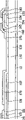
Fig. 1 is the layout according to the tft array plate of the LCD of the embodiment of the invention;
Fig. 2 is the layout according to the common electrical pole plate of the LCD of the embodiment of the invention;
Fig. 3 is the layout that comprises the LCD of the common electrical pole plate shown in the tft array plate shown in Fig. 1 and Fig. 2;
Fig. 4 is the sectional view that the IV-IV ' along the line of LCD shown in Fig. 3 is got;
Fig. 5 is the equivalent circuit diagram of LCD shown in Fig. 1 to 4;
Fig. 6 is the layout of LCD according to another embodiment of the present invention;
Fig. 7 is the sectional view that the VII-VII ' along the line of LCD shown in Fig. 6 is got;
Fig. 8 is the layout of LCD according to another embodiment of the present invention;
Fig. 9 is the layout of the tft array plate of LCD according to another embodiment of the present invention;
Figure 10 is the layout of the common electrical pole plate of LCD according to another embodiment of the present invention;
Figure 11 is the layout that comprises the LCD of the common electrical pole plate shown in the tft array plate shown in Fig. 9 and Figure 10;
Figure 12 is the layout of the tft array plate of LCD according to another embodiment of the present invention;
Figure 13 is the layout of the common electrical pole plate of LCD according to another embodiment of the present invention;
Figure 14 is the layout that comprises the LCD of the common electrical pole plate shown in the tft array plate shown in Figure 12 and Figure 13;
Figure 15 is the sectional view that the XV-XV ' along the line of LCD shown in Figure 14 is got;
Figure 16 A, Figure 17 A, Figure 18 A and Figure 20 A are the layouts according to tft array plate in the intermediate steps of the manufacture method of the plate of tft array shown in Figure 12 to 15 of the embodiment of the invention.
Figure 16 B, Figure 17 B, Figure 18 B and Figure 20 B are Figure 16 A, Figure 17 A, and tft array plate shown in Figure 18 A and Figure 20 A is XVIB-XVIB ' along the line respectively, XVIIB-XVIIB ', the sectional view that XVIIIB-XVIIIB ' and XXB-XXB ' got.
Figure 19 is the sectional view that tft array plate XVIIIB-XVIIIB ' along the line is got shown in Figure 18 A in the intermediate steps after step shown in Figure 18 B;
Figure 21 is the sectional view that tft array plate XXB-XXB ' along the line is got shown in Figure 20 A in the step after intermediate steps shown in Figure 20 B;
Figure 22 is the layout of LCD according to another embodiment of the present invention;
Figure 23 is the sectional view that the XXIII-XXIII ' along the line of LCD shown in Figure 22 is got;
Figure 24 is the layout of the tft array plate of LCD according to another embodiment of the present invention;
Figure 25 is the layout that comprises the LCD of the common electrical pole plate shown in the tft array plate shown in Figure 24 and Fig. 2;
Figure 26 is the sectional view that the XXVI-XXVI ' along the line of LCD shown in Figure 25 is got;
Figure 27 is the layout of the tft array plate of LCD according to another embodiment of the present invention;
Figure 28 is the layout that comprises the LCD of the common electrical pole plate shown in the tft array plate shown in Figure 27 and Fig. 2;
Figure 29 is the sectional view that the XXIX-XXIX ' along the line of LCD shown in Figure 28 is got.
Embodiment
After this will describe the present invention more all sidedly with reference to the accompanying drawings, accompanying drawing shows embodiments of the invention.Yet the present invention may be embodied as a lot of different forms and should not be construed as the embodiment that is confined in this proposition.
In the accompanying drawings, for clear layer, film and the regional thickness exaggerated.From start to finish, same Reference numeral is represented same element.The position of element can be described with reference to their directions in the drawings, for example upwards is exactly the top towards figure.Be understandable that, when element such as layer, film, zone or substrate be expressed as another element it " on " time, can directly can there be intermediary element in it on other elements or also.On the contrary, when element is expressed as " directly " on another element the time, just there has not been intermediary element.
With reference to figure 1, comprise tft array plate 100 according to the LCD of the embodiment of the invention, common electrical pole plate 200, and insert LC layer 3 between the plate 100 and 200.
Describe tft array plate 100 in detail with reference to figure 1, Fig. 3 and Fig. 4.
Comprise a plurality of grid conductors of many gate lines 121, many storage electrode lines 131 and a plurality of capacitance electrode 136, be formed on the insulated substrate 110 such as clear glass or plastics.
Each comprises wide lateral part and connected narrow longitudinal component with the capacitance electrode 136 that storage electrode line 131 separates, and wide lateral part comprises the outshot 139 that projects upwards.The lateral part is to be basically parallel to adjacent two gate lines 121 and from this basic equidistant rectangle that prolongs.Longitudinal component extends to storage electrode line 131 from the lateral part right-hand member.
Grid conductor 121,131 and 136 is preferably by metal such as Al or Al alloy, Ag or Ag alloy, and Cu or Cu alloy, Mo or Mo alloy, Cr, Ta, or Ti constitutes.Conductor also can have the sandwich construction that comprises the two-layer conducting film (not shown) with different physical characteristicss.One deck in the two membranes preferably includes low resistivity metal such as Al, Ag or Cu, to reduce signal delay or voltage drop.Another tunic preferably include have good physics, chemical characteristic and the metal such as the Mo of contact characteristics, Cr, Ta, or Ti are arranged with other material such as tin indium oxide (ITO) or indium zinc oxide (IZO).The example of two membranes combination has the Cr of lower floor film and upper strata Al (alloy) film, or the Al of lower floor (alloy) film and upper strata Mo (alloy) film.Yet as is known to the person skilled in the art, grid conductor 121,131 and 136 can be made by various metals or conductor.
Grid conductor 121,131 and 136 transverse side are with respect to the surface tilt of substrate 110, and such pitch angle can be at about 30 degree to the scopes of 80 degree.
Preferably the gate insulator 140 that is made of silicon nitride (SiNx) or monox (SiOx) forms on grid conductor 121,131 and 136.
Preferably many semiconductor stripeds of being made by amorphous silicon hydride (being abbreviated as " a-Si ") or polysilicon 151 form on gate insulator 140.Every semiconductor striped 151 extends substantially in a longitudinal direction and is widening near gate line 121 and storage electrode line 131 places, thus the large tracts of land of semiconductor striped 151 covering gate polar curves 121 and storage electrode line 131.Every semiconductor striped 151 has a plurality of outshots 154 towards grid 124 outside branches.
Many Ohmic contact stripeds and island 161 and 165 form on semiconductor striped 151.Ohmic contact striped and island 161 and 165 can be made of the n+ hydrogenation a-Si of for example heavy doping n type adulterant such as phosphorus or silicide.Every Ohmic contact striped 161 has a plurality of outshots 163, and outshot 163 and Ohmic contact island 165 are positioned on the outshot 154 of semiconductor striped 151 in couples.
The transverse side of semiconductor striped 151 and Ohmic contact 161 and 165 surface tilt with respect to substrate 110, these pitch angle can be at about 30 degree to the scope of 80 degree.
The a plurality of data conductors that comprise many data lines 171 and a plurality of drain electrode 175 Ohmic contact 161 and 165 and gate insulator 140 on form.
Each drain electrode 175 separates and comprises the narrow end that is oppositely arranged about grid 124 with source electrode 173 with data line 171.The end of drain electrode 175 is centered on by source electrode 173 parts.
Each drain electrode 175 also comprises extension 177 and is connected in this coupling electrode 176.
Only be inserted in Ohmic contact 161 and 165 between following semiconductor striped 151 and the top data conductor 171 and 175 and reduce contact resistance between the adjacent levels.Although semiconductor striped 151 is most of local narrower than data line 171, as mentioned above, semiconductor striped 151 is used for the profile of smooth surface widening near above-mentioned gate line 121 places, thereby prevents that data line 171 from disconnecting.Semiconductor striped 151 comprises does not have some of cover data conductor 171 and 175 expose portions, for example in source electrode 173 and the part between 175 of draining.
A plurality of colored filter (not shown) can be arranged between passivating film 180p of lower floor and the upper strata passivating film 180q, or replaceable upper strata passivating film 180q.
A plurality of pixel electrodes 190 and a plurality of auxiliary contact portion 81 and 82 form on passivation layer 180, and auxiliary contact portion is preferably made by transparent conductor such as ITO or IZO or reflection conductor such as Ag, Al, Cr or their alloy.
Each pixel electrode 190 can be the rectangle with the left comer of cutting sth. askew that favours gate line 121.Pixel electrode 190 overlaps with gate line 121, thereby increases the aperture ratio.
Each pixel electrode 190 has slit 92, and this slit is divided into outside and inner pixel electrode 190a and 190b with pixel electrode 190.
The bottom that slit 92 can comprise inclination and top 92a and 92b and the longitudinal component that is connected them.Bottom and top 92a and 92b extend to the left side from the right of pixel electrode 190.Longitudinal component 92c connects the left part of bottom and top 92a and 92b.
Therefore, inner pixel electrode 190b can be configured as the isosceles trapezoid at rotation one right angle, and outer sub-pixels electrode 190a comprise a pair of rotation one right angle right-angled trapezium and with the longitudinal component of right-angled trapezium coupling, it can be considered to upper and lower outer sub-pixels electrode part.
Outer sub-pixels electrode 190a can be electrically connected on extension 177 by contact hole 185.
The quantity of otch and the quantity of dividing plate are according to such as the size of pixel electrode 190, pixel electrode 190 horizontal edges and the ratio of longitudinal edge and the design factor of the characteristic of LC layer 3 and different for example.
With reference now to Fig. 2 to 4, common electrical pole plate 200 is described.
Be called black matrix" and be used to prevent that the photoresistance that light leaks from can form every parts 220 on such as the insulated substrate 210 of clear glass or plastics.Photoresistance has a plurality of openings 225 in the face of pixel electrode 190 every parts 220, and it can have and pixel electrode 190 essentially identical flat shapes.Different is, photoresistance can comprise a plurality of widened sections of a plurality of straight line portioies of the data line 171 on the tft array plate 100 and the TFT on the tft array plate 100 every parts 220.
A plurality of colored filters 230 also can form on substrate 210, and they are substantially disposed in by photoresistance in parts 220 region surrounded.Colored filter 230 can be substantially extends along the longitudinal direction of pixel electrode 190.Colored filter 230 can show such as a kind of color in red, the green or blue three primary colors.
One group of cut sides is to pixel electrode 190 and comprise center cut 71, lower cut-out 72a and upper cut-out 72b.Each otch 71-72b is arranged between the adjacent otch 91-92b, perhaps between the bevelled edge of otch 92a or 92b and pixel electrode 190.Each otch 71-72b has sloping portion at least, and this sloping portion has recessed recess and is parallel to lower cut-out 92a or upper cut-out 92b extension.Otch 71-72b can be symmetrical substantially with respect to capacitance electrode 136.
As shown in Figure 3, each bottom and upper cut-out 72a and 72b comprise approximately from pixel electrode 190 left sides sloping portion that extends to bottom or top edge, and the edge from each end of sloping portion along pixel electrode 190 extends, overlap with the edge of pixel electrode 190 and with the obtuse-angulate horizontal and vertical part of sloping portion.
Center cut 71 comprises about central cross part of extending from pixel electrode 190 left sides along horizontal line, a pair of sloping portion and a pair of terminal longitudinal component that extends along the right of pixel electrode 190 from the end of each sloping portion that approximately extends to the right of pixel electrode 190 from the end of lateral part, center, thereby is divided into the obtuse angle with the right hand edge overlapping of pixel electrode 190 and with each rake.
91-92b is the same with otch, and the quantity of otch 71-72b can be according to design factor and difference.And photoresistance also can overlap with otch 71-72b every parts 220 and leak with the light that intercepts by it.
Can be (homeotropic) in the same way oriented layer 11 and 21 and polaroid 12 and 22 can on the inside and outside surface of plate 100 and 200, provide respectively, make their polarization axle intersect and polarization axle in one can be parallel to gate line 121.When LCD is reflective LCD, can omit in polaroid 12 or 22.
LCD can comprise that also at least one is used to compensate the phase shift films (not shown) of the delay of LC layer 3.Phase shift films has birefringence and the opposite delay that is provided with LC layer 3 is provided.
LCD also can comprise by polaroid 12 and 22, phase shift films and plate 100 and 200 provides the back light unit (not shown) of light to LC layer 3.
Preferably, LC layer 3 has negative dielectric anisotropy, and its obeys homeotropic alignment, thereby LC molecule 310 is not when having electric field, basic and plate 100 and 200 surperficial quadratures with their longitudinal axis and arrange.Therefore, incident light can not pass through the polarized systems of the intersection of polarizer 12 and 22.
Replacedly, the pixel of LCD can comprise the TFT Q of first sub-pixel and second sub-pixel, and this first sub-pixel comprises a LC capacitor Clca and holding capacitor Cst, and this second sub-pixel comprises the 2nd LC capacitor Clcb and coupling condenser Ccp.
The one LC capacitor Clca comprises outer sub-pixels electrode 190a as a terminal, is arranged on therebetween part as medium as the appropriate section of the public electrode 270 of another terminal and LC layer 3.Similar, the 2nd LC capacitor Clcb have similar structure and comprise inside pixel electrode 190b as a terminal, as the appropriate section of the public electrode 270 of another terminal and LC layer 3 part as medium disposed thereon.
Memory capacitance Cst comprises the extension 177 as the drain electrode 175 of a terminal, and as the storage electrode 137 of another terminal, and gate insulator 140 places the part as medium therebetween.
Coupling capacitance Ccp comprises inside pixel electrode 190b and the capacitance electrode 136 as a terminal, and as the coupling electrode 176 of another terminal, and passivation layer 180 and gate insulator 140 place the part as medium therebetween.
The one LC capacitor C lca and memory capacitance Cst are connected in the drain electrode of TFT Q abreast.Coupling capacitance CCp is connected between the drain electrode and the 2nd LC capacitor C lcb of TFT Q.Public electrode 270 is supplied to common electric voltage Vcom, and this voltage is provided to storage electrode line 131.
TFT Q response provides data voltage from data line 171 to a LC capacitor Clca and coupling condenser Ccp from the signal of gate line 121, and coupling condenser Ccp transmits the data voltage with change size to the 2nd LC capacitor Clcb.
If storage electrode line 131 is supplied to common electric voltage Vcom, and each capacitor Clca, Cst, Clcb and Ccp and electric capacity thereof represents with identical fixed reference feature, is charged to following the providing of voltage Vb of the 2nd LC capacitor Clcb:
Vb=Va×[Ccp/(Ccp+Clcb)],
Here Va represents the voltage of a LC capacitor Clca.
Because Ccp/ (Ccp+Clcb) is less than the voltage Vb of 1, the two LC capacitor Clcb voltage less than a LC capacitor Clca.The situation that this unequal voltage at storage electrode line 131 is not equal to common electric voltage Vcom also is correct.
When in a LC capacitor Clca or the 2nd LC capacitor Clcb generation electric potential difference, in LC layer 3, produce the electric field of the surperficial quadrature of basic and plate 100 and 200, pixel electrode 190 and public electrode 270 generally all are called a generating electrodes hereinafter.Then, the LC molecule 310 in the LC layer 3 responds electric fields and tilts, thus their longitudinal axis and field direction quadrature.The degree of tilt of LC molecule 310 determines that polarization of incident light changes on the LC layer 3, and this polarization variations changes the variation of the light that is passed through by polaroid 12 and 22 into.Like this, LCD display image.
The intensity of electric field is depended at the pitch angle of LC molecule 310.Because the voltage Vb of a LC capacitor Clca and the voltage Va of the 2nd LC capacitor Clcb are differing from each other, the vergence direction of LC molecule 310 is different from the vergence direction of LC molecule 310 in second sub-pixel in first sub-pixel, and the brightness of such two sub-pixels is just different.Therefore, remain on object brightness by the mean flow rate that makes two sub-pixels, can adjust the voltage Va and the Vb of first and second sub-pixels, the image of observing from transverse side approaches from the image of observing previously most like this, thereby has improved side visibility.
The ratio of voltage Va and Vb can be adjusted by the electric capacity that changes coupling capacitance Ccp, and coupling capacitance Ccp can change by overlapping area and the distance that changes between coupling electrode 176 and the inner pixel electrode 190b (and capacitance electrode 136).For example, when capacitance electrode 136 moves and coupling electrode 176 when moving on the position before the capacitance electrode 136, the distance between coupling electrode 176 and the inner pixel electrode 190b becomes big.Preferably, the voltage Vb of the 2nd LC capacitor C lcb approximately is 0.6 to 0.8 times of voltage Va of a LC capacitor C lca.
The voltage Vb that is filled in the 2nd LC capacitor Clcb can be greater than the voltage Va of a LC capacitor Clca.This is by realizing such as the predetermined voltage of common electric voltage Vcom the 2nd LC capacitor Clcb preliminary filling.
The inside pixel electrode 190b of second sub-pixel preferably approximately be first sub-pixel outer sub-pixels electrode 190a width 0.8-1.5 doubly, the quantity of the pixel electrode in each LC capacitor Clca and Clcb can change.
The vergence direction of LC molecule 310 is subjected to horizontal component that is produced by the otch 91-92b of field generating electrodes 190 and 270 and 71-72b and the lopsided influence that makes the pixel electrode 190 of electrical field deformation, the vergence direction of LC molecule basic and the edge of otch 91-92b and 71-72b and the inclined side quadrature of pixel electrode 190.With reference to 3, one groups of otch 91-92b of figure and 71-72b pixel electrode 190 is divided into a plurality of subregions, and each subregion have two long limits.Because the LC molecule 310 on each subregion tilts perpendicular to long limit, the orientation of vergence direction distributes and is positioned at four direction, thereby has increased the reference viewing angle of LCD.
Recess in the otch 71-72b determines that otch 71-72b goes up the vergence direction of LC molecule 310, and they can provide and also can have different shapes and arrangement at otch 91-92b.
Determine that the otch 91-92b of LC molecule 310 vergence directions and shape and the arrangement of 71-72b can change, and at least one otch can be highlighted body (not shown) or the replacement of sagging body (not shown) among 91-92b and the 71-72b.The top or the bottom of generating electrodes 190 on the scene or 270 can be made and be provided with to excrescence by the organic or inorganic material.
Describe LCD according to another embodiment of the present invention in detail with reference to figure 6 and 7.
Identical with shown in Fig. 1 to 4 basically according to the plate 100 of this embodiment and 200 layer structure.
Yet in this embodiment, semiconductor striped 151 and data line 171 and drain electrode 175 and bottom Ohmic contact 161 and 165 almost have identical flat shape.But semiconductor striped 151 comprises the expose portion that some are not covered by data line 171 and drain electrode 175, and for example semiconductor striped 151 is in source electrode 173 and the part between 175 of draining.
In addition, capacitance electrode 136 does not have sloping portion, and each drain electrode 175 comprises that being parallel to data line 171 extends and connect extension 177 and near the interconnect portion 178 of the coupling electrode 176 of its left surface.
For example, the manufacture method of the tft array plate shown in Fig. 4 and Fig. 7 is used a lithography step, forms data line 171, drain electrode 175, semiconductor 151 and Ohmic contact 161 and 165 simultaneously.
The photoresist mask pattern that is used for photoetching process has different-thickness, and particularly, it has than thickness portion and thin part.Be positioned on the wiring zone that data line 171 and drain electrode 175 will occupy than thickness portion, thin part is positioned on the TFT channel region.
The thickness that changes with the position of photoresist obtains by several technology, for example, and by on the exposure mask, providing translucent area and transparent region and photoresistance every zone of opacity.Translucent area can have slit pattern, grid pattern, perhaps one deck or more multi-layered film with middle visibility or interior thickness.When using slit pattern, the width of preferred slit or the distance between slit are less than the resolution of the exposer that is used for photoetching (light exposer).Another example is to use again, and the time causes resist.At length, in case form by using the rotine exposure mask that only has transparent region and zone of opacity by flowing the photoresist mask that material constitutes again, will pass through reflow process, wherein material can flow to the zone that does not have photoresist, thereby forms thin part.
As a result, manufacture process obtains simplifying by omitting lithography step.
Describe LCD according to another embodiment of the present invention in detail with reference to figure 8, it has and the essentially identical layer of LCD shown in Fig. 1 to 4 structure.
Yet in the LCD of Fig. 8, each coupling electrode 176 extends upward and turns to from the extension 177 of drain electrode 175 along the center cut 71 of public electrode 270 and extends.Capacitance electrode 136 has and coupling electrode 176 essentially identical shapes, except the outshot 139 that contacts with pixel electrode 190b.
The light that coupling electrode 176 and capacitance electrode 136 intercepts near otch 71 places leaks, and is reduced by the invalid part of electrode 176 and 136 occupied regional transmissions, thereby increases the aperture ratio.
Describe LCD according to another embodiment of the present invention in detail with reference to figure 9, Figure 10 and Figure 11.
In this embodiment, each pixel electrode has 5 otch 93,94,95,96a and 96b.Otch 95 is pixel electrode 190 to be divided into the gap of pixel electrode 190a and 190b and the otch 93 in the pixel electrode 190b extend along the lateral part of capacitance electrode 136 and have a inlet on the right of pixel electrode 190.Otch 94 in the pixel electrode 190b comprises the lateral part of the weak point that extends along the lateral part of capacitance electrode 136, and a pair of sloping portion that tilts to extend towards the right of pixel electrode 190.Each otch 96a in the pixel electrode 190a and 96b approximately extend to the center, about left side of pixel electrode 190 from the bottom or the top of pixel electrode 190.
Similar, public electrode 270 comprises one group of 6 otch 73,74,75a, 75b, 76a and 76b.Each otch 73 and 74 comprises the central cross part, pair of angled part and a pair of terminal longitudinal component.Each otch 75a-76b comprises sloping portion and a pair of horizontal and vertical part or a pair of longitudinal component.In addition, otch 75a and 75b comprise the extension.The sloping portion that the sloping portion of otch 73-76b is parallel to otch 93-96b extends.
Describe LCD according to another embodiment of the present invention in detail with reference to Figure 12, Figure 13, Figure 14 and Figure 15.
According to the layer structure of the plate 100 of this embodiment and 200 substantially the same with shown in the previous embodiment.
Yet, in the LCD of this embodiment, do not have capacitance electrode.
Equidistant and the storage electrode 137 of every storage electrode line 131 and two adjacent gate lines 121 is externally gone up with inner pixel electrode 190a and 190b and is extended.Coupling electrode 176 is can be completely overlapping and disconnect with drain electrode 175 physics with storage electrode 137, the extension that coupling electrode does not overlap with storage electrode line 131.
Upper strata passivating film 180q has a plurality of openings 188 that are arranged on the coupling electrode 176, and lower membrane 180p has a plurality of contact holes 187 that are arranged on exposure coupling electrode 176 in the opening 188.
Each outer sub-pixels electrode 190a comprises lower part and the top that is linked to each other by longitudinal component, and the outer sub-pixels electrode has the outshot 191 that is connected in coupling electrode 176 by contact hole 187.
Now, describe for example manufacture method of the tft array plate shown in Figure 15 in detail with reference to figures 16A to Figure 21.
With reference to figure 16A and Figure 16 B, the conducting stratum that preferably is made of metal for example is deposited on the insulated substrate 110 by sputtering method.Then, conducting stratum comprises many gate lines 121 of grid 124 and end 129 and many storage electrode lines 131 that comprise storage electrode 137 through photoetching and etching formation.
Present 17A with the aid of pictures and Figure 17 B, gate insulator 140, intrinsic amorphous silicon layer and extrinsic amorphous silicon layer sequential aggradation.Extrinsic and intrinsic amorphous silicon layer comprises many extrinsic semiconductor stripeds 164 and many intrinsic semiconductor stripeds 151 of outshot 154 by photoetching and etching composition with formation.
As shown in Figure 18 A and Figure 18 B, conducting stratum for example deposits by sputtering method, and by photoetching and etching composition, comprises many data lines 171, a plurality of drain electrode 175 and a plurality of coupling electrode 176 of source electrode 173 and end 179 with formation.
Thereafter, the not cover data line 171 of extrinsic semiconductor striped or the expose portion of drain electrode 175 are removed, thereby finish a plurality of Ohmic contact island 161 and 165 and the part of intrinsic semiconductor striped 151 is exposed.Preferably carry out oxygen plasma treatment subsequently, in order to the exposed surface of stabilization of semiconductor striped 151.
With reference to Figure 19, deposition lower membrane 180p and upper layer film 180q comprise that the thickness portion 52 that is arranged on the regional A and the photoresist mask parts of the thin part 54 on the area B form on upper layer film 180q.Zone C does not have photoresist.Mask parts 52 and 54 can obtain by aforementioned techniques with reference to figure 6 and Fig. 7 with the thickness of change in location.
The expose portion of the upper and lower film 180q and 180p and zone C inner grid insulation course 140 are removed, to form a plurality of contact holes 181,182,185 and 186.By this step, only can make contact hole 181,182,185 and 186 top.
Below, with reference to figure 20A and Figure 20 B, mask parts 52 and 54, are removed so that the surface of upper layer film 180q exposes up to thin part 54 for example by polishing (ashing) through reduced down in thickness.
See Figure 21, the expose portion of upper layer film 180q is removed to form a plurality of openings 188.When not finishing contact hole 181,182,185 and 186 o'clock, layer 180q, 180p and 140 not removal part are removed in this step.
At last, has about 500-1,500
The ITO or the IZO layer of thickness for example deposit by sputtering method, and by photoetching and etching composition, to form a plurality of pixel electrodes 190 and a plurality of auxiliary contact portion 81 and 82 as shown in Figure 12 to Figure 15.
Describe LCD according to another embodiment of the present invention in detail with reference to Figure 22 and Figure 23, the plate 100 and 200 that it had has the layer structure similar to the previous embodiment shown in Figure 12 to 15.
Here, semiconductor striped 151 has identical flat shape with data line 171 and drain electrode 175 and bottom Ohmic contact 161 and 165.Yet semiconductor striped 151 comprises some expose portions that do not have cover data line 171 and drain electrode 175, just as in source electrode 173 and those parts between 175 of draining.
In addition, a plurality of semiconductor islands 156 and a plurality of Ohmic contact island 166 form below coupling electrode 176.
Can make the tft array plate according to short-cut method, this short-cut method uses simultaneously formation data line 171 of a lithography step, drain electrode 175, coupling electrode 176, semiconductor 151 and 156 and Ohmic contact 161,165 and 166.
Describe LCD according to another embodiment of the present invention in detail with reference to Figure 24, Figure 25 and Figure 26, wherein plate 100 and 200 layer structure are substantially the same with previous embodiment.
In the present embodiment, each outer sub-pixels electrode 190a is divided into lower part and top 190a1 and 190a2 (after this being called bottom and top pixel electrode), and they are positioned opposite to each other about inner pixel electrode 190b.That is to say that each otch 92 comprises two the sloping portion 92a and the 92b of straight line discrete pixels electrode 190.Therefore, otch 92 does not have longitudinal component, and does not connect the longitudinal component of the part of outer sub-pixels electrode 190a.
Therefore, inner pixel electrode 190b extends to the left side of pixel electrode 190 to increase the aperture ratio.
Each capacitance electrode 136 is provided with and is basically parallel to data line 171 prolongations near the left side of pixel electrode 190, to cover the part of bottom and top pixel electrode 190a1 and 190a2.Capacitance electrode 136 comprises outshot 139, and this outshot can be exposed also by contact hole 186 can be connected in inner pixel electrode 190b.Contact hole 186 is arranged on from otch 91 and extends, do not belong on the straight line of effective viewing area, thereby improves display characteristic.
Each coupling electrode 176 is overlapping and similar with its shape with capacitance electrode 136, except that outshot 139.Each drain electrode 175 also comprises the interconnect portion 178 that connects extension 177 and coupling electrode 176.Interconnect portion 178 tilts to extend along otch 72a, to intercept the light leakage of passing through it and to increase the aperture ratio.
The aperture of LCD shown in Figure 24 to Figure 26 is than through calculating aperture than LCD shown in Fig. 1 to Fig. 4 than big 4%-5%.
With reference to Figure 27, Figure 28 and Figure 29 describe LCD according to another embodiment of the present invention in detail, and be wherein pixel arrangement similar to pixel described in Figure 24 to Figure 26.
Yet in this embodiment, each drain electrode 175 also comprises coupling electrode 176 is connected to drain electrode 175 bottom interconnect portion 178a1 and the top interconnect portion 178a2 that extends to top pixel electrode 190a2 from coupling electrode 176.Bottom interconnect portion 178a1 extends along otch 72a inclination, thereby the light that intercepts by it leaks, and thereby increase aperture ratio.Then, commentaries on classics is connected in coupling electrode 176 thereby bottom interconnect portion 178a1 makes progress.
In addition, the contact hole 185a1 that exposes bottom interconnect portion 178a1 another contact hole 185a2 that can provide and expose top interconnect portion 178a2 at the steering position of interconnect portion 178a1 provides in the upper end of top interconnect portion.Bottom and top pixel electrode 190a1 and 190a2 are connected in bottom and top interconnect portion 178a1 and 178a2 by contact hole 185a1 and 185a2 respectively.
The aperture of present embodiment LCD is than through calculating aperture than LCD shown in Figure 12 to Figure 15 than big 2%-4%.
The present invention can be applied to distortion (twisted) to row (TN) mode LCD or XY switch (in-plane switching) mode LCD.
Though describe the present invention in detail with reference to some embodiment here, those skilled in the art can know, under the prerequisite that does not break away from the spirit and scope of the present invention of illustrating as appended claim, can carry out various modification and replacement to it.
The application requires the right of priority of on July 27th, 2004 at the No.10-2004-0058709 korean patent application of Korea S Department of Intellectual Property application, and its full content is incorporated herein by reference.
Claims (25)
1, a kind of film transistor array plate comprises:
Substrate;
First signal wire is formed on this substrate;
The secondary signal line intersects with this first signal wire;
Thin film transistor (TFT) is connected in this first signal wire and this secondary signal line;
Pixel electrode, it comprises first sub-pixel part and the second sub-pixel part and the 3rd sub-pixel part that is electrically connected on this thin film transistor (TFT), and
Coupling electrode is electrically connected on this first sub-pixel part and this second sub-pixel part, wherein this coupling electrode and the 3rd sub-pixel partition capacitance coupling.
2, according to the film transistor array plate of claim 1, wherein this first sub-pixel part and this second sub-pixel part are positioned opposite to each other about the 3rd sub-pixel part.
3,, also be included in the storage electrode of the bottom of at least one in this first sub-pixel part, this second sub-pixel part and this coupling electrode according to the film transistor array plate of claim 1.
4, according to the film transistor array plate of claim 1, wherein this coupling electrode is in the bottom of the 3rd sub-pixel part.
5, according to the film transistor array plate of claim 4, also comprise the insulation course that is arranged between this coupling electrode and this pixel electrode, wherein the part of this insulation course is arranged between this coupling electrode and the 3rd sub-pixel part also thin than other parts of this insulation course.
6, according to the film transistor array plate of claim 5, wherein this insulation course comprises inoranic membrane and organic membrane.
7, according to the film transistor array plate of claim 6, wherein this organic membrane has the opening that is arranged on this coupling electrode, and wherein this coupling electrode is coupled to the 3rd sub-pixel part to form coupling condenser by this opening in this organic membrane.
8,, also comprise being electrically connected on the 3rd sub-pixel part and at the capacitance electrode of this coupling electrode bottom according to the film transistor array plate of claim 4.
9, film transistor array plate according to Claim 8 also comprises:
First insulation course is arranged between this first signal wire and this secondary signal line, and wherein this first insulation course also is arranged between this capacitance electrode and this coupling electrode; And
Second insulation course is arranged between this secondary signal line and this pixel electrode, and wherein this second insulation course also is arranged between this coupling electrode and the 3rd sub-pixel part.
10, according to the film transistor array plate of claim 9, wherein this second insulation course comprises inoranic membrane and the organic membrane that is arranged on this inoranic membrane.
11, film transistor array plate according to Claim 8 also comprises:
Be arranged on the insulation course between this first signal wire and this secondary signal line, wherein this insulation course also is arranged between this capacitance electrode and this coupling electrode.
12, according to the film transistor array plate of claim 1, wherein this coupling electrode extends from this thin film transistor (TFT).
13,, also comprise the capacitance electrode that is electrically connected on the 3rd sub-pixel part and is coupled with this first sub-pixel part or this second sub-pixel partition capacitance according to the film transistor array plate of claim 1.
14,, also comprise the insulation course that is arranged between this secondary signal line and this pixel electrode according to the film transistor array plate of claim 1.
15, according to the film transistor array plate of claim 14, wherein this insulation course comprises inoranic membrane and the organic membrane that is arranged on this inoranic membrane.
16,, also comprise this pixel electrode is divided into this first sub-pixel part the partition member of this second sub-pixel part and the 3rd sub-pixel part according to the film transistor array plate of claim 1.
17, according to the film transistor array plate of claim 1, wherein this first sub-pixel part and this second sub-pixel part are spaced apart.
18, a kind of LCD panel comprises:
The common electrical pole plate comprises public electrode;
Film transistor array plate, this public electrode is provided with relatively, and this film transistor array plate comprises:
Substrate,
First signal wire is formed on this substrate,
The secondary signal line intersects with this first signal wire,
Thin film transistor (TFT) is connected in this first signal wire and this secondary signal line,
Pixel electrode, it comprises first sub-pixel part and the second sub-pixel part and the 3rd sub-pixel part that is electrically connected on this thin film transistor (TFT), and
Coupling electrode is electrically connected on this first sub-pixel part and this second sub-pixel part, wherein this coupling electrode and the 3rd sub-pixel partition capacitance coupling; And
Liquid crystal layer is arranged between this common electrical pole plate and this film transistor array plate.
19, according to the LCD panel of claim 18, wherein:
This pixel electrode comprises:
First sub-pixel comprises this first sub-pixel part or this second sub-pixel part of being applied with first voltage,
And second sub-pixel, comprise the 3rd sub-pixel part.
20, according to the LCD panel of claim 19, wherein:
This first sub-pixel comprises first liquid crystal capacitor and holding capacitor; And
This second sub-pixel comprises second liquid crystal capacitor and coupling condenser.
21, according to the LCD panel of claim 20, wherein:
This first liquid crystal capacitor comprises: have this first sub-pixel part and second sub-pixel part first terminal, comprise first of this public electrode overlap part second terminal and be arranged on first terminal of this first liquid crystal capacitor and second terminal between as a part of liquid crystal layer of medium; And
This second liquid crystal capacitor comprises: have the 3rd sub-pixel part first terminal, comprise second of this public electrode overlap part second terminal and be arranged on first terminal of this second liquid crystal capacitor and second terminal between as a part of liquid crystal layer of medium.
22, according to the LCD panel of claim 19, wherein second voltage is applied to the 3rd sub-pixel part, and this first voltage is greater than this second voltage.
23, according to the LCD panel of claim 22, wherein this second voltage is 60% to 80% of this first voltage.
24, according to the LCD panel of claim 21, wherein:
This holding capacitor comprise the extension of drain electrode with this thin film transistor (TFT) first terminal, comprise second terminal of the storage electrode that is arranged on this substrate and be arranged on first terminal of this holding capacitor and second terminal between as a part of gate insulator of medium; And
Second terminal of the coupling electrode that this coupling condenser comprises first terminal that has the 3rd sub-pixel part and be arranged on the capacitance electrode on this substrate, comprise the extension that is electrically connected on this drain electrode and be arranged on first terminal of this coupling condenser and second terminal between as the part of grid pole insulation course and the passivation layer of medium.
25, according to the LCD panel of claim 24, wherein by changing the position of this coupling electrode with respect to this first sub-pixel part and second sub-pixel part, the electric capacity of this coupling condenser is changed, thereby adjust the ratio of this first voltage and this second voltage.
Applications Claiming Priority (2)
| Application Number | Priority Date | Filing Date | Title |
|---|---|---|---|
| KR58709/04 | 2004-07-27 | ||
| KR1020040058709A KR101112539B1 (en) | 2004-07-27 | 2004-07-27 | Liquid crystal display having multi domain and panel for the same |
Publications (2)
| Publication Number | Publication Date |
|---|---|
| CN1755470A CN1755470A (en) | 2006-04-05 |
| CN100559251C true CN100559251C (en) | 2009-11-11 |
Family
ID=36688826
Family Applications (1)
| Application Number | Title | Priority Date | Filing Date |
|---|---|---|---|
| CNB2005101067616A Active CN100559251C (en) | 2004-07-27 | 2005-07-27 | LCD panel and film transistor array plate |
Country Status (6)
| Country | Link |
|---|---|
| US (1) | US7483090B2 (en) |
| EP (1) | EP1621924B1 (en) |
| JP (1) | JP4791099B2 (en) |
| KR (1) | KR101112539B1 (en) |
| CN (1) | CN100559251C (en) |
| TW (1) | TWI424221B (en) |
Families Citing this family (28)
| Publication number | Priority date | Publication date | Assignee | Title |
|---|---|---|---|---|
| KR101189266B1 (en) * | 2004-09-24 | 2012-10-09 | 삼성디스플레이 주식회사 | Liquid crystal display |
| US8049699B2 (en) * | 2005-02-07 | 2011-11-01 | Samsung Electronics Co., Ltd. | Liquid crystal display apparatus having storage electrodes overlapping only some sub-pixels |
| US7936407B2 (en) * | 2005-02-24 | 2011-05-03 | Samsung Electronics Co., Ltd. | Array substrate, method of manufacturing the same, display panel having the same, and liquid crystal display apparatus having the same |
| JP5144055B2 (en) * | 2005-11-15 | 2013-02-13 | 三星電子株式会社 | Display substrate and display device having the same |
| KR101231867B1 (en) * | 2006-02-23 | 2013-02-08 | 삼성디스플레이 주식회사 | Liquid Crystal Display Apparatus |
| KR20070087395A (en) * | 2006-02-23 | 2007-08-28 | 삼성전자주식회사 | Display panel |
| US7710524B2 (en) * | 2006-03-15 | 2010-05-04 | Quanta Display, Inc. | Liquid crystal display with compensated pixel arrays |
| KR20070099287A (en) * | 2006-04-04 | 2007-10-09 | 삼성전자주식회사 | Liquid crystal composition and liquid crystal display comprising the same |
| KR20080010159A (en) * | 2006-07-26 | 2008-01-30 | 삼성전자주식회사 | Liquid crystal display |
| KR101267496B1 (en) * | 2006-08-09 | 2013-05-31 | 삼성디스플레이 주식회사 | Liquid crystal display |
| KR20080024285A (en) * | 2006-09-13 | 2008-03-18 | 삼성전자주식회사 | Liquid crystal composition and liquid crystal display comprising the same |
| US8159640B2 (en) * | 2006-09-22 | 2012-04-17 | Sharp Kabushiki Kaisha | Liquid crystal display device |
| KR20080028572A (en) * | 2006-09-27 | 2008-04-01 | 삼성전자주식회사 | Liquid crystal composition and liquid crystal display comprising the same |
| CN101165578B (en) * | 2006-10-18 | 2011-08-17 | 奇美电子股份有限公司 | Multidomain vertical orientation liquid crystal display panel |
| KR101437870B1 (en) * | 2008-02-15 | 2014-09-05 | 삼성디스플레이 주식회사 | Vertically aligned liquid crystal display and manufacturing method of the same |
| US8432344B2 (en) * | 2008-05-27 | 2013-04-30 | Samsung Display Co., Ltd. | Liquid crystal display |
| KR20090126764A (en) | 2008-06-05 | 2009-12-09 | 삼성전자주식회사 | Display substrate, method for manufacturing the display substrate and display device having the display substrate |
| JP5107439B2 (en) * | 2008-11-05 | 2012-12-26 | シャープ株式会社 | Active matrix substrate, liquid crystal panel, liquid crystal display unit, liquid crystal display device, television receiver |
| US8847352B2 (en) | 2008-11-05 | 2014-09-30 | Sharp Kabushiki Kaisha | Active matrix device including first and second capacitor electrodes and multiple capacitors |
| US20120001839A1 (en) * | 2009-03-05 | 2012-01-05 | Sharp Kabushiki Kaisha | Active matrix substrate, liquid crystal panel, liquid crystal display device, liquid crystal display unit, and television receiver |
| US8698969B2 (en) | 2009-03-05 | 2014-04-15 | Sharp Kabushiki Kaisha | Active matrix substrate, method for producing active matrix substrate, liquid crystal panel, method for producing liquid crystal panel, liquid crystal display device, liquid crystal display unit, and television receiver |
| US8976209B2 (en) | 2009-03-05 | 2015-03-10 | Sharp Kabushiki Kaisha | Active matrix substrate, method for producing active matrix substrate, liquid crystal panel, method for producing liquid crystal panel, liquid crystal display device, liquid crystal display unit, and television receiver |
| KR101592014B1 (en) | 2009-03-10 | 2016-02-19 | 삼성디스플레이 주식회사 | Liquid crystal display |
| KR101888032B1 (en) * | 2011-07-28 | 2018-08-14 | 엘지디스플레이 주식회사 | Array substrate for In-Plane switching mode liquid crystal display device |
| KR101908460B1 (en) * | 2011-09-29 | 2018-10-17 | 삼성디스플레이 주식회사 | Display substrate, method of manufacturing the same and display apparatus having the same |
| KR102141167B1 (en) | 2013-12-12 | 2020-08-05 | 삼성디스플레이 주식회사 | Liquid crystal display |
| KR102389875B1 (en) * | 2015-09-01 | 2022-04-22 | 삼성디스플레이 주식회사 | Liquid crystal display device |
| CN106773413A (en) * | 2017-01-03 | 2017-05-31 | 深圳市华星光电技术有限公司 | A kind of array base palte and display device |
Family Cites Families (23)
| Publication number | Priority date | Publication date | Assignee | Title |
|---|---|---|---|---|
| US5245450A (en) * | 1990-07-23 | 1993-09-14 | Hosiden Corporation | Liquid crystal display device with control capacitors for gray-scale |
| JP2590693B2 (en) * | 1993-07-14 | 1997-03-12 | 日本電気株式会社 | Liquid crystal display |
| JPH07325323A (en) * | 1994-06-02 | 1995-12-12 | Matsushita Electric Ind Co Ltd | Liquid crystal display device |
| KR0141774B1 (en) * | 1994-06-17 | 1998-06-15 | 구자홍 | Liquid crystal display device and its manufacturing method |
| KR970011972A (en) * | 1995-08-11 | 1997-03-29 | 쯔지 하루오 | Transmission type liquid crystal display device and manufacturing method thereof |
| DE19712233C2 (en) * | 1996-03-26 | 2003-12-11 | Lg Philips Lcd Co | Liquid crystal display and manufacturing method therefor |
| JP3658849B2 (en) * | 1996-03-29 | 2005-06-08 | セイコーエプソン株式会社 | Liquid crystal display element and manufacturing method thereof |
| CN1148600C (en) | 1996-11-26 | 2004-05-05 | 三星电子株式会社 | Liquid crystal display using organic insulating material and manufacturing methods thereof |
| KR19990003712A (en) * | 1997-06-26 | 1999-01-15 | 김영환 | Ultra high aperture liquid crystal display device and manufacturing method thereof |
| JPH1138439A (en) | 1997-07-16 | 1999-02-12 | Toshiba Corp | Active matrix substrate, its manufacture and active matrix liquid crystal display device |
| JPH11109390A (en) | 1997-09-30 | 1999-04-23 | Toshiba Corp | Liquid crystal display device |
| JP2000081636A (en) | 1998-09-03 | 2000-03-21 | Seiko Epson Corp | Electrooptical device and its manufacture and electronic instrument |
| KR100312753B1 (en) | 1998-10-13 | 2002-04-06 | 윤종용 | Wide viewing angle liquid crystal display device |
| JP3484363B2 (en) | 1998-11-24 | 2004-01-06 | 株式会社 日立ディスプレイズ | Liquid crystal display |
| KR100379287B1 (en) * | 1999-06-25 | 2003-04-10 | 닛뽄덴끼 가부시끼가이샤 | Multi domain LCD device |
| KR100366081B1 (en) | 2000-04-27 | 2002-12-26 | 삼성에스디아이 주식회사 | Active matrix type displayer for progressing aperture ratio and method for manufacturing as the same |
| KR100380141B1 (en) | 2000-09-25 | 2003-04-11 | 엘지.필립스 엘시디 주식회사 | array panel for liquid crystal display and fabricating method of the same |
| TW513604B (en) * | 2001-02-14 | 2002-12-11 | Au Optronics Corp | A thin film transistor liquid crystal display |
| KR100413512B1 (en) | 2001-03-28 | 2003-12-31 | 엘지.필립스 엘시디 주식회사 | an array panel for liquid crystal display and manufacturing method thereof |
| KR100417917B1 (en) | 2002-04-03 | 2004-02-11 | 엘지.필립스 엘시디 주식회사 | Transreflective type Liquid Crystal Display Device and Method of Fabricating the same |
| KR100917766B1 (en) * | 2002-12-31 | 2009-09-15 | 엘지디스플레이 주식회사 | Liquid crystal display device and fabrication method for liquid crystal display |
| KR100961941B1 (en) * | 2003-01-03 | 2010-06-08 | 삼성전자주식회사 | Thin film transistor array panel for multi-domain liquid crystal display |
| JP4459685B2 (en) * | 2004-03-31 | 2010-04-28 | 富士通株式会社 | Liquid crystal display |
-
2004
- 2004-07-27 KR KR1020040058709A patent/KR101112539B1/en active IP Right Grant
-
2005
- 2005-07-26 JP JP2005216211A patent/JP4791099B2/en active Active
- 2005-07-27 CN CNB2005101067616A patent/CN100559251C/en active Active
- 2005-07-27 EP EP05254679.3A patent/EP1621924B1/en active Active
- 2005-07-27 TW TW094125426A patent/TWI424221B/en active
- 2005-07-27 US US11/189,835 patent/US7483090B2/en active Active
Also Published As
| Publication number | Publication date |
|---|---|
| JP2006039567A (en) | 2006-02-09 |
| CN1755470A (en) | 2006-04-05 |
| EP1621924A2 (en) | 2006-02-01 |
| JP4791099B2 (en) | 2011-10-12 |
| EP1621924B1 (en) | 2015-07-08 |
| KR20060010118A (en) | 2006-02-02 |
| TWI424221B (en) | 2014-01-21 |
| US20060028590A1 (en) | 2006-02-09 |
| EP1621924A3 (en) | 2006-05-17 |
| TW200615619A (en) | 2006-05-16 |
| KR101112539B1 (en) | 2012-02-15 |
| US7483090B2 (en) | 2009-01-27 |
Similar Documents
| Publication | Publication Date | Title |
|---|---|---|
| CN100559251C (en) | LCD panel and film transistor array plate | |
| CN100507687C (en) | Liquid crystal display and panel therefor | |
| CN1769990B (en) | Thin film transistor array panel | |
| CN1808252B (en) | Thin film transistor array panel and liquid crystal display including the panel | |
| CN100487897C (en) | Thin film transistor array panel and manufacturing method thereof | |
| US7324170B2 (en) | Liquid crystal display having subpixels per color pixel | |
| CN100465745C (en) | Liquid crystal display with wide viewing angle | |
| CN1605921B (en) | Liquid crystal display and thin film transistor substrate therefor | |
| CN100432803C (en) | Liquid crystal display | |
| CN100451780C (en) | Liquid crystal display and panel therefor | |
| US7619694B2 (en) | Thin film transistor array panel and manufacturing method thereof | |
| US7777823B2 (en) | Thin film transistor array panel | |
| CN100414409C (en) | Multi-zone liquid crystal display | |
| CN100578323C (en) | Liquid crystal display with wide viewing angle | |
| CN1573488B (en) | Liquid crystal display and thin film transistor array panel therefor | |
| CN100517727C (en) | Thin film transistor array panel | |
| US7474363B2 (en) | Liquid crystal display and panel therefor | |
| US7847907B2 (en) | Display substrate, method of fabricating the same, and liquid crystal display device having the same | |
| KR20150046923A (en) | Thin film transistor substrate and liquid crystal display | |
| CN1873508B (en) | Display panel and liquid crystal display apparatus including the same | |
| KR20080024697A (en) | Liquid crystal display | |
| KR101071252B1 (en) | Multi-domain liquid crystal display | |
| KR20160047032A (en) | Liquid crystal display | |
| KR20040097763A (en) | Multi-domain liquid crystal display and thin film transistor panel thereof | |
| KR20070026910A (en) | Liquid crystal display |
Legal Events
| Date | Code | Title | Description |
|---|---|---|---|
| C06 | Publication | ||
| PB01 | Publication | ||
| C10 | Entry into substantive examination | ||
| SE01 | Entry into force of request for substantive examination | ||
| C14 | Grant of patent or utility model | ||
| GR01 | Patent grant | ||
| ASS | Succession or assignment of patent right |
Owner name: SAMSUNG DISPLAY CO., LTD. Free format text: FORMER OWNER: SAMSUNG ELECTRONICS CO., LTD. Effective date: 20121106 |
|
| C41 | Transfer of patent application or patent right or utility model | ||
| TR01 | Transfer of patent right |
Effective date of registration: 20121106 Address after: Gyeonggi Do, South Korea Patentee after: Samsung Display Co., Ltd. Address before: Gyeonggi Do, South Korea Patentee before: Samsung Electronics Co., Ltd. |