CN100524644C - Dummy structures to reduce metal recess in electropolishing process - Google Patents
Dummy structures to reduce metal recess in electropolishing process Download PDFInfo
- Publication number
- CN100524644C CN100524644C CNB028165098A CN02816509A CN100524644C CN 100524644 C CN100524644 C CN 100524644C CN B028165098 A CNB028165098 A CN B028165098A CN 02816509 A CN02816509 A CN 02816509A CN 100524644 C CN100524644 C CN 100524644C
- Authority
- CN
- China
- Prior art keywords
- virtual
- semiconductor structure
- metal level
- groove
- groove area
- Prior art date
- Legal status (The legal status is an assumption and is not a legal conclusion. Google has not performed a legal analysis and makes no representation as to the accuracy of the status listed.)
- Expired - Fee Related
Links
Images


Classifications
-
- H—ELECTRICITY
- H01—ELECTRIC ELEMENTS
- H01L—SEMICONDUCTOR DEVICES NOT COVERED BY CLASS H10
- H01L21/00—Processes or apparatus adapted for the manufacture or treatment of semiconductor or solid state devices or of parts thereof
- H01L21/02—Manufacture or treatment of semiconductor devices or of parts thereof
- H01L21/04—Manufacture or treatment of semiconductor devices or of parts thereof the devices having at least one potential-jump barrier or surface barrier, e.g. PN junction, depletion layer or carrier concentration layer
- H01L21/18—Manufacture or treatment of semiconductor devices or of parts thereof the devices having at least one potential-jump barrier or surface barrier, e.g. PN junction, depletion layer or carrier concentration layer the devices having semiconductor bodies comprising elements of Group IV of the Periodic System or AIIIBV compounds with or without impurities, e.g. doping materials
- H01L21/30—Treatment of semiconductor bodies using processes or apparatus not provided for in groups H01L21/20 - H01L21/26
- H01L21/302—Treatment of semiconductor bodies using processes or apparatus not provided for in groups H01L21/20 - H01L21/26 to change their surface-physical characteristics or shape, e.g. etching, polishing, cutting
- H01L21/306—Chemical or electrical treatment, e.g. electrolytic etching
-
- C—CHEMISTRY; METALLURGY
- C25—ELECTROLYTIC OR ELECTROPHORETIC PROCESSES; APPARATUS THEREFOR
- C25D—PROCESSES FOR THE ELECTROLYTIC OR ELECTROPHORETIC PRODUCTION OF COATINGS; ELECTROFORMING; APPARATUS THEREFOR
- C25D5/00—Electroplating characterised by the process; Pretreatment or after-treatment of workpieces
- C25D5/02—Electroplating of selected surface areas
- C25D5/022—Electroplating of selected surface areas using masking means
-
- C—CHEMISTRY; METALLURGY
- C25—ELECTROLYTIC OR ELECTROPHORETIC PROCESSES; APPARATUS THEREFOR
- C25D—PROCESSES FOR THE ELECTROLYTIC OR ELECTROPHORETIC PRODUCTION OF COATINGS; ELECTROFORMING; APPARATUS THEREFOR
- C25D7/00—Electroplating characterised by the article coated
- C25D7/12—Semiconductors
- C25D7/123—Semiconductors first coated with a seed layer or a conductive layer
-
- C—CHEMISTRY; METALLURGY
- C25—ELECTROLYTIC OR ELECTROPHORETIC PROCESSES; APPARATUS THEREFOR
- C25F—PROCESSES FOR THE ELECTROLYTIC REMOVAL OF MATERIALS FROM OBJECTS; APPARATUS THEREFOR
- C25F3/00—Electrolytic etching or polishing
-
- H—ELECTRICITY
- H01—ELECTRIC ELEMENTS
- H01L—SEMICONDUCTOR DEVICES NOT COVERED BY CLASS H10
- H01L21/00—Processes or apparatus adapted for the manufacture or treatment of semiconductor or solid state devices or of parts thereof
- H01L21/02—Manufacture or treatment of semiconductor devices or of parts thereof
- H01L21/04—Manufacture or treatment of semiconductor devices or of parts thereof the devices having at least one potential-jump barrier or surface barrier, e.g. PN junction, depletion layer or carrier concentration layer
- H01L21/18—Manufacture or treatment of semiconductor devices or of parts thereof the devices having at least one potential-jump barrier or surface barrier, e.g. PN junction, depletion layer or carrier concentration layer the devices having semiconductor bodies comprising elements of Group IV of the Periodic System or AIIIBV compounds with or without impurities, e.g. doping materials
- H01L21/30—Treatment of semiconductor bodies using processes or apparatus not provided for in groups H01L21/20 - H01L21/26
- H01L21/31—Treatment of semiconductor bodies using processes or apparatus not provided for in groups H01L21/20 - H01L21/26 to form insulating layers thereon, e.g. for masking or by using photolithographic techniques; After treatment of these layers; Selection of materials for these layers
- H01L21/3205—Deposition of non-insulating-, e.g. conductive- or resistive-, layers on insulating layers; After-treatment of these layers
- H01L21/321—After treatment
- H01L21/32115—Planarisation
-
- H—ELECTRICITY
- H01—ELECTRIC ELEMENTS
- H01L—SEMICONDUCTOR DEVICES NOT COVERED BY CLASS H10
- H01L21/00—Processes or apparatus adapted for the manufacture or treatment of semiconductor or solid state devices or of parts thereof
- H01L21/70—Manufacture or treatment of devices consisting of a plurality of solid state components formed in or on a common substrate or of parts thereof; Manufacture of integrated circuit devices or of parts thereof
- H01L21/71—Manufacture of specific parts of devices defined in group H01L21/70
- H01L21/768—Applying interconnections to be used for carrying current between separate components within a device comprising conductors and dielectrics
- H01L21/76838—Applying interconnections to be used for carrying current between separate components within a device comprising conductors and dielectrics characterised by the formation and the after-treatment of the conductors
- H01L21/7684—Smoothing; Planarisation
-
- H—ELECTRICITY
- H01—ELECTRIC ELEMENTS
- H01L—SEMICONDUCTOR DEVICES NOT COVERED BY CLASS H10
- H01L23/00—Details of semiconductor or other solid state devices
- H01L23/58—Structural electrical arrangements for semiconductor devices not otherwise provided for, e.g. in combination with batteries
- H01L23/585—Structural electrical arrangements for semiconductor devices not otherwise provided for, e.g. in combination with batteries comprising conductive layers or plates or strips or rods or rings
-
- H—ELECTRICITY
- H01—ELECTRIC ELEMENTS
- H01L—SEMICONDUCTOR DEVICES NOT COVERED BY CLASS H10
- H01L23/00—Details of semiconductor or other solid state devices
- H01L23/52—Arrangements for conducting electric current within the device in operation from one component to another, i.e. interconnections, e.g. wires, lead frames
- H01L23/522—Arrangements for conducting electric current within the device in operation from one component to another, i.e. interconnections, e.g. wires, lead frames including external interconnections consisting of a multilayer structure of conductive and insulating layers inseparably formed on the semiconductor body
- H01L23/528—Geometry or layout of the interconnection structure
-
- H—ELECTRICITY
- H01—ELECTRIC ELEMENTS
- H01L—SEMICONDUCTOR DEVICES NOT COVERED BY CLASS H10
- H01L2924/00—Indexing scheme for arrangements or methods for connecting or disconnecting semiconductor or solid-state bodies as covered by H01L24/00
- H01L2924/0001—Technical content checked by a classifier
- H01L2924/0002—Not covered by any one of groups H01L24/00, H01L24/00 and H01L2224/00
Abstract
A semiconductor structure for providing metal interconnections (140) and a method for electropolishing a metal layer on a semiconductor structure. A semiconductor structure includes a dielectric layer (151) with recessed areas (151r) and non-recessed areas (151n), a metal layer formed on the structure fills the recessed areas to form interconnection lines, and a plurality of dummy structures (130) placed adjacent the interconnect lines. The method includes forming a dielectric layer with recessed and non-recessed areas on a semiconductor wafer. Forming dummy structures adjacent the recessed areas. Forming a metal layer to cover the dielectric layer and the dummy structures. The metal layer is then electropolished to expose the non-recessed area.
Description
The cross reference of related application
The applying date of application was that the title in August 23 calendar year 2001 is the provisional application U.S. sequence number 60/314 of METHOD FOR ADDING DUMMY STRUCTURES TO REDUCECOPPER RECESS IN ELECTROPOLISHNG before the application required, 617 priority, its whole contents here is incorporated herein by reference.
Technical field
The present invention relates generally on semiconductor wafer, form structure, more specifically, relate to and on semiconductor wafer, form virtual architecture.
Background technology
Semiconductor device is to form by using a large amount of different processing steps to produce transistor and interconnection element processing or make on semiconductor wafer.In order to be electrically connected the transistor terminal relevant, in dielectric material, form conduction (for example, metal) groove, via hole etc. as the part of semiconductor device with semiconductor wafer.Between groove and the via hole coupled transistor, the signal and the power of the outer circuit of the internal circuit of semiconductor device and semiconductor device.
When forming interconnection element, semiconductor wafer has experience, for example, shelters, etching and depositing technics, to form the circuit of the semiconductor device that needs.Particularly, can carry out a plurality of masks and etching step, thereby form the figure of groove area in the dielectric layer on semiconductor wafer, as groove that is used for interconnection line and via hole.Can carry out depositing technics then, deposited metal on semiconductor wafer, thereby depositing metal in groove and via hole and on the non-groove area of semiconductor wafer.For isolated interconnection, for example the groove of composition and via hole will remove the metal on the non-groove area that is deposited on semiconductor wafer.
Can use chemico-mechanical polishing (CMP) to remove metal on the non-groove area of the dielectric layer that is deposited on the semiconductor wafer, slurry and polishing pad are used for physically removing metal level in chemico-mechanical polishing.When using the CMP method to remove metal level, virtual architecture can be used for strengthening the structural strength of metals deposited layer in grooved area, and is weaker than the metal level that is deposited on the non-groove area on the virtual architecture.Yet, be to increase structural strength owing to add the purpose of these structures, therefore in groove area, only add them to groove area before the deposited metal.
Summary of the invention
In one exemplary embodiment, semiconductor structure comprises the dielectric layer with groove area and non-groove area; Metal level is formed on the semiconductor structure, this metal level filled groove area and from the non-groove area electrobrightening to form interconnection line; And a plurality of virtual architectures that on the non-groove area of dielectric layer, form.
According to another embodiment of the present invention, provide a kind of method that forms semiconductor structure.Described method is included in and forms the dielectric layer with groove area and non-groove area on the semiconductor wafer, forms virtual architecture in groove area, and blanket dielectric layer and virtual architecture form metal level, and the electrobrightening conductive layer is to expose non-groove area.
Description of drawings
By the present invention may be better understood with reference to the detailed description below in conjunction with accompanying drawing, wherein similarly partly by similar numerical reference:
Figure 1A and 1B show the signal and the profile of the exemplary semiconductor structure that comprises virtual architecture respectively;
Fig. 2 A and 2B show the profile and the vertical view of exemplary electrolysis burnishing device and semiconductor wafer respectively;
Fig. 3 A shows the exemplary electrolysis glossing of semiconductor device to 3D.
Fig. 4 A and 4B show the exemplary groove and the virtual architecture of the semiconductor device after the electrobrightening technology respectively.
Fig. 5 shows the exemplary process diagram of illustrative metal mosaic technology;
Fig. 6 shows the schematic diagram with the example virtual structure of the adjacent setting of singulated dies of semiconductor device;
Fig. 7 shows the schematic diagram with the example virtual structure of the adjacent setting of a plurality of tube cores of semiconductor device;
Fig. 8 shows the schematic diagram of the example virtual structure of the adjacent setting of each line on the low density area with semiconductor device;
Fig. 9 shows the schematic diagram of the example virtual structure of the adjacent setting of each line on the low density area with semiconductor device;
Figure 10 A shows near the exemplary line structure that shows the semiconductor device of protuberance (hump) effect and gained groove each line edge to 10F;
Figure 11 A shows the exemplary line of semiconductor device and the figure of virtual architecture to 11C.
Figure 12 shows the schematic diagram of the example virtual structure on semiconductor device;
Figure 13 shows the schematic diagram of the example virtual structure on semiconductor device;
Figure 14 shows the schematic diagram of the example virtual structure on the semiconductor device;
Figure 15 shows the schematic diagram of the example virtual structure on the semiconductor device;
Figure 16 shows the schematic diagram of the example virtual structure on the semiconductor device;
Figure 17 A illustrates the various exemplary shape that are used for forming virtual architecture on semiconductor device to 17AA.
Embodiment
In order more in depth to understand the present invention, below a large amount of details have been stated in explanation, for example concrete material, parameter etc.But, will be appreciated that these are introduced is not will be as the restriction of scope of the present invention, but in order better to introduce exemplary embodiment.
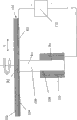
Figure 1A shows the schematic diagram according to the exemplary semiconductor structure of an embodiment.Exemplary semiconductor structure comprises the dielectric layer with groove area and non-groove area, the virtual architecture that forms and the metal that forms in non-groove area in non-groove area.Particularly, exemplary semiconductor structure comprises the dielectric layer 151 with groove area 151r and non-groove area 151n.Groove area 151r has been filled with metal level to form interconnection line 140.In addition, virtual architecture 130 has added non-groove area 151n and the interconnection line 140 adjacent with groove area 151r to.
In the exemplary configurations shown in Figure 1A, and on every side configuration virtual architecture adjacent with the interconnection line that in dielectric layer 151, forms 140.Yet, can be arranged in a plurality of positions according to applying virtual structure 130 with respect to interconnection line, comprise between each semiconductor element (dice) between the interconnection line 140, on the wafer etc.In addition, according to specific application and specific electrobrightening technology, can change the structure of virtual architecture 130 in many ways, for example density, spacing, shape etc.
Figure 1B shows the profile corresponding to the semiconductor structure of the line B-B line of Figure 1A.In this exemplary embodiment, patterned dielectric layer 151 is formed on the surface of semiconductor substrate layer 102.Patterned dielectric layer 151 comprises each groove that defined interconnection or the groove area 151r of line.Dielectric layer 151 comprises that also part is used for the non-groove area 151n of isolated interconnection line.Virtual architecture 130 is formed among the non-groove area 151n of dielectric layer 151.Metal level 104 can form structurally then, comprises virtual architecture 130 and non-groove area 151n and groove area 151r.Yet metal level 104 electrobrightenings are positioned at groove area 151r and virtual architecture 130 to non-groove area 151n so that metal level 104, as shown in the figure.By on groove area 151r, producing more constant current density and polishing speed, be arranged on the fluctuation that virtual architecture 130 among the non-groove area 151n of dielectric layer 151 has reduced the polishing speed of electrolyte.
By known patterning process deposit and patterned media layer 151 routinely, known patterning process for example is photomask, photoetching, micro-lithography etc.Can use the deposition process of any routine on substrate layer 102, to form dielectric layer 151, for example chemical vapor deposition, spin coating etc.Should be appreciated that dielectric layer 151 also can be formed on the layer that formed in the past.Dielectric layer can be for example silicon dioxide (SiO2).Often need to select to have the dielectric layer material of low-k, be called low " k " value material usually.This low-k materials comprises fluoridizes (flourinated) silicate glass, polyimides, fluorinated polyimide, mixtures, siloxanes, organic polymer, [Alpha]-C:F, the silica (silca) of Si-O-C, Parylene/fluohnated parlyene, polytetrafluoroethylene (polyterafluoroethylene), nanoporous, the organic substance of nanoporous etc.Usually, low k value material (that is, approximately less than 3.0) provides better electricity to isolate between interconnection line by capacitive coupling and " the crosstalking " that reduces between the adjacent lines.
Can be by any known method barrier layer 154 on dielectric layer, for example, chemical vapor deposition (CVD), physical vapor deposition (PVD), atomic layer deposition (ALD) etc., thus the barrier layer has covered the whole patterned dielectric layer that comprises groove and via sidewall.After deposited metal 104 subsequently, barrier layer 154 is used for preventing that metal (for example, copper) is diffused in the dielectric layer 151.Any metal diffusing is to the dielectric layer 151 interior performances that can reduce dielectric layer 151.Barrier layer 154 can be formed by any suitable electric conducting material that can prevent metal diffusing, for example, and titanium, tantalum, tungsten, titanium nitride, tantalum nitride, tungsten nitride or other suitable metal.In some applications, can omit barrier layer 154.For example, if dielectric material is enough to keep out the diffusion of metal level 104,, then can omit barrier layer 154 if the diffusion of perhaps any metal level 104 can not produce negative influence to the performance of semiconductor device.
If electroplated metal layer 104 on dielectric layer 151 subsequently for example, then deposit inculating crystal layer usually.Inculating crystal layer be generally metal level 104 can electroplate thereon metal or the thin layer of other electric conducting material.
If do not need the barrier layer, so in deposited metal 104 on the surface on barrier layer 154 or on the dielectric layer 151.Can pass through PVD, CVD, ALD, plating, chemical plating or any other method deposited metal 104 easily.Metal level 104 is, for example, and copper or other suitable electric conducting material, for example, aluminium, nickel, chromium, zinc, cadmium, silver, gold, rhodium, palladium, platinum, tin, lead, iron, indium or the like.In addition, metal level 104 can comprise the alloy of any these materials.
Following introduction comprises the additional example virtual structure that can be used for reducing polishing speed fluctuation in the electrobrightening technology.For helping the introduction of exemplary embodiment, illustrate to comprise the several exemplary structure that for example can cause the fluctuation of current density and polishing speed.Exemplary configurations is not exhaustive or qualification to the structure that can be used for virtual architecture.
Fig. 2 A shows the exemplary cross sectional view that can be used for the electrobrightening device of electrolysis polishing metal layer 104 from the semiconductor wafer 100.Semiconductor wafer 100 can comprise substrate layer 102.Substrate layer 102 for example comprises silicon and/or other various semi-conducting materials, and for example GaAs depends on specific application.
The nozzle of electrobrightening device makes the liquid stream of electrolyte 106 spray to the part surface of metal level 104.Electrolyte 106 comprises any liquid easily, for example phosphoric acid, orthophosphoric acid (H
2PO
4) etc.For example, in one embodiment, electrolyte 106 is orthophosphoric acid, has the concentration between about 60 percentage by weights and about 85 percentage by weights.In addition, electrolyte 106 can comprise for example ethylene glycol of 10 to 40 percentage by weights.Yet, should be appreciated that the concentration and the component that can change electrolyte 106 according to specific application.
When the stream with electrolyte 106 was sprayed onto on the metal level 104, power supply 112 was provided to the electrode 108 (negative electrode) of setting in the nozzle 110 and the electrode (anode) on the metal level 104 with opposite electric charge.Power supply 112 for example can be constant electric current or constant voltage mode work.When power supply 112 is arranged to make electrolyte 106 lotus positive electricity with respect to metal level 104, remove the metal ion of metal level 104 from the surface.In this way, that part of metal level 104 of the liquid stream of electrolyte 106 liquid stream electrobrightening contact electrolyte 106.
In addition, shown in Fig. 2 A, rotation wafer 100 also moves to the position of whole surface in the liquid stream of electrolyte 106 of metal level 104 along axle X, and electrobrightening surface equably.For example, by 100 while of rotation wafer translation wafer 100 in directions X, electrolyte 106 forms spiral path along the surface of metal level 104.Alternatively, fixed wafer 100 still, and moving nozzle 110 is applied to the liquid stream of electrolyte 106 part that needs of metal level 104 simultaneously.In addition, can mobile wafer 100 and nozzle 110 the liquid stream of electrolyte 106 is applied to the part that needs of metal level 104.The U.S. patent No.09/497 that the exemplary illustration of electrobrightening was submitted to referring on February 4th, 2000, in 894, exercise question is METHODS AND APPARATUSFOR ELECTROPOLISHING METAL INTERCONNECTIONS ONSEMICONDUCTOR DEVIES, and its whole contents here is incorporated herein by reference.
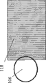
Fig. 2 B shows the vertical view of the exemplary configurations of the tube core 118 that forms on semiconductor wafer 100.Each tube core 118 is included in groove or the line (Figure 1B) that forms in the following dielectric layer 151, is shown as vertical line here.Often when electrobrightening technology begins, cover the whole surface (Fig. 2 A) of the wafer 100 of the trench area that comprises tube core 118 with metal level 104.Path 10 shows the liquid stream of electrolyte 106 in the mobile path of wafer 100 on every side.
When beginning electrobrightening technology, in the entire profile of liquid stream, the surface of that part of wafer 100 of the liquid of electrolyte 106 stream contact has the metal of approximate same amount.Remove metal level 104 (Fig. 2 A) to expose the metal level 104 (Fig. 2 A) that electricity is isolated in non-groove area and the groove by the liquid stream of electrolyte 106.Thus, owing to that part of metal level 104 (Fig. 2 A) in the trench area stays, therefore according to the position of stream, the liquid of electrolyte 106 flows the metals that part of wafer 100 that contacts can have different amounts.
For example, in Fig. 2 B, the liquid stream of electrolyte 106 is positioned on the tube core 118.Because metal level 104 (Fig. 2 A) electroplated, so the non-groove area of tube core 118 metal that has is less than trench area.Because the liquid of electrolyte 106 stream 10 moves along the path, therefore in any given position, the amount of trench area and non-groove area, wafer 100 surfaces are gone up the areas that metal levels 104 (Fig. 2 A) cover and are changed in the liquid of electrolyte 106 stream thus.
Cause " overall load effect " (globalloading effect) of being called here owing to remove in the liquid stream of the electrolyte 106 that metal causes this variation of metallic area on the wafer 100 from the zone between the tube core 118.As following more detailed introduction, the overall load effect can cause that the polishing speed of electrolyte fluctuates near the edge of trench area.
Fig. 3 A flows in the overall load effect that moves to the position that covers tube core 118 on the groove area fully from non-groove area with tube core 118 position adjacent to the liquid that 3D shows along with electrolyte 106.As shown in Figure 3A, if power supply 112 (Fig. 2 A) moves in constant current-mode, the current density in the liquid of electrolyte 106 stream is lower so, is because the metal level 104 (Fig. 2 A) in the non-groove area is even basically.Current density any one specific part in liquid stream in the liquid stream of electrolyte 106 is not bigger, and this is because even basically in the non-groove area of wafer 100 (Fig. 2 A) by the surface of electrobrightening.
The liquid stream that Fig. 3 B shows electrolyte 106 reaches tube core 118 and begins electrobrightening tube core 118 leftmost groove or lines as liquid stream.The part liquid of the liquid stream of electrolyte 106 flows the interior metal of trench area of present electrobrightening tube core 118.Current density on the tube core 118 in that part of liquid stream of the liquid of electrolyte 106 stream is with respect to the current density increase of flowing among Fig. 3 A and reach maximum.Current density in this part of liquid stream, increase be since with tube core 118 outside non-groove area in barrier layer 154 (Figure 1B) or dielectric layer 151 (Figure 1B) compare the easier polishing of the metal in the trench area (resistance is littler).
The liquid that Fig. 3 C shows electrolyte 106 flows the zone greatly of further moving and beginning electrobrightening tube core 118 as liquid stream on tube core 118.Along with the present metallic area increase that covers of the liquid stream of electrolyte 106, the current density of electrolyte 106 reduction on the trench area among Fig. 3 C.When the liquid stream of electrolyte 106 moved on the tube core 118 fully, current density further was reduced to the current value among Fig. 3 D.Current density will remain on this steady state value, and stream is retained on the tube core 118 fully simultaneously.Along with the liquid stream of electrolyte 106 moves on the tube core 118, metallic region increases, the current density fluctuation of stream.The variation of the interior current density of the liquid of that part of electrolyte 106 stream causes the polishing speed of metal level to change on the tube core 118.Particularly, current density and polishing speed change the edge occur in tube core 118 or near.
The liquid stream that Fig. 4 A shows along with electrolyte 106 moves the result of the respective change of the polishing speed of current density change and electrolyte stream on tube core 118.Particularly, Fig. 4 A shows as Fig. 3 A to the leftmost groove 420,422,424 and 426 that flows the tube core 118 (Fig. 3 A) that has polished shown in the 3D with the liquid of electrolyte 106.As shown in the figure, metal is polished to bigger degree in leftmost groove 420.Excessive polishing in the groove 420 is called metal groove.Along with constantly reducing away from the metal groove in the remaining groove 422,424 in the edge of tube core 118 and 426, this is because along with liquid stream mobile polishing speed on tube core 118 reduces.Therefore, the groove on groove 426 the right has less metal groove, and this is because when liquid stream was positioned on the tube core 118 fully, current density and polishing speed can rapid fluctuations.
Introduce to 3D with reference to figure 3A as top, along with electrolyte stream moves on tube core 118, when the Far Left of tube core 118 only is in liquid and flows down face, current density and polishing speed maximum.Be in along with increasing tube core under the path of liquid stream, current density reduces.Therefore, metal groove in the groove on groove 420 the right reduce up to reach with the edge near compare and change less horizontal plane, when liquid stream was on the tube core 118 fully, the fluctuation in the current density was less.Groove 420,422,424 and 426 metal groove and the difference in height of filling metal can cause the electric guided wave of metal wire moving and influence the performance of semiconductor device negatively.
Fig. 4 B shows exemplary virtual architecture.As shown in the figure, virtual architecture 428,430 and 432 has been included near the edge and ragged edge groove 420 of tube core 118.By producing more constant current density and polishing speed on the groove of tube core 118, virtual architecture 428,430 and 432 is provided with to such an extent that reduced the polishing speed fluctuation of electrolyte stream near ragged edge groove 420.Current density mainly fluctuates on virtual architecture now, and metal groove will occur in virtual architecture 428,430 and 432.When liquid stream reaches groove 420, great majority or all liquid stream will be on virtual architecture 428,430 and 432, and the current density of liquid stream will keep constant relatively on groove.Virtual architecture will reduce the metal groove of finding in the groove of Fig. 4 A and produce more uniform groove thus.
Virtual architecture 428,430 and 432 can comprise with its on to be deposited with the material of dielectric layer of metal level identical, perhaps can comprise other suitable material that is suitable for application-specific.If virtual architecture 428,430 and 432 is by forming with the dielectric layer identical materials, virtual architecture 428,430 and 432 can form simultaneously with groove 420,422,424 and 426 (Fig. 4 A) so.When metal level was layered on the groove 420,422,424 and 426 (Fig. 4 A) then, metal level can be layered on virtual architecture 428,430 and 432.Alternatively, can before or after forming, groove 420,422,424 and 426 form virtual architecture 428,430 and 432.If virtual architecture 428,430 and 432 is formed by the material different with dielectric layer, for example copper or other metal, so by any technology easily can deposition materials then composition form the structure that needs of virtual architecture 428,430 and 432.In addition, virtual architecture 428,430 and 432 can be the groove of physical dimension that is similar to the groove 420 of tube core 118, perhaps alternatively can be other shape and size, and this depends on uses or electroplate character.Introduce multiple additional shape and structure below.
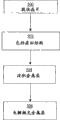
Fig. 5 is the flow chart of illustrative metal mosaic technology.Wafer with groove and non-groove area is provided in the square 500.Be provided at that patterned dielectric layer can limit groove and non-groove area on the wafer.In addition, after the technology that is processed into single semiconductor device finished, wafer can be divided into each tube core.Virtual architecture can be included on the wafer in square frame 502.Virtual architecture can be positioned at outside each tube core, and is perhaps as described below, in each tube core adjacent with each line or high density graph.In square frame 504, can deposited metal, so that groove area and non-groove area in the metal level filled media layer.The electrobrightening metal level is removed metal level and isolated metal structure either with the non-groove part from dielectric layer in square frame 506 then.Be used for the material of illustrative metal mosaic technology and material and the method that method can be any routine.
Should be appreciated that and to carry out a large amount of modifications to the technology shown in the flow chart.For example, in square frame 504, can add barrier layer and/or inculating crystal layer before the deposited metal.In addition, each square frame among Fig. 5 can comprise many technologies of clearly not introducing, for example shelters with etched wafer and forms virtual architecture and groove area.In addition, damascene process An can be applied to list and dual damascene applications.
Fig. 6 shows the schematic diagram of the exemplary virtual architecture adjacent with singulated dies 118.As shown in the figure, with tube core 118 adjacent areas in, formed virtual architecture.In this embodiment, virtual architecture 630 is arranged in from each limit of tube core 118 zone of extended distance " a " at least.Select more than or equal to distance D (that is, a〉D) apart from a, wherein D equals the diameter of the liquid stream of electrolyte 106.The liquid that virtual architecture 630 is used to keep pass the electrolyte 106 of tube core 118 flows geostationary current density.The density that the ratio in space can be regulated virtual architecture 630 between size by changing virtual architecture 630 and the virtual architecture.Can change the size and dimension of virtual architecture 630 according to specific application.Virtual architecture 630 also can be used to be configured to tube core 118 continuous line or groove on every side.In addition, should be appreciated that and to use any amount of virtual architecture 630 according to using.
Fig. 7 shows the schematic diagram according to the adjacent example virtual structure of another embodiment and four tube cores 118.The similar of Fig. 7 is in Fig. 6, and except in this embodiment, the area of the virtual architecture adjacent with four tube cores 118 is not greater than or equal to the diameter D of the liquid stream of electrolyte 106.Range of a signal b and c equal level and the vertical interval between the adjacent tube core 118 respectively.Along with the liquid of electrolyte 106 stream moves to the next one from a tube core 118, the groove structure of each tube core 118 will be shared the electric current of liquid stream.Therefore, by between tube core 118, adding virtual architecture 630, can keep the current density of approximately constant with distance b and/or c less than D.
Should be realized that can the technology of ground shown in Fig. 5 and Fig. 6 and shown in exemplary configurations carry out various modifications.For example, the virtual architecture among Fig. 6 and 7 has the shape except that square, the shape of introducing with reference to figure 17A-17AA for example, and can further be the one or more lines adjacent with tube core 118.
Can be similar to the overall load effect by the amount external effect during electrobrightening, the regional area that occurs in tube core except it is called " partial load effect " here.When from tube core on structure adjacent areas (field) or the partial load effect can take place during non-groove area polishing metal.Along with electrobrightening technology is removed metal from the non-groove area of tube core, the amount of metal reduces.If carry out electrobrightening technology in constant-current mode, the electric current in the electrolyte stream accumulates on the residue trench region of tube core so, can cause low-density graph area and high density graph district high current density at the interface.High current density on the trench area can cause the end-point detection difficulty, and the polishing of crossing that causes the interior metal groove of groove.
In addition, if the partial load effect can take place with constant-voltage mode work in electrobrightening technology so.With reference to figure 2A, the electric current that flows through the electrobrightening device has four main resistance sources between negative electrode and anode again.First resistance source R1 is the resistance of the liquid stream of electrolyte 106.Second resistance source R2 resistance at the interface between the liquid stream of the surface of wafer 100 and electrolyte 106.The 3rd resistance source R3 is for being polished to the resistance of that part of wafer 100 of electrode from the edge of wafer 100.Resistance at the interface between the liquid stream that the 4th resistance source R4 is injector electrode 108 (negative electrode) and electrolyte 106.Flow through the following expression of electric current I of system with constant-voltage mode:
I=V/(R1+R2+R3+R4)
Wherein V is the polishing voltage of power supply 112.
Along with glossing is removed metal from non-groove area, it is because the amount minimizing of metal area in the liquid stream that second resistance R 2 reduces.Yet the electric current in the liquid of electrolyte 106 stream depends on all-in resistance R (R1+R2+R3+R4), and along with metallic area reduces, all-in resistance R is along with reduce pro rata (that is, quick) of resistance R 2 reduces.Therefore, because the proportional reduction of electric current is less than the minimizing in the metal area, therefore current density and polishing speed increase on remaining trench area.The metal valley of introducing more than this effect produces in trench area.For this effect of low-density graph area lay special stress on the tube core.
Fig. 8 shows the schematic diagram according to the example virtual structure of the adjacent setting of each line on the density regions of an embodiment and tube core.Line 840a is a low-density figure on the tube core to 840j.Virtual architecture 630 be provided with near and around low pattern density district.Virtual architecture 630 has increased the averag density of metal structure in the different density regions of tube core.The electric current that the averag density increase of metal structure has reduced electrolyte stream changes and has reduced metal groove.In addition, in order to reduce line 840a to the electric capacity between the 840j, separation line 840a to the space of 840j and virtual architecture 630 for example more than or equal to the minimum space that in the design rule of dielectric layer, allows, twice or for example trebly greater than the minimum space of structure Design rule.In other embodiments, according to application space a and b even can be bigger.In addition, can change the quantity and the shape of virtual architecture according to concrete application.
Fig. 9 shows the schematic diagram according to the example virtual structure of the adjacent setting of each line on the density regions of another embodiment and tube core.In the present embodiment, line 940a is arranged in the density regions of tube core to 940g, and also comprises the space between each line, for example space between line 940a and the 940b.Virtual architecture 630 and line 940a be to the adjacent setting of 940g, and also in the space between adjacent each line, the space between for example space between 940a and the 940b, and 940e and the 940f.Virtual architecture 630 is placed in the space between adjacent each line, to reduce the partial load effect in these density regions.Particularly, virtual architecture 630 has reduced the electric current gathering, and promptly the online 940a of current density concentration is to 940b.When the distance between line 940a and the 940b became big, line 940a was called shielding wire or isopleth (isoline) usually.
In electroplating technology, be electroplated onto in the high density composition district of tube core locally at metal level, can take place to be called here " bulge effect ".Bulge effect is the zone of electroplating crossing of particularly taking place on the zone at the high density composition of tube core during the electroplating technology or the plane raises.Bulge effect comprises the inclination or the non-horizontal surface zone of metal level on the trench area edge.Non-horizontal surface can make the complanation of metal surface become difficult.Particularly, when the electrobrightening tilting zone, groove can be present in each line vertical end place or near, also be present in each line high-density region the most external line edge or near.
Figure 10 A shows the process chart of exemplary groove structure to 10F, demonstrates bulge effect and gained groove near the longitudinal edge of each line.Figure 10 A shows the sectional view of the depressed area of the groove that forms in dielectric layer 1060.Dielectric layer 1060 can be by forming with the above similar material of introducing at Figure 1A, and for example silicon dioxide and other advanced low-k materials depend on concrete application.Also can be deposited on the dielectric layer 1060 according to using barrier layer and/or inculating crystal layer 1070.Barrier layer and/or inculating crystal layer 1070 also can be by forming with the above similar material of introducing at Figure 1A.Figure 10 B shows in dielectric layer 1,060 three grooves forming or the vertical view of line 1061,1062 and 1063.
Then shown in profile among Figure 10 C and the 10D and vertical view difference, with this structure of metal level 1064 plating.Shown in Figure 10 C and 10D, crossing on the groove electroplated and produce a protuberance in high density composition district.The height of protuberance is shown as h3, is the difference between the height h2 of metal lining in the not composition district of the height h1 of metal lining in the not composition district of dielectric layer 1060 and dielectric layer 1060.The non-horizontal zone of metal level 1064 is shown as 1066.Near from h1 to the transition of h3 plating the edge of online 1061,1062 and 1063 (Figure 10 A and 10B) distance shows with w1 and w2.
Figure 10 E and 10F show metal level 1064 electrobrightening to dielectric layer 1060 to isolate the structure after 1061,1062 and 1063.Electrobrightening metal 1064 with non-horizontal zone of metal level 1066 can produce metal groove in online 1061,1062 and 1063.Opposite with the chemico-mechanical polishing of at first polishing the highest region territory, electrobrightening has polished the exposing surface of metal level 1066 with substantially the same speed and irrelevant with different height.This causes online 1061,1062 and 1063 end or neighbouringly is the edge of the outside line of line 1061 and 1063 or the metal level 1064 that near generation has groove equally at this moment.Groove can show as by near height in the middle of difference in height h4 in the metal at line edge and the metal level 1064.Introduce at overall load effect and partial load effect as top, the electricity that metal groove causes metal loss and reduced metal wire is led.
Figure 11 A shows according to exemplary each line of an embodiment and the figure of virtual architecture to 11C.Figure 11 A is the vertical view that is similar to the structure that comprises line 1161,1162 and 1163 that Figure 10 A forms, except virtual architecture 630 is provided with near vertical end of line 1161,1162 and 1163 and adjacent with the outside line of line 1161 and 1163.Virtual architecture 630 is used for the nonplanar massif (referring to Figure 10 C) that tilts is extended to the line that line 1161,1162 and 1163 are set or the zone of array area outside.By add virtual architecture 630 can reduce or eliminate vertical end place of each line of array or near and the edge of the outside line of array or near metal groove.
Figure 11 B and 11C show the profile of the virtual architecture 630 that comprises line 1163 and vertical end place.Shown in Figure 11 B, the non-horizontal zone 1164 of metal level 1164 is positioned on virtual architecture 630 and the dielectric layer 1160 now.In Figure 11 C metal level 1164 by electrobrightening after, the metal grooves in the line 1163 reduce or eliminate.
Can be according to the quantity of use regulating virtual architecture 630 and width to reduce any metal groove in the line 1163.Virtual architecture 630 can be configured to the row adjacent with line 1161,1162 and 1163 shown in Figure 11 A, perhaps alternatively more than row.Can select the quantity and the structure of virtual architecture 630 according to the characteristic of protuberance, for example the slope of Long Qi height or non-horizontal zone.By adjusting defined metal wire 1161,1162 and 1163 and virtual architecture 630 between the space a in space and the structure that b can operate virtual architecture 630 equally.The minimum space that this space allows more than or equal to the design rule that is used for dielectric layer usually.At this moment, virtual architecture 630 is shown as the degree of depth that has and equals the square of the line 1161,1162 and 1163 degree of depth, but should be realized that virtual architecture 630 can be configured to the Any shape or the degree of depth.Therefore can operate the multiple attribute of virtual architecture 630 in many ways.
Figure 12 shows according to an embodiment and high-density lines or the adjacent example virtual structure of array.In the present embodiment, adjacent and with line 1261,1262 and 1263 around continuous metal wire 1231 is set.By the non-horizontal zone of the inclination that makes protuberance move away from introduce above have the line of Figure 11 A to the virtual architecture 630 of 11C, continuous metal wire 1231 is used for the metal groove of anti-principal vertical line 1261,1262 and 1263.Should be appreciated that and to use a plurality of metal wires 1231 or extra virtual architecture, for example can connect metal wire 1231 among Figure 11 A.In addition, metal wire 1231 can comprise copper, aluminium, nickel, chromium, zinc, cadmium, silver, gold, rhodium, palladium, platinum, tin, lead, iron, indium etc.In addition, metal wire 1231 can comprise the alloy that these materials are any.
Figure 13 shows the example virtual structure according to another embodiment.Example semiconductor device shown in Figure 13 is very similar to the example semiconductor device shown in Figure 11 A, only is added on except virtual architecture 1330 near the longitudinal end of each line 1361,1362 and 1363.In addition, the virtual architecture 1330 of Figure 13 has been added between the longitudinal end of each line 1361,1362 and 1363.As previously mentioned, should be appreciated that the virtual architecture that can use any amount of virtual architecture and multiple structure according to concrete application.
Figure 14 shows the example virtual structure according to another embodiment.Example semiconductor device shown in Figure 14 is very similar to the example semiconductor device shown in Figure 13, except virtual architecture 1431 by square with shown in Figure 13 each or put relative continuous line and form.Yet, should be appreciated that any combination that can use line and each structure according to using.
Also virtual architecture can be added to a plurality of effects of semiconductor device here to reduce to introduce.For example, as shown in figure 15, to 1540j, virtual architecture has been added on two zoness of different of tube core to reduce partial load effect and bulge effect for line 1540a.Virtual architecture 1530 added to high-density lines or array adjacent areas to reduce bulge effect.Virtual architecture 1530 reduced above at Figure 11 A introduce each line place or near metal groove.In addition, virtual architecture 1532 can add opening (open) or density regions to equally to increase average pattern density and to avoid the partial load effect.Virtual architecture 1532 has reduced the current density on each line, this current density can cause during the above electrobrightening technology of introducing at Fig. 8 the place, end of each line or near cross polishing.
Figure 16 shows the example semiconductor device according to another embodiment, has reduced partial load effect and bulge effect for line 1640a to 1640g.Example semiconductor device shown in Figure 16 is similar to the example semiconductor device shown in Figure 15, except virtual architecture 1530 adds between online 1640a and the 1640b and between 1560e and the 1640f.
In addition, the example semiconductor device shown in Figure 15 and 16 comprise equally with semiconductor wafer on the adjacent virtual architecture of tube core to have reduced the overall load effect.
Figure 17 A shows the various exemplary shape that is used for forming virtual architecture here according to any exemplary embodiment of introducing on semiconductor device to 17AA.Particularly, can use rectangle, circle, ellipse, triangle, trapezoidal, octagon, hexagon, pentagon etc.Yet should be appreciated that other shape that can use Figure 17 A not illustrate in the 17AA according to specific application forms virtual architecture of the present invention.In addition, virtual architecture can be configured to have the line (for example referring to Figure 12 and 14) of different shape, comprises multiple cross sectional shape.Virtual architecture can be formed by different materials, for example silicon dioxide and other other suitable material with low-k form, for example fluorinated silicate glass, polyimides, fluorinated polyimide, mixtures, siloxanes, organic polymer, [Alpha]-C:F, the silica of Si-O-C, Parylene/fluohnated parlyene, polytetrafluoroethylene, nanoporous, the organic substance of nanoporous etc.As mentioned above, in some cases, virtual architecture can be by forming with the dielectric layer identical materials.Virtual architecture can be formed by following metal, for example: copper, aluminium, nickel, chromium, zinc, cadmium, silver, gold, rhodium, palladium, platinum, tin, lead, iron, indium etc.In addition, virtual architecture can be by any alloy of these materials.
Provide above detailed description to introduce exemplary embodiment rather than determinate.Obviously multiple modification and distortion can be arranged within the scope of the invention to those skilled in the art.For example, add to wafer be used to reduce the overall load effect virtual architecture can be used for partial load effect, bulge effect or the two virtual architecture and be used in combination.In addition, specifically the shape and the structure of the example virtual structure of introduction can alternatively be used to solve any of these effect or any other reason according to application to be used to reduce integral body, part or bulge effect here.Therefore, the present invention is defined by the claims rather than the explanation here.
Claims (65)
1. semiconductor structure comprises:
Be positioned at groove area on the dielectric layer and the metal level on non-groove area and the virtual architecture; And
Be positioned at the dielectric layer under the described metal level, comprise:
The figure of groove and non-groove area, wherein from non-groove area electrobrightening metal level and filling groove district, forming a plurality of interconnection lines, and
A plurality of virtual architectures, wherein virtual architecture is positioned at the non-groove area of dielectric layer.
2. according to the semiconductor structure of claim 1, the part of wherein said a plurality of virtual architectures is arranged to be less than or equal to apart from the distance of groove area the diameter of the electrolyte stream that is produced by the electrobrightening device.
3. according to the semiconductor structure of claim 1, wherein the part of a plurality of virtual architectures is arranged to adjacent with at least one of described a plurality of interconnection lines.
4. according to the semiconductor structure of claim 1, it is adjacent with vertical end of described a plurality of interconnection lines that wherein said a plurality of virtual architectures are arranged to.
5. according to the semiconductor structure of claim 1, the part of wherein said a plurality of virtual architectures is arranged between two of described a plurality of interconnection lines at least.
6. according to the semiconductor structure of claim 1, wherein said a plurality of virtual architectures are arranged to adjacent with the high density area of described a plurality of interconnection lines.
7. according to the semiconductor structure of claim 1, the part that wherein said a plurality of virtual architectures are arranged to a plurality of interconnection lines described in the low density area with described a plurality of interconnection lines is adjacent.
8. according to the semiconductor structure of claim 1, wherein said a plurality of virtual architectures are arranged to adjacent with the both sides of shielding wire.
9. according to the semiconductor structure of claim 1, the part of wherein said a plurality of virtual architectures is arranged to the distance of the described groove area of distance more than or equal to the minimum range between two groove areas that design rule allowed.
10. according to the semiconductor structure of claim 1, the part of wherein said a plurality of virtual architectures is arranged at least twice of the distance of the described groove area of distance greater than minimum range between two groove areas of design rule permission.
11. according to the semiconductor structure of claim 1, wherein said a plurality of virtual architectures are with metal filled.
12. according to the semiconductor structure of claim 1, wherein said a plurality of virtual architectures are the line of adjacency.
13. according to the semiconductor structure of claim 1, wherein said a plurality of virtual architectures comprise metal wire.
14. according to the semiconductor structure of claim 1, the width of wherein said virtual architecture is more than or equal to the width of described a plurality of interconnection lines.
15. according to the semiconductor structure of claim 1, the density of wherein said a plurality of virtual architectures is more than or equal to the density of described a plurality of interconnection lines.
16. according to the semiconductor structure of claim 1, wherein said a plurality of virtual architectures be evenly distributed in described a plurality of interconnection line adjacent areas in.
17., wherein dispose the depression of described a plurality of virtual architecture with the metal level that reduces on described a plurality of interconnection lines, to form according to the semiconductor structure of claim 1.
18., wherein dispose described a plurality of virtual architecture to increase to the averag density of the metal structure in the described semiconductor structure of small part according to the semiconductor structure of claim 1.
19., wherein described metal level electrobrightening is isolated a plurality of described groove areas with electricity according to the semiconductor structure of claim 1.
20., also comprise the barrier layer that is arranged between described metal level and the described dielectric layer according to the semiconductor structure of claim 1.
21., also comprise the inculating crystal layer that is arranged between described metal level and the described dielectric layer according to the semiconductor structure of claim 1.
22. a semiconductor structure comprises:
A plurality of semiconductor elements, wherein a plurality of semiconductor elements comprise:
Dielectric layer with a plurality of grooves, and
By electrobrightening and filling groove to form the metal level of interconnection line; And
A plurality of virtual architectures with the adjacent formation of a plurality of semiconductor elements.
23. according to the semiconductor structure of claim 22, the part of wherein said a plurality of virtual architectures is arranged to be less than or equal to apart from the distance of the described groove of part the diameter of the electrolyte stream that is produced by the electrobrightening device.
24. according to the semiconductor structure of claim 22, wherein said a plurality of virtual architectures are with metal filled.
25. according to the semiconductor structure of claim 22, wherein said a plurality of virtual architectures are filled with copper.
26. according to the semiconductor structure of claim 22, wherein said metal level is formed on tube core and the virtual architecture simultaneously.
27. according to the semiconductor structure of claim 22, wherein said a plurality of virtual architectures are the line of adjacency.
28. according to the semiconductor structure of claim 22, wherein said a plurality of virtual architectures comprise the metal wire with the adjacent formation of at least a portion of described a plurality of grooves.
29. according to the semiconductor structure of claim 22, wherein said a plurality of virtual architectures be arranged on the semiconductor element adjacent areas in, the distance that described a plurality of virtual architectures extend from semiconductor element is more than or equal to the smaller the following distance:
Equal the distance of the diameter of the electrolyte stream that produces by the electrobrightening device, or
Equal two distances between the adjacent tube core.
30. according to the semiconductor structure of claim 22, the width of wherein said a plurality of virtual architectures is more than or equal to the width of described a plurality of grooves.
31. according to the semiconductor structure of claim 22, the distance that wherein separates described a plurality of virtual architectures is more than or equal to the minimum range that separates described a plurality of grooves.
32. according to the semiconductor structure of claim 22, wherein said a plurality of virtual architectures be evenly distributed in described a plurality of tube core adjacent areas in.
33., wherein dispose described a plurality of virtual architecture with the depression at least a portion groove that reduces described a plurality of grooves according to the semiconductor structure of claim 22.
34., wherein dispose described a plurality of virtual architecture to increase to the averag density of the metal structure in the small part semiconductor wafer according to the semiconductor structure of claim 22.
35., wherein described metal level electrobrightening is isolated described a plurality of groove with electricity according to the semiconductor structure of claim 22.
36., also comprise the barrier layer that is arranged between described metal level and the described dielectric layer according to the semiconductor structure of claim 22.
37., also comprise the inculating crystal layer that is arranged between described metal level and the dielectric layer according to the semiconductor structure of claim 22.
38. the preparation method of a semiconductor structure comprises:
Be positioned at groove area on the dielectric layer and the metal level on non-groove area and the virtual architecture,
Form dielectric layer under described metal level, dielectric layer comprises groove area and non-groove area;
In non-groove area, form a plurality of virtual architectures;
Form metal level with blanket dielectric layer and virtual architecture; And
The electrobrightening metal level is to expose non-groove area.
39., wherein form metal level and comprise deposited metal according to the method for claim 38.
40., wherein form metal level and comprise electroplated metal layer according to the method for claim 38.
41. according to the method for claim 38, the width that each virtual architecture of wherein said a plurality of virtual architectures has is more than or equal to the width of described groove area.
42. according to the method for claim 38, each virtual architecture of wherein said a plurality of virtual architectures is spaced from each other equal distance.
43. according to the method for claim 38, the minimum range between wherein said virtual architecture and the described groove area is more than or equal to the design rule of groove area.
44. according to the method for claim 38, wherein said groove area is a groove, forms interconnection line when filling with metal level.
45. according to the method for claim 38, wherein said a plurality of virtual architectures are with metal filled.
46. according to the method for claim 38, wherein the effect of electrobrightening comprises the surface that electrolyte stream is guided to described metal level.
47. the preparation method of an interconnection structure comprises:
Form dielectric layer, wherein to the dielectric layer composition to be used to form interconnection line;
Form and the adjacent a plurality of virtual architectures of interconnection line that will form;
Form metal level to cover patterned dielectric layer and virtual architecture; And
The electrobrightening metal level is with the isolated interconnection line.
48., wherein form metal level and comprise deposited metal according to the method for claim 47.
49., wherein form metal level and comprise electroplated metal layer according to the method for claim 47.
50. according to the method for claim 47, the width that each virtual architecture of wherein said a plurality of virtual architectures has is more than or equal to the width of described interconnection line.
51. according to the method for claim 47, each of wherein said a plurality of virtual architectures is spaced from each other equal distance.
52. according to the method for claim 47, the minimum range between wherein said virtual architecture and the described interconnection line is more than or equal to the design rule of groove area.
53. according to the method for claim 47, wherein said a plurality of virtual architectures are with metal filled.
54. according to the method for claim 47, wherein the effect of electrobrightening comprises the surface that electrolyte stream is guided to described metal level.
55. the preparation method of a semiconductor structure comprises:
On semiconductor wafer, form a plurality of tube cores, wherein form each tube core and comprise:
Formation has the dielectric layer of groove area and non-groove area;
On dielectric layer, form metal level and filling groove district;
In the non-groove area of dielectric layer, form at least one virtual architecture; And
The electrobrightening metal level is to expose non-groove area.
56., wherein form metal level and comprise deposited metal according to the method for claim 55.
57., wherein form metal level and comprise electroplated metal layer according to the method for claim 55.
58. according to the method for claim 55, the width that each virtual architecture of wherein said a plurality of virtual architectures has is more than or equal to the width of described groove area.
59. according to the method for claim 55, each of wherein said a plurality of virtual architectures is spaced from each other equal distance.
60. according to the method for claim 55, the minimum range between wherein said virtual architecture and the described groove area is more than or equal to the design rule of groove area.
61. according to the method for claim 55, wherein when filling with metal level, described groove area forms interconnection line.
62. according to the method for claim 55, wherein said a plurality of virtual architectures comprise metal.
63. according to the method for claim 55, wherein said a plurality of virtual architectures comprise and described dielectric layer identical materials.
64. according to the method for claim 55, wherein the effect of electrobrightening comprises the surface that electrolyte stream is guided to described metal level.
65. according to the method for claim 55, the distance that wherein said virtual architecture extends from tube core is more than or equal to the diameter of electrolyte stream or the distance between the adjacent tube core.
Applications Claiming Priority (2)
| Application Number | Priority Date | Filing Date | Title |
|---|---|---|---|
| US31461701P | 2001-08-23 | 2001-08-23 | |
| US60/314,617 | 2001-08-23 |
Publications (2)
| Publication Number | Publication Date |
|---|---|
| CN1547763A CN1547763A (en) | 2004-11-17 |
| CN100524644C true CN100524644C (en) | 2009-08-05 |
Family
ID=23220680
Family Applications (1)
| Application Number | Title | Priority Date | Filing Date |
|---|---|---|---|
| CNB028165098A Expired - Fee Related CN100524644C (en) | 2001-08-23 | 2002-08-16 | Dummy structures to reduce metal recess in electropolishing process |
Country Status (8)
| Country | Link |
|---|---|
| US (1) | US20040253810A1 (en) |
| EP (1) | EP1419523A4 (en) |
| JP (1) | JP2005501412A (en) |
| KR (1) | KR101055564B1 (en) |
| CN (1) | CN100524644C (en) |
| CA (1) | CA2456301A1 (en) |
| TW (1) | TW573324B (en) |
| WO (1) | WO2003019641A1 (en) |
Families Citing this family (10)
| Publication number | Priority date | Publication date | Assignee | Title |
|---|---|---|---|---|
| EP1505653A1 (en) | 2003-08-04 | 2005-02-09 | STMicroelectronics S.r.l. | Layout method for dummy structures and corresponding integrated circuit |
| US20050045993A1 (en) * | 2003-08-28 | 2005-03-03 | Sanyo Electric Co., Ltd. | Semiconductor device with concave patterns in dielectric film and manufacturing method thereof |
| US7074710B2 (en) * | 2004-11-03 | 2006-07-11 | Lsi Logic Corporation | Method of wafer patterning for reducing edge exclusion zone |
| JP5401135B2 (en) * | 2009-03-18 | 2014-01-29 | 株式会社ニューフレアテクノロジー | Charged particle beam drawing method, charged particle beam drawing apparatus and program |
| KR101067207B1 (en) * | 2009-04-16 | 2011-09-22 | 삼성전기주식회사 | A trench substrate and a fabricating method the same |
| US20130075268A1 (en) * | 2011-09-28 | 2013-03-28 | Micron Technology, Inc. | Methods of Forming Through-Substrate Vias |
| CN103692293B (en) * | 2012-09-27 | 2018-01-16 | 盛美半导体设备(上海)有限公司 | non-stress polishing device and polishing method |
| US8627243B1 (en) * | 2012-10-12 | 2014-01-07 | Taiwan Semiconductor Manufacturing Company, Ltd. | Methods for optimizing conductor patterns for ECP and CMP in semiconductor processing |
| WO2014082197A1 (en) * | 2012-11-27 | 2014-06-05 | Acm Research (Shanghai) Inc. | Method for forming interconnection structures |
| US11328992B2 (en) * | 2017-09-27 | 2022-05-10 | Intel Corporation | Integrated circuit components with dummy structures |
Citations (3)
| Publication number | Priority date | Publication date | Assignee | Title |
|---|---|---|---|---|
| US5885856A (en) * | 1996-08-21 | 1999-03-23 | Motorola, Inc. | Integrated circuit having a dummy structure and method of making |
| CN1264162A (en) * | 1999-02-13 | 2000-08-23 | 国际商业机器公司 | Virtual pattern for aluminium chemical polishing |
| US6232231B1 (en) * | 1998-08-31 | 2001-05-15 | Cypress Semiconductor Corporation | Planarized semiconductor interconnect topography and method for polishing a metal layer to form interconnect |
Family Cites Families (14)
| Publication number | Priority date | Publication date | Assignee | Title |
|---|---|---|---|---|
| JPS59182541A (en) * | 1983-04-01 | 1984-10-17 | Hitachi Ltd | Manufacture of semiconductor device |
| US5677244A (en) * | 1996-05-20 | 1997-10-14 | Motorola, Inc. | Method of alloying an interconnect structure with copper |
| US6017437A (en) * | 1997-08-22 | 2000-01-25 | Cutek Research, Inc. | Process chamber and method for depositing and/or removing material on a substrate |
| US6309956B1 (en) * | 1997-09-30 | 2001-10-30 | Intel Corporation | Fabricating low K dielectric interconnect systems by using dummy structures to enhance process |
| US6052375A (en) * | 1997-11-26 | 2000-04-18 | International Business Machines Corporation | High speed internetworking traffic scaler and shaper |
| TW396524B (en) * | 1998-06-26 | 2000-07-01 | United Microelectronics Corp | A method for fabricating dual damascene |
| US6395152B1 (en) * | 1998-07-09 | 2002-05-28 | Acm Research, Inc. | Methods and apparatus for electropolishing metal interconnections on semiconductor devices |
| US6709565B2 (en) * | 1998-10-26 | 2004-03-23 | Novellus Systems, Inc. | Method and apparatus for uniform electropolishing of damascene ic structures by selective agitation |
| US6259115B1 (en) * | 1999-03-04 | 2001-07-10 | Advanced Micro Devices, Inc. | Dummy patterning for semiconductor manufacturing processes |
| US6239023B1 (en) * | 1999-05-27 | 2001-05-29 | Taiwan Semiconductor Manufacturing Company | Method to reduce the damages of copper lines |
| US6459156B1 (en) * | 1999-12-22 | 2002-10-01 | Motorola, Inc. | Semiconductor device, a process for a semiconductor device, and a process for making a masking database |
| JP2002158278A (en) * | 2000-11-20 | 2002-05-31 | Hitachi Ltd | Semiconductor device and manufacturing method and design method thereof |
| US6486066B2 (en) * | 2001-02-02 | 2002-11-26 | Matrix Semiconductor, Inc. | Method of generating integrated circuit feature layout for improved chemical mechanical polishing |
| US6852630B2 (en) * | 2001-04-23 | 2005-02-08 | Asm Nutool, Inc. | Electroetching process and system |
-
2002
- 2002-08-16 US US10/487,565 patent/US20040253810A1/en not_active Abandoned
- 2002-08-16 CN CNB028165098A patent/CN100524644C/en not_active Expired - Fee Related
- 2002-08-16 EP EP02757215A patent/EP1419523A4/en not_active Withdrawn
- 2002-08-16 WO PCT/US2002/026309 patent/WO2003019641A1/en active Application Filing
- 2002-08-16 CA CA002456301A patent/CA2456301A1/en not_active Abandoned
- 2002-08-16 KR KR1020047002614A patent/KR101055564B1/en not_active IP Right Cessation
- 2002-08-16 JP JP2003522995A patent/JP2005501412A/en active Pending
- 2002-08-20 TW TW91118816A patent/TW573324B/en not_active IP Right Cessation
Patent Citations (3)
| Publication number | Priority date | Publication date | Assignee | Title |
|---|---|---|---|---|
| US5885856A (en) * | 1996-08-21 | 1999-03-23 | Motorola, Inc. | Integrated circuit having a dummy structure and method of making |
| US6232231B1 (en) * | 1998-08-31 | 2001-05-15 | Cypress Semiconductor Corporation | Planarized semiconductor interconnect topography and method for polishing a metal layer to form interconnect |
| CN1264162A (en) * | 1999-02-13 | 2000-08-23 | 国际商业机器公司 | Virtual pattern for aluminium chemical polishing |
Also Published As
| Publication number | Publication date |
|---|---|
| CN1547763A (en) | 2004-11-17 |
| US20040253810A1 (en) | 2004-12-16 |
| JP2005501412A (en) | 2005-01-13 |
| KR20040027990A (en) | 2004-04-01 |
| CA2456301A1 (en) | 2003-03-06 |
| EP1419523A1 (en) | 2004-05-19 |
| WO2003019641A1 (en) | 2003-03-06 |
| TW573324B (en) | 2004-01-21 |
| EP1419523A4 (en) | 2007-12-19 |
| KR101055564B1 (en) | 2011-08-08 |
Similar Documents
| Publication | Publication Date | Title |
|---|---|---|
| US6458696B1 (en) | Plated through hole interconnections | |
| US6815354B2 (en) | Method and structure for thru-mask contact electrodeposition | |
| US20020130394A1 (en) | Semiconductor device and manufacturing method thereof | |
| US20060011485A1 (en) | Multi step electrodeposition process for reducing defects and minimizing film thickness | |
| CN100479131C (en) | Method for manufacturing trajectory with enlarged capacitive coupling and corresponding trajectory | |
| CN100524644C (en) | Dummy structures to reduce metal recess in electropolishing process | |
| US10388602B2 (en) | Local interconnect structure including non-eroded contact via trenches | |
| KR20100037015A (en) | Methods of forming electrical interconnects using electroless plating techniques that inhibit void formation | |
| JP2001217248A (en) | Method for forming wiring of semiconductor device | |
| KR20090096453A (en) | Formation of vertical devices by electroplating | |
| US9633986B2 (en) | Technique for fabrication of microelectronic capacitors and resistors | |
| US8636879B2 (en) | Electro chemical deposition systems and methods of manufacturing using the same | |
| US6833323B2 (en) | Method for forming patterned features at a semiconductor wafer periphery to prevent metal peeling | |
| US6541379B2 (en) | Wiring forming method for semiconductor device | |
| US6709974B2 (en) | Method of preventing seam defects in isolated lines | |
| US20080237048A1 (en) | Method and apparatus for selective electrofilling of through-wafer vias | |
| CN113745193B (en) | Word line leading-out structure and preparation method thereof | |
| JP2000031145A (en) | Manufacture of semiconductor device | |
| US11710690B2 (en) | Package structure and manufacturing method thereof | |
| US6797144B2 (en) | Method for reducing surface defects in an electrodeposition process | |
| CN113745192B (en) | Bit line leading-out structure and preparation method thereof | |
| US20070151859A1 (en) | Method of forming copper interconnections in semiconductor devices | |
| KR20100050970A (en) | Electro plating equipment and method of electro plating using the same | |
| CN114999942A (en) | Manufacturing method of semiconductor packaging structure and semiconductor packaging structure | |
| TWI279884B (en) | Novel ECP method for preventing the formation of voids and contamination in vias |
Legal Events
| Date | Code | Title | Description |
|---|---|---|---|
| C06 | Publication | ||
| PB01 | Publication | ||
| C10 | Entry into substantive examination | ||
| SE01 | Entry into force of request for substantive examination | ||
| C14 | Grant of patent or utility model | ||
| GR01 | Patent grant | ||
| CF01 | Termination of patent right due to non-payment of annual fee |
Granted publication date: 20090805 Termination date: 20180816 |
|
| CF01 | Termination of patent right due to non-payment of annual fee |