CN100487899C - Colour image sensor on transparent substrate and method for making same - Google Patents
Colour image sensor on transparent substrate and method for making same Download PDFInfo
- Publication number
- CN100487899C CN100487899C CNB028170423A CN02817042A CN100487899C CN 100487899 C CN100487899 C CN 100487899C CN B028170423 A CNB028170423 A CN B028170423A CN 02817042 A CN02817042 A CN 02817042A CN 100487899 C CN100487899 C CN 100487899C
- Authority
- CN
- China
- Prior art keywords
- substrate
- layer
- interim
- transparent
- transparent substrate
- Prior art date
- Legal status (The legal status is an assumption and is not a legal conclusion. Google has not performed a legal analysis and makes no representation as to the accuracy of the status listed.)
- Expired - Fee Related
Links
- 239000000758 substrate Substances 0.000 title claims abstract description 84
- 238000000034 method Methods 0.000 title claims abstract description 28
- 238000001514 detection method Methods 0.000 claims abstract description 10
- 239000004065 semiconductor Substances 0.000 claims description 28
- 239000011159 matrix material Substances 0.000 claims description 10
- 230000004888 barrier function Effects 0.000 claims description 8
- 238000005530 etching Methods 0.000 claims description 6
- 239000011521 glass Substances 0.000 claims description 4
- 239000004033 plastic Substances 0.000 claims description 4
- 229920003023 plastic Polymers 0.000 claims description 4
- 239000002178 crystalline material Substances 0.000 claims description 2
- 239000013078 crystal Substances 0.000 claims 2
- 229910052710 silicon Inorganic materials 0.000 abstract description 49
- 239000010703 silicon Substances 0.000 abstract description 49
- XUIMIQQOPSSXEZ-UHFFFAOYSA-N Silicon Chemical compound [Si] XUIMIQQOPSSXEZ-UHFFFAOYSA-N 0.000 abstract description 47
- 238000004519 manufacturing process Methods 0.000 abstract description 16
- 238000000151 deposition Methods 0.000 abstract description 10
- 238000005286 illumination Methods 0.000 abstract 1
- 235000012431 wafers Nutrition 0.000 description 17
- 230000008021 deposition Effects 0.000 description 9
- 239000000126 substance Substances 0.000 description 7
- UFHFLCQGNIYNRP-UHFFFAOYSA-N Hydrogen Chemical compound [H][H] UFHFLCQGNIYNRP-UHFFFAOYSA-N 0.000 description 6
- 229910052739 hydrogen Inorganic materials 0.000 description 6
- 239000001257 hydrogen Substances 0.000 description 6
- 238000003475 lamination Methods 0.000 description 4
- 238000005520 cutting process Methods 0.000 description 3
- 238000005516 engineering process Methods 0.000 description 3
- 238000010438 heat treatment Methods 0.000 description 3
- 238000002347 injection Methods 0.000 description 3
- 239000007924 injection Substances 0.000 description 3
- 229910052751 metal Inorganic materials 0.000 description 3
- 239000002184 metal Substances 0.000 description 3
- 238000012545 processing Methods 0.000 description 3
- 239000004411 aluminium Substances 0.000 description 2
- 229910052782 aluminium Inorganic materials 0.000 description 2
- XAGFODPZIPBFFR-UHFFFAOYSA-N aluminium Chemical compound [Al] XAGFODPZIPBFFR-UHFFFAOYSA-N 0.000 description 2
- 238000000227 grinding Methods 0.000 description 2
- 239000007943 implant Substances 0.000 description 2
- 238000003754 machining Methods 0.000 description 2
- 239000000463 material Substances 0.000 description 2
- 238000005498 polishing Methods 0.000 description 2
- 238000000926 separation method Methods 0.000 description 2
- 150000003376 silicon Chemical class 0.000 description 2
- 239000004642 Polyimide Substances 0.000 description 1
- 238000010521 absorption reaction Methods 0.000 description 1
- 239000002390 adhesive tape Substances 0.000 description 1
- 238000003486 chemical etching Methods 0.000 description 1
- 238000012993 chemical processing Methods 0.000 description 1
- 238000004140 cleaning Methods 0.000 description 1
- 239000003086 colorant Substances 0.000 description 1
- 230000002950 deficient Effects 0.000 description 1
- 238000009792 diffusion process Methods 0.000 description 1
- 239000002019 doping agent Substances 0.000 description 1
- 230000005611 electricity Effects 0.000 description 1
- 239000012535 impurity Substances 0.000 description 1
- 239000000203 mixture Substances 0.000 description 1
- 238000002161 passivation Methods 0.000 description 1
- 229920001721 polyimide Polymers 0.000 description 1
- 238000003672 processing method Methods 0.000 description 1
- 238000003466 welding Methods 0.000 description 1
Images


Classifications
-
- H—ELECTRICITY
- H01—ELECTRIC ELEMENTS
- H01L—SEMICONDUCTOR DEVICES NOT COVERED BY CLASS H10
- H01L27/00—Devices consisting of a plurality of semiconductor or other solid-state components formed in or on a common substrate
- H01L27/14—Devices consisting of a plurality of semiconductor or other solid-state components formed in or on a common substrate including semiconductor components sensitive to infrared radiation, light, electromagnetic radiation of shorter wavelength or corpuscular radiation and specially adapted either for the conversion of the energy of such radiation into electrical energy or for the control of electrical energy by such radiation
- H01L27/144—Devices controlled by radiation
- H01L27/146—Imager structures
-
- H—ELECTRICITY
- H01—ELECTRIC ELEMENTS
- H01L—SEMICONDUCTOR DEVICES NOT COVERED BY CLASS H10
- H01L31/00—Semiconductor devices sensitive to infrared radiation, light, electromagnetic radiation of shorter wavelength or corpuscular radiation and specially adapted either for the conversion of the energy of such radiation into electrical energy or for the control of electrical energy by such radiation; Processes or apparatus specially adapted for the manufacture or treatment thereof or of parts thereof; Details thereof
- H01L31/18—Processes or apparatus specially adapted for the manufacture or treatment of these devices or of parts thereof
- H01L31/1892—Processes or apparatus specially adapted for the manufacture or treatment of these devices or of parts thereof methods involving the use of temporary, removable substrates
-
- H—ELECTRICITY
- H01—ELECTRIC ELEMENTS
- H01L—SEMICONDUCTOR DEVICES NOT COVERED BY CLASS H10
- H01L27/00—Devices consisting of a plurality of semiconductor or other solid-state components formed in or on a common substrate
- H01L27/14—Devices consisting of a plurality of semiconductor or other solid-state components formed in or on a common substrate including semiconductor components sensitive to infrared radiation, light, electromagnetic radiation of shorter wavelength or corpuscular radiation and specially adapted either for the conversion of the energy of such radiation into electrical energy or for the control of electrical energy by such radiation
- H01L27/144—Devices controlled by radiation
- H01L27/146—Imager structures
- H01L27/14601—Structural or functional details thereof
- H01L27/1464—Back illuminated imager structures
-
- H—ELECTRICITY
- H01—ELECTRIC ELEMENTS
- H01L—SEMICONDUCTOR DEVICES NOT COVERED BY CLASS H10
- H01L27/00—Devices consisting of a plurality of semiconductor or other solid-state components formed in or on a common substrate
- H01L27/14—Devices consisting of a plurality of semiconductor or other solid-state components formed in or on a common substrate including semiconductor components sensitive to infrared radiation, light, electromagnetic radiation of shorter wavelength or corpuscular radiation and specially adapted either for the conversion of the energy of such radiation into electrical energy or for the control of electrical energy by such radiation
- H01L27/144—Devices controlled by radiation
- H01L27/146—Imager structures
- H01L27/14643—Photodiode arrays; MOS imagers
- H01L27/14645—Colour imagers
-
- H—ELECTRICITY
- H01—ELECTRIC ELEMENTS
- H01L—SEMICONDUCTOR DEVICES NOT COVERED BY CLASS H10
- H01L31/00—Semiconductor devices sensitive to infrared radiation, light, electromagnetic radiation of shorter wavelength or corpuscular radiation and specially adapted either for the conversion of the energy of such radiation into electrical energy or for the control of electrical energy by such radiation; Processes or apparatus specially adapted for the manufacture or treatment thereof or of parts thereof; Details thereof
- H01L31/02—Details
- H01L31/0216—Coatings
- H01L31/02161—Coatings for devices characterised by at least one potential jump barrier or surface barrier
- H01L31/02162—Coatings for devices characterised by at least one potential jump barrier or surface barrier for filtering or shielding light, e.g. multicolour filters for photodetectors
-
- Y—GENERAL TAGGING OF NEW TECHNOLOGICAL DEVELOPMENTS; GENERAL TAGGING OF CROSS-SECTIONAL TECHNOLOGIES SPANNING OVER SEVERAL SECTIONS OF THE IPC; TECHNICAL SUBJECTS COVERED BY FORMER USPC CROSS-REFERENCE ART COLLECTIONS [XRACs] AND DIGESTS
- Y02—TECHNOLOGIES OR APPLICATIONS FOR MITIGATION OR ADAPTATION AGAINST CLIMATE CHANGE
- Y02E—REDUCTION OF GREENHOUSE GAS [GHG] EMISSIONS, RELATED TO ENERGY GENERATION, TRANSMISSION OR DISTRIBUTION
- Y02E10/00—Energy generation through renewable energy sources
- Y02E10/50—Photovoltaic [PV] energy
Abstract
The invention concerns a color image sensor that can be used to make a miniature camera, and a corresponding method for making this sensor. The image sensor comprises a transparent substrate (40) on the upper part of which are superimposed, successively, a mosaic of color filters (18), a very thin silicon layer (30) comprising photosensitive zones, and a stack of conductive layers (14) and insulating layers (16) defining image detection circuits enabling the collection of the electrical charges generated by the illumination of the photosensitive zones through the transparent substrate. The manufacturing method consists in producing the photosensitive circuits on a silicon wafer, transferring said wafer on to a temporary substrate, thinning the wafer down to a thickness of about three to 30 micrometers, depositing color filters on the surface of the remaining silicon layer and transferring the structure to a permanent transparent substrate and eliminating the temporary substrate.
Description
Technical field
The present invention relates to electronic image sensor, particularly a kind of very undersized transducer can be used in the manufacturing microcam, for example places the microcam of portable phone.
Background technology
Imageing sensor also should have high sensitive and chroma characteristic (colorimetrical performance) under half-light except volume is very little.
And whole video camera should adopt most economical as far as possible method manufacturing and not cause it too expensive.
For achieving this end, at first should place imageing sensor and electronic processing circuit on the same silicon chip as far as possible; Secondly should be as far as possible the deposition of each layer, etching and heat treatment operation etc. be concentrated on the silicon chip that comprises many identical transducers and carry out, and then silicon chip is cut into independent transducer.
But, from this angle, be used to make the method for color sensor up to now and the structure of these transducers is not to meet the requirements fully.Manufacture method is not efficiently industrial, the cost too expensive, and make that efficient is too low can not produce on a large scale, perhaps the performance of imageing sensor is not high enough.
Summary of the invention
The invention provides a kind of method and a kind of corresponding imageing sensor of making transducer, it drops to production cost to make transducer have good quality minimum the time, especially little, the high sensitive of volume, high chroma performance.
For achieving the above object, the invention provides a kind of method of shop drawings image-position sensor, comprising:
-on the front surface of semiconductor chip, form a series of active regions that comprise the image detection circuit, and the corresponding imageing sensor of each difference; Each active region all by the I/O gasket ring around,
-transmit semiconductor chip to interim substrate, make the front surface of the front surface of semiconductor chip against interim supporting substrate,
-remove the major part of semiconductor chip thickness, on substrate, stay the very carefully thin semiconductor layer of one deck, this carefully thin semiconductor layer comprises the image detection circuit.
The method has following feature:
-at first, color filter layers is deposited and is etched in then on the semiconductor layer therefore and by thinning,
-secondly, after the etching color filter layers, sending whole interim substrate and silicon chip to a transparent permanent substrate, this transparent permanent substrate is applied in that side of the interim substrate with color filter layers,
-then, remove the major part of interim substrate at least, so that be easy near the I/O pad,
-last, substrate is cut into independent transducer.
The material monocrystal material preferably of above-mentioned layer through thinning, particularly the most frequently used silicon under visible light.
Interim substrate may all be removed, and exposes the I/O pad, and the external cabling of transducer can be connected on the I/O pad.But interim substrate also may be partly to remove, and stays skim and protects semiconductor chip.In this case, in described thin layer, must form opening, with near the I/O pad.
The active region preferably includes the matrix of a light-sensitive element, and the control circuit of this matrix and relevant image processing circuit, and this image processing circuit receives the light-sensitive element from the active region.Therefore and the circuit of this matrix correlation cover to avoid light by an aluminium lamination, have only this matrix to be subjected to the irradiation of light.Described aluminium lamination is formed on the transparent substrate.
Semiconductor chip is sent to interim substrate can be adopted gummed, traditional welding, anode linkage (anodic bonding) or adhere to (molecular adhension) (promptly having the powerful absorption affinity that contacts between the surface on big plane by two) with simple molecule and carry out.Sending permanent substrate to from interim substrate then preferably adopts bonding or adopts molecule to adhere to and carry out.
Semiconductor chip is after sending substrate to and before the deposition of colored filter, its thinning can be adopted multiple mode: by grinding thinning, the chemistry thinning, perhaps both combinations (earlier with mechanical thinning then chemical polishing or before chemical method, carry out machining).Thinning can also be adopted in the incised layer of expection and be undertaken by the preliminary embrittlement of silicon chip, particularly adopts on the cut surface of expection and in depth injects hydrogen and carry out.In this case, before semiconductor chip sends substrate to, can in semiconductor chip, carry out the hydrogen injection in very shallow degree of depth place.Carry out thinning with heat treatment then, this heat treatment makes the wafer-separate at the cutting planes layer that is injected into, and stays next thin thin semiconductor layer and substrate to contact.
The thinning significantly of this semiconductor chip is reduced to 3-20 microns that send to after the substrate to its thickness from sending hundreds of micron before the substrate to.Thinning is a principal element that influences sensor mass, because it can improve chroma characteristic and susceptibility.But not the transducer of thinning, its side that is formed with several insulating barriers that limit the image detection circuit and conductive layer is illuminated, and the light that passes a colored filter is dispersed on the photosensitive point corresponding to different colours, has reduced chroma characteristic.And, the susceptibility of thin transducer increases, because it is with respect to the transducer of thinning not, photon energy gets at and reaches a wider silicon area, because they are not stopped and occupy and each photosensitive corresponding most surf zone by opaque metal level.
But must know that thinning makes the problem of production complicated, because after thinning, silicon has lost its rigidity and has become and has been highly brittle, and it has also brought how image detection circuit and the outside problem that couples together.Technical scheme of the present invention has reduced this difficulty and efficient shop drawings image-position sensor.
In permanent sensors, light is received by transparent permanent substrate, connects pad and is positioned on the other one side, therefore can utilize flip-chip (wherein, chip is reversed with the connection pad and is leaning printed circuit board (PCB)) technology that transducer is mounted.Light loss by transparent substrate (by glass or plastics manufacturing) is low.
Permanent substrate closely contacts with silicon layer, so the active electric network element of this silicon chip obtains better protect.
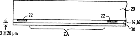
For example, the thickness of permanent substrate approximately is 500 microns, and diameter is 15-20 centimetres; The thickness of silicon chip was 500-1000 microns (diameter is 15-30 centimetres) in thinning in the past, and thinning is 3-20 microns later on.
The layer of the complanation that is formed by for example polyimides can be in the middle of silicon chip sends to before the substrate and be deposited on the silicon chip before sending permanent substrate to from middle substrate.
Must be noted that under some situation that middle substrate can use from a collection of being repeated during to another batch of being produced.
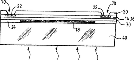
Therefore, the purpose of this invention is to provide a kind of imageing sensor, this imageing sensor comprises a transparent substrate, top at this substrate is superimposed with successively: the mosaic surface of colored filter, a very thin monocrystalline semiconductive layer that wherein is formed with the photosensitive area matrix (maximum ga(u)ge is tens microns) (30), an and stacked conductive layer and an insulating barrier, can make electric charge set the passing through transparent substrate that produces by the rayed photosensitive area, color filter layers, the photosensitive semiconductor district, arrive stacked conductive layer and insulating barrier then, thus can need not be before arriving the photosensitive area matrix through a conductive layer system.
Transparent substrate still also can be by pottery or crystalline material manufacturing preferably with glass or plastics manufacturing.
Description of drawings
Other advantage of the present invention and feature will be discussed in more detail below with reference to following accompanying drawing:
Fig. 1 is the structure that is formed on the imageing sensor on the silicon chip before the color filter layers location;
Fig. 2 is the operation that the front surface of silicon chip is sent to an interim substrate;
Fig. 3 is the interim substrate with the silicon chip after the thinning;
Fig. 4 is interim substrate, supports the silicon layer of thinning, deposits the mosaic surface of colored filter on this silicon layer;
Fig. 5 is permanent substrate, and wherein the surface with colored filter of interim substrate sends permanent substrate to;
Fig. 6 is a full depth permanent substrate afterwards of having removed interim substrate;
Fig. 7 is another optional embodiment, therein, only removes most of thickness rather than its full depth of interim substrate, and has wherein formed opening.
Embodiment
Shown in Figure 1 is the general structure of silicon chip, uses conventional art to form the image detection circuit of a plurality of imageing sensors thereon.
Image detection circuit (matrix of photosensitive point, transistor and interconnection line) is made on the surface of silicon chip, and this surface can be called as front surface, i.e. upper surface among Fig. 1.Described manufacturing comprises that at first the upper surface from silicon chip begins to carry out multiple diffusion and implant operation, to form very photosensitive area 12; Then, successively stacked conductive layer 14 and the insulating barrier 16 that is formed on 12 tops, photosensitive area deposited and etching operation; Described conductive layer and insulating barrier form the part of image detection circuit, and can make the set that produces electric charge by the image that projects on the transducer in the photosensitive area.
One of conductive layer 14 is one deck of last deposition substantially, is used for forming around the active region that comprises photosensitive dot matrix the I/O pad (pad is not shown at Fig. 1) of each independent transducer.
If make transducer with conventional art, the mosaic surface of colored filter can be deposited on the surface of silicon chip so.
According to the present invention, do not deposit colored filter in this stage, but on the front surface of silicon chip, adhere to an interim substrate 20 (Fig. 2).Interim substrate 20 is wafers that and silicon chip 10 have same diameter, and has the thickness close with it, to guarantee the rigidity of its structure during fabrication.And it also can be made of another silicon chip.Above-mentioned adhering to can carry out after the deposition plane layer, forms embossment (relief) feature by deposition and etching operation to stacked conductive layer and insulating barrier at the front surface of silicon chip.It is transparent that plane layer needs not to be.
Structure proportion shown in Figure 2 is littler than Fig. 1, is to comprise active region ZA and the whole separated sensor that is connected pad 22 around it in order to demonstrate.Pad 22 and conductive layer 14 contact or form the part of conductive layer 14, its preferably with silicon chip 10 and 20 between the interface flush; If deposited a plane layer, guarantee preferably that then plane layer does not cover pad 22.But if pad is covered by plane layer, the opening that can form at last in manufacture process leads to these pads so subsequently.
Silicon chip is sent to supporting wafers 20 can use several different methods.The simplest method can adhere to molecule and control silicon chip, because the surperficial plane degree (planeity) of these that are in contact with one another produces very large contact force (contact force).Also may adopt the method for gummed.
After the front surface with silicon chip was sent to supporting wafers, the major part of silicon wafer thickness was removed, and made only to stay about 8-30 microns thickness by the thickness that comprises lamination.The remainder of silicon chip is not more than the lamination 14,16 of several microns (such as 5-10 microns), and comprises that the remaining silicon wafer thickness of photosensitive area 12 is approximately 3-20 microns.Described remaining thickness is layer 30 the thickness of Fig. 3 that comprises the photosensitive area of Fig. 1.
The operation of thinning can adopt machining (grinding) back to finish up with chemical operation, perhaps mechanical/chemical processing method, perhaps only adopt the chemical machinery processing method, perhaps adopt a kind of specific process of separation again, be necessary to inject in advance in the plane impurity of embrittlement, the silicon layer of this plane and thinning is divided the boundary line.
Under the situation of separating, must before sending supporting wafers to, inject silicon chip by implanted dopant.In fact, implant operation is that the front surface at silicon chip carries out, and on the whole surface of wafer and arrive a degree of depth, this will limit cutting planes; Inject in advance and be preferably the hydrogen injection.It can carry out in any stage of making silicon chip, but can only carry out when silicon chip bonds to supporting wafers in the separation on the thickness at the wafer along the cutting planes that injects.
Can handle (fine lapping, chemical cleaning, mechanical/chemical polishing etc.) to the upper surface of the silicon wafer layer after the thinning 30 thus eliminate the defective on surface, the deposition etch colored filter forms common structure a plurality of sensor wafers as shown in Figure 2 then.
The mosaic surface 18 of colored filter is deposited on the surface of silicon wafer layer 30 (Fig. 4) then.If wish, one or more extra plays can be before the colored filter deposition deposition, particularly passivation layer, anti-reflection layer and other layer, for example, the electricity of doping silicon layer (electrode layer) activates necessary layer.
If necessary, the layer 24 of a complanation is deposited on the mosaic surface of colored filter.If it covers colored filter, then it must be transparent.The front surface with colored filter of interim then substrate 20 sends permanent transparent substrate 40 (by glass or plastics manufacturing) to, and this permanent substrate is a wafer that has same diameter with substrate temporarily and initial silicon chip.The thickness of permanent substrate equals the hundreds of micron at least, makes to guarantee that the rigidity of structure becomes possible (Fig. 5) in the manufacture process.
Interim substrate sends permanent substrate to and is to use gummed (employing transparent adhesive tape mixture) or molecule to adhere to carry out.
Under situation shown in Figure 6, substrate 20 is all removed, up to making the surface that connects pad 22 and described structure closely combine.
Under situation shown in Figure 7, substrate 20 is just partly removed.Stay very little thickness (if possible maximum several microns), wherein will use chemical etching or other method to form opening 70, to open near the zone that connects pad 22.
Connection pad under the situation of Fig. 7 can be used as with " wired joint (wire-bonding) " type of printed circuit board (PCB) and be connected.Because light must penetrate from permanent transparent substrate 40 sides, thereby printed circuit board (PCB) must be opened and makes it face the photaesthesia active region of transducer then.
Under situation shown in Figure 6, the upper surface that connects pad 22 and imageing sensor is combined closely.Their " wired joint " types that can be used to connect or " flip-chip (flip-chip) " type connects (this chip is reversed the corresponding pad of placement against printed circuit board (PCB) with connecting pad).In this case, transducer is illuminated by the top of printed circuit board (PCB).
If still want transducer shown in Figure 7 is used the assembly of flip chip type, wherein push opening 70 connecting pad 22, technology below will using: deposition and additional metal level of etching, this metal level are placed on the surface than the outside (promptly being formed with the upper surface of remainder of the substrate 20 of opening 70) of described structure and the bottom of opening 70.The outside of this structure connects the outside that pad will be formed at opening 70 then.
In these different embodiment, the structure that forms on substrate 40 can be tested on wafer with connecting pad.Described test can be carried out before light, image graphics etc.
Described structure is cut into independent transducer, is used for assembling at last in manufacture process.
Permanent substrate be attached to closely thinning with colored filter silicon layer on, its protection colored filter and silicon.
Claims (8)
1. method that is used for the shop drawings image-position sensor comprises:
Front surface at semiconductor chip (10) forms a series of active regions (ZA) that comprise the image detection circuit, and the corresponding corresponding imageing sensor in each active region; Each active region all by I/O pad (22) around,
Transmit semiconductor chip (10) and make the front surface of its front surface against interim supporting substrate (20),
On thickness, remove the major part of semiconductor chip, on substrate, stay the very carefully thin semiconductor layer (30) of one deck, this carefully thin semiconductor layer comprises the image detection circuit,
This method is characterized in that:
At first, colored filter (18) layer is deposited on the semiconductor layer, and is etched then, thus thinning,
Secondly, after the etching color filter layers, interim substrate is passed to transparent permanent substrate (40), this transparent permanent substrate (40) is applied to that side that interim substrate has colored filter,
Then, remove the major part of interim substrate (20) at least, so that be easy near I/O pad (22),
At last, substrate is cut into independent transducer.
2. the method for claim 1 is characterized in that, described interim substrate is all removed, and makes I/O pad (22) expose out.
3. the method for claim 1 is characterized in that, described interim substrate is partly removed, and stays next thin layer to protect semiconductor chip, forms opening (70) with near I/O pad (22) in this thin layer.
4. as each described method of claim 1 to 3, it is characterized in that semiconductor layer (30) has 3-20 microns thickness after thinning.
5. as each described method of claim 1 to 3, it is characterized in that described semiconductor chip (10) deposited a plane layer thereon before sending interim substrate to.
6. as each described method of claim 1 to 3, it is characterized in that the semiconductor layer of described thinning (30) deposits a transparent plane layer (24) on it before sending permanent substrate to from middle substrate.
7. imageing sensor, comprise a transparent substrate (40), be superimposed with the mosaic surface of colored filter (18) successively on the top of this transparent substrate (40), extremely thin single-crystal semiconductor layer (30), in this single-crystal semiconductor layer (30), be formed with the photosensitive area matrix, and stacked conductive layer (14) and insulating barrier (16), make through the set of transparent substrate by the irradiation generation electric charge of photosensitive area, thereby make light pass through transparent substrate successively, colored filter, the photosensitive semiconductor district, arrive stacked conductive layer and insulating barrier then, and need not be through a system that forms by a plurality of conductive layers before light arrives the photosensitive area matrix.
8. the described imageing sensor of claim 7 is characterized in that, transparent substrate (40) is to make with glass, plastics or crystalline material.
Applications Claiming Priority (2)
| Application Number | Priority Date | Filing Date | Title |
|---|---|---|---|
| FR0111335A FR2829290B1 (en) | 2001-08-31 | 2001-08-31 | COLOR IMAGE SENSOR ON TRANSPARENT SUBSTRATE AND MANUFACTURING METHOD |
| FR01/11335 | 2001-08-31 |
Publications (2)
| Publication Number | Publication Date |
|---|---|
| CN1550041A CN1550041A (en) | 2004-11-24 |
| CN100487899C true CN100487899C (en) | 2009-05-13 |
Family
ID=8866878
Family Applications (1)
| Application Number | Title | Priority Date | Filing Date |
|---|---|---|---|
| CNB028170423A Expired - Fee Related CN100487899C (en) | 2001-08-31 | 2002-08-30 | Colour image sensor on transparent substrate and method for making same |
Country Status (10)
| Country | Link |
|---|---|
| US (1) | US6933585B2 (en) |
| EP (1) | EP1421622B1 (en) |
| JP (1) | JP4147187B2 (en) |
| KR (1) | KR100919964B1 (en) |
| CN (1) | CN100487899C (en) |
| CA (1) | CA2457899C (en) |
| DE (1) | DE60223263T2 (en) |
| FR (1) | FR2829290B1 (en) |
| IL (2) | IL160113A0 (en) |
| WO (1) | WO2003019667A1 (en) |
Families Citing this family (11)
| Publication number | Priority date | Publication date | Assignee | Title |
|---|---|---|---|---|
| FR2863773B1 (en) * | 2003-12-12 | 2006-05-19 | Atmel Grenoble Sa | PROCESS FOR THE PRODUCTION OF AMINCI SILICON ELECTRONIC CHIPS |
| JP4486043B2 (en) * | 2004-12-30 | 2010-06-23 | 東部エレクトロニクス株式会社 | CMOS image sensor and manufacturing method thereof |
| KR100741920B1 (en) * | 2004-12-30 | 2007-07-24 | 동부일렉트로닉스 주식회사 | method for fabricating CMOS image sensor |
| US8791006B2 (en) | 2005-10-29 | 2014-07-29 | Stats Chippac, Ltd. | Semiconductor device and method of forming an inductor on polymer matrix composite substrate |
| US8409970B2 (en) * | 2005-10-29 | 2013-04-02 | Stats Chippac, Ltd. | Semiconductor device and method of making integrated passive devices |
| US8158510B2 (en) | 2009-11-19 | 2012-04-17 | Stats Chippac, Ltd. | Semiconductor device and method of forming IPD on molded substrate |
| DE102006014247B4 (en) * | 2006-03-28 | 2019-10-24 | Robert Bosch Gmbh | Image recording system and method for its production |
| US20090174018A1 (en) * | 2008-01-09 | 2009-07-09 | Micron Technology, Inc. | Construction methods for backside illuminated image sensors |
| JP5347520B2 (en) | 2009-01-20 | 2013-11-20 | ソニー株式会社 | Method for manufacturing solid-state imaging device |
| US8310021B2 (en) * | 2010-07-13 | 2012-11-13 | Honeywell International Inc. | Neutron detector with wafer-to-wafer bonding |
| EP3417476A1 (en) * | 2016-02-16 | 2018-12-26 | G-Ray Switzerland SA | Structures, systems and methods for electrical charge transport across bonded interfaces |
Family Cites Families (7)
| Publication number | Priority date | Publication date | Assignee | Title |
|---|---|---|---|---|
| US4758734A (en) * | 1984-03-13 | 1988-07-19 | Nec Corporation | High resolution image sensor array using amorphous photo-diodes |
| US4976802A (en) * | 1989-10-16 | 1990-12-11 | Xerox Corporation | Process for assembling smaller scanning or printing arrays together to form a longer array |
| JPH05183141A (en) * | 1991-07-12 | 1993-07-23 | Fuji Xerox Co Ltd | Color image sensor |
| US5244817A (en) * | 1992-08-03 | 1993-09-14 | Eastman Kodak Company | Method of making backside illuminated image sensors |
| US6059188A (en) * | 1993-10-25 | 2000-05-09 | Symbol Technologies | Packaged mirror including mirror travel stops |
| JPH0945886A (en) * | 1995-08-01 | 1997-02-14 | Sharp Corp | Amplifying semiconductor image pickup device |
| US6204087B1 (en) * | 1997-02-07 | 2001-03-20 | University Of Hawai'i | Fabrication of three-dimensional architecture for solid state radiation detectors |
-
2001
- 2001-08-31 FR FR0111335A patent/FR2829290B1/en not_active Expired - Fee Related
-
2002
- 2002-08-30 JP JP2003523013A patent/JP4147187B2/en not_active Expired - Fee Related
- 2002-08-30 IL IL16011302A patent/IL160113A0/en unknown
- 2002-08-30 DE DE60223263T patent/DE60223263T2/en not_active Expired - Lifetime
- 2002-08-30 CA CA2457899A patent/CA2457899C/en not_active Expired - Fee Related
- 2002-08-30 WO PCT/FR2002/002977 patent/WO2003019667A1/en active IP Right Grant
- 2002-08-30 US US10/485,694 patent/US6933585B2/en not_active Expired - Fee Related
- 2002-08-30 EP EP02796331A patent/EP1421622B1/en not_active Expired - Fee Related
- 2002-08-30 KR KR1020047001560A patent/KR100919964B1/en not_active IP Right Cessation
- 2002-08-30 CN CNB028170423A patent/CN100487899C/en not_active Expired - Fee Related
-
2004
- 2004-01-29 IL IL160113A patent/IL160113A/en not_active IP Right Cessation
Also Published As
| Publication number | Publication date |
|---|---|
| KR20040047783A (en) | 2004-06-05 |
| FR2829290B1 (en) | 2004-09-17 |
| KR100919964B1 (en) | 2009-10-01 |
| EP1421622A1 (en) | 2004-05-26 |
| US6933585B2 (en) | 2005-08-23 |
| EP1421622B1 (en) | 2007-10-31 |
| CA2457899A1 (en) | 2003-03-06 |
| IL160113A0 (en) | 2004-06-20 |
| JP2005501420A (en) | 2005-01-13 |
| CN1550041A (en) | 2004-11-24 |
| JP4147187B2 (en) | 2008-09-10 |
| IL160113A (en) | 2009-07-20 |
| DE60223263D1 (en) | 2007-12-13 |
| WO2003019667A1 (en) | 2003-03-06 |
| FR2829290A1 (en) | 2003-03-07 |
| CA2457899C (en) | 2012-07-03 |
| DE60223263T2 (en) | 2008-08-14 |
| US20040188792A1 (en) | 2004-09-30 |
Similar Documents
| Publication | Publication Date | Title |
|---|---|---|
| US7217590B2 (en) | Color image sensor with enhanced colorimetry and method for making same | |
| US5455455A (en) | Methods for producing packaged integrated circuit devices and packaged integrated circuit devices produced thereby | |
| US6117707A (en) | Methods of producing integrated circuit devices | |
| US20170170341A1 (en) | Integrated circuit device | |
| CN104009054B (en) | Semiconductor device, manufacturing method thereof, and electronic apparatus | |
| CN101419952B (en) | Wafer stage chip encapsulation method and encapsulation construction | |
| US7303400B2 (en) | Package of a semiconductor device with a flexible wiring substrate and method for the same | |
| KR100840502B1 (en) | Semiconductor device and manufacturing mathod thereof | |
| CN100487899C (en) | Colour image sensor on transparent substrate and method for making same | |
| US6960483B2 (en) | Method for making a color image sensor with recessed contact apertures prior to thinning | |
| US5552596A (en) | Three-dimensional radiation detection device and process for the production of said device having elementary reading circuits hybridized by welding microbeads | |
| US6972210B2 (en) | Method for making a color image sensor with pad-to-pad soldered supporting substrate | |
| CN105023931A (en) | Backside illuminated image chip module structure and fabrication method thereof | |
| CN106571377A (en) | Image sensor module and manufacturing method thereof | |
| CN101383300B (en) | Wafer level package of electronic element and manufacturing method thereof | |
| US20020086506A1 (en) | Method of fabricating an integrated circuit processed on both sides | |
| JP2001319996A (en) | Manufacturing method of semiconductor device |
Legal Events
| Date | Code | Title | Description |
|---|---|---|---|
| C06 | Publication | ||
| PB01 | Publication | ||
| C10 | Entry into substantive examination | ||
| SE01 | Entry into force of request for substantive examination | ||
| C14 | Grant of patent or utility model | ||
| GR01 | Patent grant | ||
| C17 | Cessation of patent right | ||
| CF01 | Termination of patent right due to non-payment of annual fee |
Granted publication date: 20090513 Termination date: 20120830 |