[0001] present patent application is incorporated into following patent application in the application's text in the mode of reference, comprise U.S. Provisional Application number 60/397,749 (submitting) on July 20th, 2002, U.S. Provisional Application number 60/435,400 (submitting) on December 20th, 2002, U.S. Provisional Application number 60/469,572 (submitting) on May 9th, 2003; Present patent application also is incorporated into following PCT patent application in the application's text in the mode of reference, comprise PCT application number PCT/US03/22537, exercise question is " Impedance Based Apparatuses andMethods for Analyzing Cells and Particles ", and the patent agent is numbered ACEA-0203.
Description of drawings
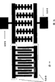
[0036] Figure 1A is the diagram of a device 100, and wherein two electrode structures with same or similar area are positioned on the substrate. first electrode structure has electrod assembly 110a, 110b, 110c; Second electrode structure has electrod assembly 120a, and the electrod assembly in the 120b, 120c and 120d. electrode structure is connected with each other by arcual connection electrode bus 125.The same with electrod assembly, connect bus (125) and also make (as gold thin film, platinum film, gold thin film is covered on chromium or the titanium film) by electro-conductive material.These conduction connecting paths or connection bus (125) can have an insulating coating.Electrod assembly 110a-110c and 120a-120d comprise electrode wires, and the circle of connection is arranged on this line.The total area in electrod assembly and electrod assembly gap may meet, and perhaps is a bit larger tham, or is slightly smaller than the end, hole (as: garden cylindrical hole, taper hole, cube hole), for example can use: 24,96, or 384 orifice plates.The all surfaces in hole can be covered by electrode, causes the variation of impedance to guarantee interaction of molecules on the lower surface of hole.Such arrangement has an advantage, promptly in the uneven interaction of molecules of hole basal surface generation, only can cause the little difference of the impedance of electrode structure 110 and 120 measurements.The 150th, the connection gasket .130 that can link to each other with the external impedance metering circuit be connection electrode structure 110 and 120 with the trace that is electrically connected of connection gasket.Described connection trace can extend with any direction on electrode plane.Figure 1B is the diagram of device 200, and two electrode structures that area is similar are arranged on its substrate.Electrode structure 210 and 220 comprises a plurality of interconnective electrod assemblies.Electrod assembly (210a-210c, 220a-220d) be the rectangle straight line, the common electrode structure unit of forming an alternating expression. be similar to Figure 1A, electrod assembly in each electrode structure (210a-210c 220a-220d) is connected with each other by arcual conductive path or electrode bus (225). and connection gasket 250 is connected on the electrode structure by being electrically connected trace 230.Fig. 1 C is the diagram of a device 300, and two electrode structures that area is similar are arranged on its substrate.Electrode structure 310 and 320 comprise a plurality of interconnective electrod assemblies (310a-310f, 320a-320f).(310a-310f 320a-320d) is rectangular lines to electrod assembly, forms a staggered electrode structure unit jointly, and different with Figure 1A and 1B, the electrode structure with electrod assembly 310a-310c and 320a-320c is connected on the connection gasket 350.
[0037] Fig. 2 illustrates the system of monitoring impedance variations, and impedance variations is because target molecule is caught in or is attached to electrode surface and causes." Y " symbolic representation in the diagram molecule of the seizure on the electrode surface. " Δ " symbolic representation in the diagram can be incorporated into the target molecule of catching on the molecule.Left figure has shown the background impedance (Z before the binding target molecule
0), right figure has shown the measurement impedance (Z after the seizure molecule binding target molecule
The molecule combination).With electric impedance analyzer or impedance detection circuit monitoring impedance.Those skilled in the art are very familiar to electric impedance analyzer.
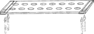
[0038] Fig. 3 illustrates 96 pore electrod plates that are used for Molecular Detection, on the substrate that is equipped with corresponding to the bottom surface, hole, assemble or inserted the detection microelectrode array. clear for the sake of simplicity, the structure that does not show hole wall among the figure. the electrode wires 450 that is positioned at Fig. 3 left side is the connection gaskets between microelectrode array and external impedance testing circuit. each hole (or at least some holes) all have two electrode structures, form an electrode structure unit, two connection gaskets are used in each hole like this, comprise the electrode structure that is used for device in the hole.In order to illustrate, shown the electrical connection of the electrode structure that is positioned at two upper left holes 460 and 470 on the figure.A kind of method that constitutes these class 96 pore electrod plates is that the substrate that will have electrode structure is attached to and has on the plate of managing array, the microtiter plate (as microtiter plate) that does not for example have the end, so that substrate forms the bottom of hole or fluid container, can be used for monitoring the interaction of molecule.
[0039] Fig. 4 A has illustrated a kind of device of measuring the molecule combined impedance, and this impedance is between unitary electrode and its adjacent electrode.As shown in the figure, circular electrode 410 has 6 adjacent circular electrodes 420.Can measure the impedance between discoid electrode 410 and all electrodes 420 (they interconnect) outside device. Fig. 4 B illustrates the device with a plurality of circular electrodes.
[0040] Fig. 5 has illustrated to have the electrode 510 of two different area and 520 device.
[0041] Fig. 6 has illustrated to have 9 unitary Molecular Detection plates of electrode structure, and all there are two electrodes each electrode structure unit. and an impedance measurement analyser can be changed between 9 unit and carry out impedance measurement.
[0042] Fig. 7 has illustrated electrode geometry, and these electrodes can be used for detecting or analyzing molecules in the present invention.7 (A), staggered, the parallel lines electrod-array, electrode width can greater than, be equal to or less than electrode gap; 7 (B) profile of tooth, the electrode structure of dislocation; 7 (C) add the electrode structure of disk electrode on electrode wires; 7 (D) profile of tooth, the straight electrode structure; 7 (E) sinusoidal electrode structure; 7 (F) coaxal electrode structure. the characteristic dimension of electrode can be as small as less than 10 microns, and is perhaps big extremely greater than the hundreds of micron.Total active electrode area can have different the shapes for example shape such as the rectangle (Fig. 7 (A), 7 (B), 7 (E)) of rule, or circular (Fig. 7 (C), 7 (D)), or Else Rule or irregular shape.Preferably, the electrode region total area (described area comprises electrode and interelectrode gap) has covered almost whole bottom surfaces of last chamber.Electrode structure is connected to impedance detection circuit (as electric impedance analyzer) through connection gasket and goes up (shown in Fig. 7 (A) and 7 (B)).Connection gasket can be directly connected on the electrod assembly (Fig. 7 (A), 7 (C) and 7 (E)) or be connected to (Fig. 7 (B) and 7 (D)) on the electrod assembly by additional electric connection structure.At Fig. 7 (A), (C) and (E) in, connection gasket also is that the conduction that is connected to the electrod assembly in the electrode structure connects trace.
[0043] Fig. 8 has illustrated the signal in the molecular detection to amplify, and it participates in by measuring the target small molecules, is realized by the product of the catalyzed reaction of enzyme mediation.As shown in the figure, the impedance variations that measures can illustrate the catalysate that the reaction that mediates from enzyme is arranged at sensor surface.In a kind of demonstration methods, the reaction of enzyme mediation occurs on the electrode surface, catalysate from solution precipitation on the surface of transmitter.Can monitor the existence and the quantity of catalytic reaction products on the electrode to the measurement of resistance.
[0044] Fig. 9 illustrative with device dynamic monitoring catalytic reaction products of the present invention precipitation.Device comprises a glass substrate (1cm
2Square), assemble a microelectrode structural unit above.The film that gold (about 0.2 micron) covers chromium (about 0.03 micron) is plated on the glass substrate. and customization and assembling have the microelectrode structural unit of " circle is on line " electrode geometry.For using appts, the cylindrical plastic hole of a hollow is connected on the microelectrode device, and therefore after sample joined in the plastic eyelet, the electrode structure unit was exposed in the experimental liquid hole.The microelectrode surface is to wrap quilt in advance with biotinylation bovine serum haemproteins (BSA), at room temperature seals 30 minutes with the solution that contains 3% milk powder again.After the simple cleaning of phosphate-buffered saline (PBS), (AP, 10ng/ml) incubated at room temperature is 30 minutes, fully cleans with PBS again to add the Streptavidin alkaline phosphatase.Alkaline phosphatase substrate BCIP/NBT (from S igma, BCIP:5-bromo-4-chloro-3-indyl phosphoric acid; NBT: four file nitroblues) join in the solution, the impedance in the plastic eyelet between electrode structure can detect with the Resistance Analysis instrument again.The reaction (the substrate B CIP/NBT of AP is transformed in the throw out) of AP mediation produces the precipitation (see figure 8) at the electrode structure cell surface.This precipitation causes the impedance between the electrode structure unit to increase. and As time goes on, more and more be deposited in electrode surface and produce, detect more and more higher impedance.By the time-dependent manner impedance between the potential electrode structural unit, can monitor the time-dependent manner AP activity of electrode surface.
[0045] Figure 10 shows that use device of the present invention comes the detection by quantitative fibronectin by impedance analysis.Device is similar to the sort of device that uses in Fig. 9.Device comprises a glass substrate (1cm
2Square), be equipped with a microelectrode structural unit above.The film that gold (about 0.2 micron) covers chromium (about 0.03 micron) is plated on the glass substrate.Customization and assembling have the microelectrode structural unit of " circle is on line " electrode geometry. and for using appts, the cylindrical plastic hole of a hollow is connected on the microelectrode device.Therefore after sample joined in the plastic eyelet, the electrode structure unit was exposed in the experimental liquid sample. and the fibronectin of different quantities (5ng, 500pg and 50pg) is added in the plastic eyelet, and at room temperature cultivates 2 hours.The step of this cultivation has caused on the pan coating of device one deck fibronectin molecule. and the surface of device was at room temperature sealed 1 hour with the solution that contains 3% milk powder again.After the simple cleaning of PBS, mouse-anti fibronectin (dilution in 1: 200) is added into 4 ℃ of following overnight incubation in the device. and the cultivation of spending the night causes the fibronectin of apparatus surface to combine with mouse-anti fibronectin molecule.After the cleaning, the anti-mouse IgG of alkaline phosphatase (AP) labelled goat is added into, and at room temperature cultivates 1 hour, fully cleans then.The anti-mouse IgG of AP labelled goat that causes of this cultivation of 1 hour combines with the mouse anti fibronectin of apparatus surface. and the substrate B CIP/NBT of alkaline phosphatase (from Sigma, BCIP:5-bromo-4-chloro-3-indyl phosphoric acid; NBT: four file nitroblues) be added in the solution, the impedance in the plastic eyelet between electrode structure can be measured with the Resistance Analysis instrument again.The reaction (the substrate B CIP/NBT of AP is transformed in the precipitation) of AP mediation produces the precipitation (see figure 8) at the electrode structure cell surface.This precipitation causes the increase of impedance between the electrode structure unit.As time goes on, more and more be deposited in electrode surface and produce, can detect more and more higher impedance.Shown the variation that adds substrate B impedance after CIP/NBT30 minute in the drawings.This device can detect few fibronectin to 50 piks (pg) of apparatus surface bag quilt as shown in the figure.
[0046] Figure 11 illustrates a kind of microelectrode band (or electrode band) that is used for Molecular Detection. be equipped with the microelectrode structural unit on this substrate band.Substrate material includes but not limited to, glass, plastic tab or film, pottery, polymeric film, the isolator on the semi-conductor (as the silicon-dioxide on the silicon), glass fibre (as be used for printed circuit board (PCB) those) or other insulating material.Diversified little assembling or micromechanics manufacture method can be used to assembling or produce on-chip electrode structure unit.On the surface of electrod-array, specific molecule is anchored or combination or absorption. and the molecule of grappling can be a for example chemical compound of nucleic acid, peptide, protein and other molecules.These molecules can be anchored with different physics or chemical process, in conjunction with or be adsorbed onto the surface. the physical method that is used to wrap quilt including, but not limited to passive absorption, rotary coating molecular solution and oven dry, with the molecular solution point sample to specified electrode structure unit etc.The method that chemical surface is modified is including, but not limited to the chemical reaction on molecule self-assembly and surface.These physics or chemical process can be used for the modified electrode surface, make it the grappling chemical molecular.A single band can have a plurality of electrode structures unit.The surface of different electrode structure can be modified or be wrapped by different anchoring molecule, and each microelectrode structural unit surface all uses the molecule of unique types to carry out finishing like this. and grappling, combination, absorption or the molecule that deposits on the electrode structure cell surface with other method can be used as the seizure molecule. and the target molecule in the sample solution can combine with the seizure molecule or react.After target molecule is attached to and catches on the molecule, the interstructural resistance of the microelectrode in the electrode structure unit will change, and this variation can be detected or monitor by electric impedance analyzer or impedance detection circuit.In some cases, target molecule is by enzyme (for example, alkaline phosphatase, the AP among Figure 11) mark.Marker enzyme can be used to a catalyzed reaction makes the substrate (for example, the BCIP among Figure 11) of enzyme change product into.Can monitor product by resistance between the microelectrode structure.For example, product can be insoluble, and is deposited in the microelectrode body structure surface.Under other some situations, target molecule is labeled some specific " mark " molecule. and these tagged molecule can participate in special chemical reaction, this chemical reaction will produce product, and these products are can be by the impedance detection of spaning electrode structure monitored or measure.For example, product can be insoluble, and is deposited in the electrode structure surface.This class product is can be by measurement of resistance detected or measure, to provide about the qualitative or quantitative information of target molecule in the sample solution.
[0047] shown the unitary device of a kind of 15X of comprising electrode structure among Figure 12 (A), on-chip electrode is with 2 rows, the form of 8 row is arranged. and the details of electrode structure does not show, only show unitary two electrical connections of each electrode structure (electrode trace), be used for the connection electrode structure to the connection gasket of two ends that are positioned at substrate.A hole is " sky " hole, and finger-hole does not connect activity sensor. and emptying aperture is used as control wells. and electrode structure can have for example Figure 1A of different geometrical shapies, 1B, 1C, 5,6,7A-7F is shown.
[0048] shown a kind of unitary device of 16X electrode structure that on substrate, is arranged with among Figure 12 (B).The details of electrode structure is not shown, and has only shown unitary two electrical connections of each electrode structure (electrode trace), is used for the connection gasket of connection electrode structure to two ends that are positioned at substrate.Electrode structure can have different geometrical shapies, as Figure 1A, and 1B, 1C, 5,6,7A-7F is shown.
[0049] shown a kind of unitary device of 16X electrode structure that on substrate, is arranged with among Figure 12 (C).There is an alternating expression electrod-array each electrode structure unit.
[0050] Figure 13 (A) has shown a kind of little pcb board, and it can be connected with the connection gasket of substrate edge, on this substrate just like the 16X electrode structure unit shown in Figure 12 (A).Pcb board has 16 rectangular conductors, and they are arranged with the spacing of the connection gasket shown in Figure 12 (A).
[0051] Figure 13 (B) has shown two pcb boards of assembling, makes it and has the unitary substrate of 16X electrode structure and be connected.
[0052] Figure 13 (C) has shown two pcb boards of assembling, makes it and has the unitary substrate of 16x electrode structure and be connected, and the POGO-pin that wherein has aciculiform links to each other with lead from following.
[0053] Figure 14 (A) has shown a kind of flexible circuit (flex circuit), can be used for being connected to the edge of sensor board. the two sides of flexible circuit has a plurality of rectangle electrical leads, the electrical lead of one side can be connected on the connection gasket in the device shown in Figure 12 (A), and electrical lead can be connected on the impedance detection circuit simultaneously. and the corresponding electrical lead in the two sides of flexible circuit is interconnective.
[0054] Figure 14 (B) has shown flexible circuit has been linked to each other with device shown in Figure 12 (A). the electrical lead of flexible circuit one side is connected on the connection gasket of device.
[0055] Figure 14 (C) shown with two flexible circuits with have the unitary substrate of 16X electrode structure and be connected, wherein have aciculiform POGO-pin and link to each other with lead from following.
[0056] Figure 14 (D) has shown the metal holder that a class is made of wire, can be used to the connection gasket of one side on the substrate is connected to the another side of substrate.
[0057] Figure 14 (E) has shown the cross-sectional view of a metal holder, and this clip is connected to the connection gasket of substrate edge the another side (that is: the bottom surface of substrate) of substrate.Same one side at substrate has electrode structure and connection gasket.Can link to each other with the metal holder of substrate bottom surface with (directly be connected or pass through electric switch) aciculiform POGO-pin syndeton that electric impedance analyzer is electrically connected, so, electric impedance analyzer just is connected with on-chip electrode structure.
[0058] Figure 14 (F) has shown the metal holder with the metal wire making of another type, can be used for the connection gasket of substrate one side is connected to the substrate another side. the extra bending of the metal clip of this type can make them be connected on the connection gasket at (for example, passing through a welding compound) printed circuit board edge.
[0059] Figure 14 (G) has shown the horizontal whip face figure of a metal holder, and this clip is connected to the connection gasket of substrate edge the another side (that is: the bottom surface of substrate) of substrate.This metal holder is connected on the printed circuit board, and electric impedance analyzer can link to each other with this printed circuit board (PCB) direct or indirect (for example, via electric switch).
[0060] Figure 15 (A) has shown a kind of bottom view of 96-orifice plate, and the bottom surface is assembled with 6 devices.Each device all has 16X electrode-structural unit, and at the device edge connection gasket is arranged.
[0061] Figure 15 (B) has shown a kind of bottom view of 96-orifice plate, and the bottom surface is assembled with 6 devices.Four intermediary devices all have 16X electrode-structural unit, and at the device edge connection gasket are arranged.Two lateral devices have 14X electrode-structural unit, and there is connection gasket at the device edge.
[0062] Figure 16 has shown a kind of POGO-pin contents structure, can hold a plurality of POGO-pins, and can link to each other with 96 orifice plates shown in the 15B with Figure 15 A.
[0063] Figure 17 has shown a kind of multiwalled electrode structure.
[0064] Figure 18 has shown a kind of device based on the electrode band that is used for analysis of molecules.
[0065] Figure 19 illustrates based on impedance detection, the principle of work of monitoring molecule association reaction.
[0066] Figure 19 (A, C, E and G) is the cross-sectional view of a device of the present invention, has shown two electrodes.The seizure molecule of " Y " symbolic representation is to be anchored, place, and imports, or is attached to electrode surface.Catching molecule can be any molecule, and it can interact with the measured or monitored target molecule in the sample solution.Catching molecule can be antibody, peptide, part, acceptor, albumen, nucleic acid, Nucleotide, oligonucleotide, or any can interaction or the bonded molecule with target molecule.What show among Figure 19 (A, C, E and G) is the method for detection background impedance Z o, just on the potential electrode or be coated with or be coated with or be modified with and catch the impedance that divides the period of the day from 11 p.m. to 1 a.m.
[0067] Figure 19 (B) is the cross-sectional view of a device of the present invention, has shown to have two electrodes of catching molecule.At the seizure molecule of electrode surface with " Y " symbolic representation, target molecule is with " ◆ " symbolic representation, and with catch molecule and combine. catch molecule and target molecule form an interaction of molecules to or molecule combine right, thereby target molecule can combine with the seizure molecule.Target molecule can be a molecule any and the seizure interaction of molecules.The target molecule that contains under a cloud is a molecules of interest measured or monitoring in target molecule in the sample solution or the sample solution. as catching molecule, target molecule can be an antibody, antigen, peptide, part, acceptor, albumen, nucleic acid, Nucleotide, oligomerization thuja acid, or any can combining or interactional molecule with the seizure molecule. shown in the figure B is the measurement of impedance Z m, measuring electrode with the seizure molecular modification of binding target molecule. figure (A) and (B) be a pair of, they have shown that interelectrode impedance changes into Zm from Zo, the situation (B) after combining corresponding to the situation (A) that is modified with the seizure molecule on the electrode and target molecule and seizure molecule.
[0068] Figure 19 (D) is the cross-sectional view of a device of the present invention, has shown to have two electrodes of catching molecule.Catch molecule with " Y " symbolic representation at electrode surface, target molecule is with " ◆ " symbolic representation, and with catch molecule and combine.Be different from Figure 19 (B), the target molecule here is labeled tagged molecule or marking particle, with " ● " symbolic representation.Catch molecule and target molecule form an interaction of molecules to or molecule combine right, thereby target molecule can combine with the seizure molecule.Tagged molecule or marking particle are molecule or particle, and they can increase the change (Z of impedance
ML-Z
O), in other words, can the amplification detection signal.Target molecule can be a molecule any and the seizure interaction of molecules.The target molecule that has under a cloud is a molecules of interest measured or monitoring in target molecule in the sample solution or the sample solution.As catching molecule, target molecule can be an antibody, antigen, peptide, part, acceptor, albumen, nucleic acid, Nucleotide, oligonucleotide, or any can with catch interaction of molecules or bonded molecule.What (D) show is the impedance Z of detecting electrode
ML, described electrode is caught molecular modification with the target molecule bonded, and the target molecule here is labeled tagged molecule or marking particle.Figure (C) and (D) be a pair of, they have shown that interelectrode impedance is from Z
oChange into Z
ML, corresponding to being modified with the situation (C) and the target molecule of catching molecule on the electrode and catching molecule bonded situation (D).Tagged molecule among Figure 19 (D) or marking particle are used to amplify or further increase the change (Z of impedance
ML-Z
o).A non-limited example of tagged molecule is some big organic molecule, and its can influence electrode surface after occurring on the electrode ion or electronics pass through, and will cause the big variation of the inter-electrode impedance measured.An example of marking particle can be nanometer or micron-sized electrical isolation particle, semiconductor grain, or even conductive particle. another example of marking particle is nanometer or micron-sized liposome, has signal to amplify molecule on their surface.Electrode surface appears influencing in this marking particle on electrode ion or electronics pass through, and will cause the big change of the impedance of electrode measurements.
[0069] Figure 19 (F) is the cross-sectional view of a device of the present invention, has shown to contain two electrodes of catching molecule, catches molecule on the surface of electrode with " Y " symbolic representation, and target molecule is with " ◆ " symbolic representation, and with catch molecule and combine.Be different from Figure 19 (B), the target molecule here is labeled tagged molecule or marking particle, does expression with " ● " symbol.Catch molecule and target molecule formed an interaction of molecules to or molecule combine right, thereby target molecule can combine with the seizure molecule.Tagged molecule or marking particle are molecule or particle, and they can increase the change (Z of impedance
ML-Z
O), in other words, can the amplification detection signal.Here, amplify by some reaction moleculars (R) in tagged molecule or particle and the solution by tagged molecule or signal that particle caused specific reaction realization takes place.The product (P) of reaction is deposited or is deposited in electrode surface, causes interelectrode impedance Z
MPTarget molecule be any can with the molecule of catching interaction of molecules. the target molecule that has under a cloud is a molecules of interest measured or monitoring in target molecule in the sample solution or the sample solution.As catching molecule, target molecule can be an antibody, antigen, polypeptide, part, acceptor, albumen, nucleic acid, Nucleotide, oligonucleotide, or any can with catch interaction of molecules bonded molecule. what Figure 19 (F) showed is the impedance Z of detecting electrode
Mp, described electrode is caught molecular modification with the target molecule bonded, and the target molecule here is labeled tagged molecule or marking particle.Figure (E) and (F) be a pair of, they have shown that interelectrode impedance is from Z
oChange into Z
Mp, corresponding to being modified with the situation (E) and the target molecule of catching molecule on the electrode and catching molecule bonded situation (F).Tagged molecule among Figure 19 (F) or marking particle are used to enlarge or further increase the change (Z of impedance
Mp-Z
o).Specific reaction realization takes place by some reaction (R) molecule in tagged molecule or particle and the solution in the amplification of tagged molecule or particulate signal among Figure 19 (F), the product (P) of reaction is deposited or is deposited in electrode surface, the electronics and/or the ion that will influence electrode surface pass through, this has caused a big impedance variations. and the situation that shows among Figure 19 (F) can be considered to the special case of Figure 19 (D).
[0070] Figure 19 (H) is the cross-sectional view of a device of the present invention, shown and contained two electrodes of catching molecule, catch molecule with " Y " symbolic representation on the surface of electrode, target molecule is with " ◆ " symbolic representation, and with catch molecule and combine. be different from Figure 19 (B), the target molecule here is labeled tagged molecule or marking particle, make marks with " ● " symbol. catch interaction of molecules of molecule and target molecule formation to or molecule combine right, thereby target molecule can combine with the seizure molecule. tagged molecule or marking particle are molecule or particle, and they can increase the change (Z of impedance
ML-Z
O), in other words, can the amplification detection signal.Here, tagged molecule is an enzyme, and it is that reaction by substrate molecule (S) in enzyme mediation or the catalytic solution obtains that the signal of tagged molecule amplifies.The reaction product (P) of enzyme mediation is deposited or is deposited in electrode surface, measures the impedance (Z of the electrode that causes
MEP). target molecule be any can with the molecule of catching interaction of molecules. the target molecule that has under a cloud is a molecules of interest measured or monitoring in target molecule in the sample solution or the sample solution.As catching molecule, target molecule can be an antibody, antigen, peptide, part, acceptor, albumen, nucleic acid, Nucleotide, oligonucleotide, or any can combining or interactional molecule with the seizure molecule. what figure (H) showed is the impedance Z of detecting electrode
MEP, described electrode is caught molecular modification with the target molecule bonded, and the target molecule here is labeled tagged molecule or marking particle.Figure (G) and (H) be a pair of, they have shown that interelectrode impedance is from Z
oChange into Z
MEP, corresponding to being modified with the situation (G) and the target molecule of catching molecule on the electrode and catching molecule bonded situation (H). and tagged molecule among Figure 19 (H) or marking particle are used to enlarge or further increase the change (Z of impedance
MEP-Z
o).Here, tagged molecule is an enzyme, it is by enzyme mediation or catalytic that signal amplifies, substrate molecule in the solution (S) reaction obtained. the product (P) of the reaction of enzyme mediation is deposited or is deposited in electrode surface, measures the impedance (Z of the electrode that causes
MEP).The product (P) of reaction is deposited or is deposited in electrode surface, and the electronics and/or the ion that will influence electrode surface pass through, and this will cause a big impedance to change. and the condition that shows among Figure 19 (H) can be considered to the special case of Figure 19 (F).Having described in Fig. 8 is some examples that based signal is amplified reaction with the enzyme.
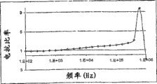
[0071] Figure 20 (A) has shown the typical frequency spectrum of the resistance that " circle on line " electrode structure of being assemblied on the glass substrate (live width=30 micron, line gap=80 micron, circular diameter=90 micron) records under different condition.The glass substrate that comprises electrode structure is formed electrode device. and plastic eyelet is assembled into and has constituted a test set on the electrode structure.The surface of electrode structure is fixed and goes up the alkaline phosphatase molecule, this is by at first wrapping on electrode by biotin labeled bovine serum albumin, then electrode is cultivated in the alkaline phosphate of Streptavidin, so that the alkaline phosphate (AP) that Streptavidin is modified combines with the vitamin H of electrode surface.At alkaline phosphate (AP) bag that Streptavidin is modified by after to electrode surface, wash fully with Tris (pH=7.6) damping fluid in the hole. and (17ul BCIP mother liquor is added among the 1.5ml Tris to comprise BCIP, the BCIP mother liquor is with the DMSO of 25mg/ml concentration preparation) and the Tris solution of NBT (33ul is added among the 1.5ml Tris, and the NBT mother liquor is prepared with the deionized water of 25mg/ml concentration) join in the hole. impedance measurement is carried out behind adding solution immediately or at thereafter different time.(a) symbol ◇ adds instant behind the solution, (b) symbol X,, ▲ corresponding after adding solution 13 (X), 28 () and 80 (▲) minute.
[0072] Figure 20 (B) shown with Figure 20 (A) the same terms under the measurement reactance frequency spectrum of same electrode structure: (a) symbol ◇, add instant behind the solution, (b) mark X,, ▲ respectively corresponding after adding solution 13 (X), 28 () and 80 (▲) minute.The reactance that shows in Figure 20 (B) is the absolute value of reactance, in other words, is meant the amplitude of reactance.The reactance that after adding solution, detects at once, 10Hz between the 500kHz be capacitive character and at 792kHz to being inductive character between the 5MHz. for other measurement, reactance is capacitive character between from 10Hz to 3.155MHz and is inductive character when 5MHz.
[0073] Figure 20 (C) has write down solution and has joined the ratio that the resistance of different time point measurement behind the hole and solution join the instant resistance value of measuring behind the hole.
[0074] Figure 20 (D) has write down solution and has joined the ratio that the reactance of different time point measurement behind the hole and solution join the instant reactance value of measuring behind the hole.
[0075] Figure 21 illustrates on the ACEA device specific detection and distinguishes that DNA Nucleotide replaces.This ACEA device has a glass substrate (about 18mm to 78mm), and 16 electrode structure unit are fitted thereon, and are arranged in the configuration of a 2X8, and the spacing of electrode unit is 9mm.The film that gold (about 0.2 micron) covers chromium (about 0.03 micron) is plated on the glass substrate. and the electrode structure unit has " circle is on line " electrode geometry (30 microns of live widths; Circular diameter: 90 microns, line gap: 80 microns), utilize thin film photolithography technology (photoresist deposition, the UV or the other light sources that cover through mask plate expose, the photoresist slaking, the photosensitive and corrosion film development, the wet corrosion gold, remove residual gold or other metals) molding and assembling. during using appts, one has 16 cylindrical circular holes in the no end, the plastic eyelet band of hollow is fixed on the electrode device, so the rear electrode structural unit is exposed in the laboratory sample solution in the plastic eyelet when sample joins.The diameter of sensor region is about 3mm, the diameter of plastic eyelet is about 6.5mm. before use, handled 15 minutes with 1N HCl on the surface of device, uses deionized water wash again. in order to test, synthesized three special oligonucleotide sequences (number of obtaining is D85722) of chlamydia trachomatis 16S ribosome-RNA(rRNA).They are that (a 1) length is 40 base pairs, the seizure oligonucleotide sequence (5 '-ZZZZGATTTGAGCGTACCAGGTAAAGAAGCACCG GCTAACTCCG) that 5 ' terminal sulfhydrylation is modified, (2) length are 20 base pairs, wild-type 5 ' terminal biotinylated target sequence (5 ' bio-CGGTGCTTCTTTACCTGGTA) and (3) length are 20 base pairs, 5 ' terminal biotinylated target sequence of sudden change, wherein single Nucleotide is substituted (C on No. 9 positions is substituted by A). in this experiment, catch oligonucleotide and be dissolved in the deionized water, concentration is 2 μ M.Tonya M.Herne and Michael J.Tarlov have reported a kind of more effective DNA method for coating (1M KH
2PO
4Compare H
2O is better) (Herne TM and Tarlov MJ, Characterization of DNA Probes Immobilized on Gold Surfaces.J.Am.Chem.Soc.1997,119,8916-8920). for the oligonucleotide sequence bag is arrived sensor surface, 100ul, the seizure oligonucleotide of 2 μ M is added in each transmitter, hatches under the room temperature 2 hours, cleans with PBS again.After the cleaning, sensor surface cleans with PBS with 0.3%BSA sealing 30 minutes again.For realizing DNA hybridization, in hybridization buffer (1.0M NaCl and 10mM Tris damping fluid, pH7.4 and 1mMEDTA), add 100 μ l, 1nM wild-type or 1nM mutant oligonucleotide sequence then join with the transmitter of catching oligonucleotide bag quilt.Negative control does not add target DNA.Hybridization was carried out 30 minutes at 42 ℃, clean with the phosphoric acid buffer that contains 50mMNaCl again. in order to detect DNA hybridization and to distinguish that mononucleotide replaces, the alkaline phosphatase of 100 μ l marked by streptavidin (1:2000 dilution in the Tris damping fluid) is added in each transmitter, and at room temperature hatched 30 minutes, use the Tris buffer solution for cleaning again. after the cleaning, 100 μ l alkaline phosphatase substrate mixtures, BCIP/BNT is added on the transmitter, real-time monitoring reaction on electric impedance analyzer.What as shown in the figure, the specific hybrid between seizure sequence and wildtype target sequence can be stabilized on electric installation detects.In the time of 60 minutes, the signal on the transmitter is higher 92.6 times than the signal that negative control transmitter produces. and the signal here is the resistance of measuring between the electrode structure in each hole under 5kHz.Compare mutant nucleotide sequence with the sequence of wild-type and only produce very faint signal with mononucleotide replacement.In the time of 60 minutes, the signal difference of wild-type sequence and mutant sequence is 30 times.
[0076] Figure 22 illustrates the system of monitoring impedance variations when cell attaches to electrode surface.
[0077] Figure 23 illustrates a kind of instrument, and its electrode face finish has the molecule that promotes that cell attaches.
[0078] Figure 24 is the diagram that cell migration detects, and the cell initial growth is at one, (not shown) on the growth district that is defined by removable orifice plate. being positioned at first on surveyed area or the surveyed area of the hole wall on the plate. and plate is removed subsequently.Cell is allowed to sprawl or moves to by coaxal electrode structure 2410 determined surveyed areas.
[0079] Figure 25 is the diagram that neurite outgrowth detects.Single neurone is positioned at the neurone anchor region at first.The variation of the impedance of 2510 on coaxal electrode structure can be used for monitoring neure growth in the surveyed area.
[0080] Figure 26 has shown 8 kinds of dissimilar electrodes resistance and reactance (mainly being condensive reactance) when being with or without the attaching of NI H3T3 cell.The unit of resistance and reactance all is Ohm.The amplitude of reactance all is drawn on the logarithmic plot.The polarity of reactance all is (condensive reactance) born under most of frequencies.In the result of Figure 32, different types of electrode is assembled in (1cm X 1cm X 1mm) on the glass substrate at Figure 26.Experimental installation all is not to be glued on the glass substrate that has electrode structure and to make by will there being the conical or columniform plastic pipe in the end. typically, at an end that glues mutually with glass substrate, the diameter of plastic pipe is 4.5mm to 6.2mm.Glass substrate has formed the end of hole (or fluid container), and plastic pipe forms the wall in hole (or fluid container).In the experiment, the cell of the suspension in substratum or substratum are added in the hole (or fluid container). and on-chip electrode structure is used to detect cell and attaches to caused impedance variations behind the electrode surface, comes the cell in the monitoring holes (or fluid container) to attach and/or growth with this.
[0081] Figure 27 electrode structure of illustrating use " 3B " shape comes the detection by quantitative cell.
[0082] Figure 28 electrode structure of illustrating use " 3C " and " 3B " shape is monitored the propagation of NIH3T3 cell and PAE cell in real time.
[0083] Figure 29 electrode structure of illustrating use " 3B " shape is monitored the NIH3T3 necrocytosis that UV-light (UV) causes in real time.
[0084] Figure 30 illustrates the IC of tamoxifen at different time toxic effect at interval
50Value.
[0085] Figure 31 electrode structure of illustrating use " 3C " shape comes the resistance value of four kinds of different cell types of comparison.
[0086] Figure 32 illustrates the repeatability of the measurement of impedance.
[0087] Figure 33 illustrates 5 kinds of representative design of the electric cell chip that is equipped with electrode structure on substrate.In the central zone of glass substrate, assembled the gold electrode (about 0.2 micron of thickness) that covers on the chromium coating (about 30 nanometers of thickness) with different shapes and size.The area of glass substrate is 1cm x 1cm.Electrode connection gasket on on-chip electrode structure is can be via glass-based unilateral links to each other with electro-detection interface (that is: impedance measuring circuit or electric impedance analyzer).
[0088] Figure 34 illustrates on test set four kinds of dissimilar cell detection or measurement. and these four kinds of cells are NIH 3T3 cell (inoblasts of mouse), PAE cell (aortic endothelial cell of pig), HUVEC (people's endotheliocyte), and pHuhep (people's primary hepatocyte).For NIH3T3 and pHuhep cell, electrode surface is with fibronectin bag quilt, and for PAE and HUVEC, electrode surface is with gelatin bag quilt.As shown in the figure, two devices are used for measuring each cell type. detected impedance at postvaccinal 0,3 and 4 hour. and during at 3 or 4 hours, NIH3T3 cell, HUVEC, PAE and pHuhep cell are all observed tangible resistance to be increased.To be used to obtain Figure 26 similar to the result's of Figure 32 test set, obtain the experimental installation of test-results shown in Figure 34 (with Figure 35 to Figure 37), be not to be glued on the glass substrate that has electrode structure and to make by will there being the conical or columniform plastic pipe in the end. glass substrate has formed the end, hole (or fluid container), the wall in plastic pipe formation hole (or fluid container).In the experiment, be added in the hole (or fluid container) at the suspension cell or the substratum of substratum.On-chip electrode structure is used to detect cell and attaches to caused impedance variations behind the electrode surface, comes the cell in the monitoring holes (or fluid container) to attach and/or growth with this.
[0089] Figure 35 illustrates the situation of monitoring PAE cell proliferation on test set in real time. and cell is inoculated on the electrode of bag tegillum with different concentration (8,000 cells and 1,000 cell).In order to monitor cell proliferation, resistance and reactance are detected on the different timed intervals. the mensuration immediately after " t0 " is shown as inoculating cell.Under two kinds of different cell inoculation density, resistance value all increases along with the increase of incubation time, illustrates that cell is in vegetative state.The high cell proliferation rate of inoculum density is apparently higher than the low cell of inoculum density.Sd: cell inoculation density.
[0090] Figure 36 has illustrated to carry out with test set and MTT analytical method pair cell the result of detection by quantitative.The NIH3T3 cell of serial dilution (10000,5000,2500,1250 and 625 cells) is added to bag by on the test set or 96 orifice plates of fibronectin.In the experiment of using appts, impedance is measurement in 16 hours behind inoculating cell.In MTT detected, cell was used MTT dyeing, reading under 540nm on the elisa plate reader again in back 16 hours in inoculation.As shown in the figure, device can detect the variation of cell number quantitatively.Two kinds of resulting results of detection method are very close.
[0091] Figure 37 illustrates the repeatability of measurement of resistance on the test set.Repeated experiment is to carry out on 6 devices of inoculating human primary hepatocyte.The resistance of each electrode is detected after 4 hours in (t0) and inoculation at once after the inoculation.Cultivate after 4 hours, all shown the increase of tangible resistance value on all devices, this indicates that cell is in the attaching of electrode surface (with other zones of substrate surface) with sprawl.Right figure has shown that the CV of t0 is 4.3%, and the CV of t4h is 2.7%.
[0092] Figure 38 (A) is presented under two kinds of different conditions, is assemblied in the typical frequency spectrum of " circle on line " the measured resistance of electrode structure on the glass substrate.(a) open symbols, the tissue culture medium (TCM) that contains the HT1080 cell are added in the hole that contains electrode structure in the near future the result that (in 10 minutes, cell is not adhesive electrode and substrate surface as yet) measured; (b) filled symbols, the substratum that contains the HT1080 cell joins the bottom surface, hole and includes the hole of electrode structure after 2 hours 40 minutes (cell has attached to electrode and substrate surface). and in 2 hours 40 minutes time, the hole is placed on 37 ° of C and contains 5%CO
2Incubator for tissue culture in.Live width is 30 microns in the electrode structure of 3B design, and line is spaced apart that successive circle diameter is 90 microns on 80 microns and the line.In this example, the total area (zone) that all electrodes and electrode gap cover is equivalent to the circle of one 3 mm dia.Electrode structure on the glass substrate has constituted the end of round taper hole, and the top end diameter in hole is approximately 6.5 millimeters and the diameter of bottom is about 5 millimeters.In experiment, contain about 7000 HT1080 cells, the tissue culture medium (TCM) of cumulative volume 100 microlitres has in the hole of electrode structure at the bottom of being added into the hole.
[0093] Figure 38 (B) be depicted as with Figure 38 (A) the same terms under, at the measured reactance frequency spectrum of identical electrodes. the absolute value of noting reactance is plotted as logarithmic value (similar with curve shown in Figure 26). and except the high frequency of 1MHz and 580kHz, the reactance that is added in the hole electrode structure that (in 10 minutes) in the near future record at the tissue culture medium (TCM) that contains the HT1080 cell all is a negative value (capacity reactance).Adding the reactance that the Kong Zhonghou contain electrode structure records in the time of 2 hours 40 minutes at cell suspending liquid, all is negative value at the whole range of frequency 100Hz that measures in 1MHz.
[0094] Figure 38 (C) has shown based on result shown in Figure 38 (A), the ratio frequency spectrum of the resistance value when having cell to be attached at electrode surface when resistance value and acellular attach.
[0095] Figure 38 (D) has shown based on result shown in Figure 38 (B), the ratio frequency spectrum of the reactance value when having cell to be attached at electrode surface when reactance value and acellular attach.Attention is when calculating the reactance ratio, and reactance polarity (electric capacity and inductive reactance) is taken into account.
[0096] Figure 39 (A) is presented under two kinds of different conditions, is assemblied in the typical frequency spectrum of " circle on line " the measured resistance of electrode structure on the glass substrate.(a) open symbols, the tissue culture medium (TCM) that contains the HT1080 cell are added in the hole that contains electrode structure in the near future the result that (in 10 minutes, cell is not adhesive electrode and substrate surface as yet) measured; (b) filled symbols, the substratum that contains the HT1080 cell joins the bottom surface, hole and includes the hole of electrode structure after 2 hours 40 minutes (cell has attached to electrode and substrate surface).In 2 hours 40 minutes time, the hole is placed on 37 ° of C and contains 5%CO
2Incubator for tissue culture in.Live width is 30 microns in the electrode structure of 3B design, line is spaced apart that successive circle diameter is 90 microns on 80 microns and the line. in this example, the total area (zone) that all electrodes and electrode gap cover is equivalent to the circle of one 3 mm dia. and the electrode structure on the glass substrate has constituted the end of round taper hole, the top end diameter in hole is approximately 6.5 millimeters and the diameter of bottom is about 5 millimeters. in experiment, contain about 3200 HT1080 cells, the tissue culture medium (TCM) of cumulative volume 100 microlitres has in the hole of electrode structure at the bottom of being added into the hole.
[0097] Figure 39 (B) be depicted as with Figure 39 (A) the same terms under, at the measured reactance frequency spectrum of identical electrodes. the absolute value of noting reactance is plotted as logarithmic value (similar with curve shown in Figure 26).High frequency except 1MHz and 580kHz, the reactance that is added in the hole electrode structure that (in 10 minutes) in the near future record at the tissue culture medium (TCM) that contains the HT1080 cell all is a negative value (capacity reactance). adding the reactance that the Kong Zhonghou that contains electrode structure records in the time of 2 hours 40 minutes at cell suspending liquid, all is negative value at the whole range of frequency 100Hz that measures in 1MHz.
[0098] Figure 39 (C) has shown based on result shown in Figure 39 (A), the ratio frequency spectrum of the resistance value when having cell to be attached at electrode surface when resistance value and acellular attach.
[0099] Figure 39 (D) has shown based on result shown in Figure 39 (B), the ratio frequency spectrum of the reactance value when having cell to be attached at electrode surface when reactance value and acellular attach. notice that reactance polarity (electric capacity and inductive reactance) is taken into account when calculating the reactance ratio.
[00100] Figure 40 (A) is presented under two kinds of different conditions, be assemblied in the typical frequency spectrum of " circle is on line " the measured resistance of electrode structure on the glass substrate. (a) open symbols, the tissue culture medium (TCM) that contains the HT1080 cell is added in the hole that contains electrode structure in the near future the result that (in 10 minutes, cell is not adhesive electrode and substrate surface as yet) measured; (b) filled symbols, the substratum that contains the HT1080 cell joins the bottom surface, hole and includes the hole of electrode structure after 2 hours 40 minutes (cell has attached to electrode and substrate surface). and in 2 hours 40 minutes time, the hole is placed on 37 ° of C and contains 5%CO
2Incubator for tissue culture in.Live width is 30 microns in the electrode structure of 3B design, and line is spaced apart that successive circle diameter is 90 microns on 80 microns and the line. in this example, the total area (zone) that all electrodes and electrode gap cover is equivalent to the circle of one 3 mm dia.Electrode structure on the glass substrate has constituted the end of round taper hole, the top end diameter in hole is approximately 6.5 millimeters and the diameter of bottom is about 5 millimeters. in experiment, contain about 500 HT1080 cells, the tissue culture medium (TCM) of cumulative volume 100 microlitres has in the hole of electrode structure at the bottom of being added into the hole.
[00101] Figure 40 (B) be depicted as with Figure 40 (A) the same terms under, at the measured reactance frequency spectrum of identical electrodes.The absolute value of noting reactance is plotted as logarithmic value (similar with curve shown in Figure 26). and except the high frequency of 1MHz and 580kHz, the reactance that is added in the hole electrode structure that (in 10 minutes) in the near future record at the tissue culture medium (TCM) that contains the HT1080 cell all is a negative value (capacity reactance).Adding the reactance that the Kong Zhonghou contain electrode structure records in the time of 2 hours 40 minutes at cell suspending liquid, all is negative value at the whole range of frequency 100Hz that measures in 1MHz.
[00102] Figure 40 (C) has shown based on result shown in Figure 40 (A), the ratio frequency spectrum of the resistance value when having cell to be attached at electrode surface when resistance value and acellular attach.
[00103] Figure 40 (D) has shown based on result shown in Figure 40 (B), the ratio frequency spectrum of the reactance value when having cell to be attached at electrode surface when reactance value and acellular attach.Attention is when calculating the reactance ratio, and reactance polarity (electric capacity and inductive reactance) is taken into account.
[00104] Figure 41 (A) has shown that the cell when different numbers joins the Kong Zhonghou that includes same type " circle on line " electrode structure (electrode shape 3B), the frequency spectrum of resistance ratios.Figure 41 (A) is Figure 38 (C), the summary of frequency spectrum shown in 39 (C) and 40 (C).The method of a kind of calculating " cell number index " is based on the frequency spectrum of these resistance ratios, at first determines the maximum value of resistance ratios, then maximum value is subtracted " one ".The cell number index that calculates by this method is adding different cell quantities 7000,3200 and had been respectively 5.17,1.82 and 0.17 at 500 o'clock.Obviously, cell quantity is big more, and the cell number index is high more.
[00105] Figure 41 (B) has shown that the cell of different numbers joins the Kong Zhonghou of " circle on line " electrode (electrode shape Fig. 3 B) that includes same type, the frequency spectrum of reactance ratio.Figure 41 (A) is Figure 38 (D), the summary of frequency spectrum shown in 39 (D) and 40 (D).
[00106] Figure 42 (A) has compared the alternating expression electrode structure of four kinds of different geometries, attach to resistance and the reactance frequency spectrum of electrode surface being with or without cell to measuring, these electrode structures have different electrode width counter electrode gap ratios. the resistance of the electrode structure when cell does not attach and reactance frequency spectrum, be to join (in 10 minutes, cell does not attach to electrode and substrate surface) that the back short period of time records in the culture hole that contains electrode at the tissue culture medium (TCM) that contains the 3T3 cell.Impedance when cell does not attach on the electrode structure and reactance frequency spectrum are to join in the culture hole that contains electrode at the tissue culture medium (TCM) that contains the 3T3 cell to record in back 3 hours.In this process of 3 hours, cell is placed on and is set to 37 ° of C, 5%CO
2In the incubator for tissue culture of level.Geometrical shape is 2AD, and the electrode structure of 2BE and 2CF is assembled on the glass substrate of 1cm X 1cm, and their electrode width is respectively 50,48 and 48 microns, and electrode gap is respectively 10,18 and 28 microns.The covering geometrical shape is 2AD, the zone in 2BE and 2CF electrode and gap thereof be equivalent to 1mm, the circle of 3mm and 6mm diameter respectively.The electrode width of the 4th kind of electrode structure and gap all are 50 microns and are assembled on Kapton (polyimide) substrate that the zone in coated electrode and gap is the rectangle of 6mm X 5mm.In these experiments, the bottom surface diameter be 4.5mm the conical plastic hole, be adhered to and have different alternating expression electrodes, on glass substrate or Kapton (polyimide) substrate. for the electrode structure of 2AD and 2BE geometrical shape, electrode structure is positioned on the central zone of bottom, hole.For the electrode structure and the Kapton substrate of 2CF geometrical shape, the bottom, hole is covered by electrode and electrode gap.Before the experiment, fibronectin is thoroughly cleaned and be coated with in the surface of electrode and substrate all. obviously, in the hole, add the 3T3 cell (about 10 of equal amts
4Individual cell), almost constant for width is 50 microns electrode, reduces the gap length between adjacent electrode, will cause cell to attach the back with respect to there not being cell to be attached to the increase of the impedance variations amplitude on the electrode.
[00107] Figure 42 (B) has shown the relation between the cell number index with different electrode widths and different staggered electrode of electrode gap ratio. it is to deduct 1 by maximum resistance ratio (ratio between resistance of measuring when having cell to attach to electrode surface and the resistance measured when not having cell to attach to electrode surface) to get under respective frequencies that the cell number exponential calculates.Obviously, be 50 microns width and add the 3T3 cell (about 10 of the equal amts in the hand-hole when almost constant for width
4Individual cell), the gap length that reduces between adjacent electrode will cause the cell number exponential to increase.From data as can be seen, when the ratio in width/gap is 1.5 or when bigger, cell number index (CI) has tangible increase.
[00108] Figure 43 illustrates two electrode sensings based on microfluidic channel.
[00109] Figure 44 illustrates the multi-electrode sensing based on microfluidic channel.Electrode 1 (1 ' link to each other with 1) and 4 (4 ' link to each other with 4) is used to provide one to flow through passage constant electric current, and electrode 2 (2 ' link to each other with 2) and 3 (3 ' link to each other with 3) is used to monitoring voltage.When cell by electrode 2 (2 ') and 3 (3 ') define regional the time, impedance is changed, this will cause electrode 2 (2 ') and the change of voltage between 3 (3 ').
[00110] Figure 45 illustrates when individual particle passes through on-chip micropore, and this particle is carried out impedance analysis.Here electrode be integrated in on-chip.
[00111] Figure 46 illustrates and detects impedance variations (Z simultaneously
1) attach and adhere on the electrode with the monitoring cell, and in the solution variation of specific conductivity (by Z
2The impedance variations reflection that detects).
About detailed description of the present invention
[00112] for clearly description, rather than for affected certain restriction, details of the present invention will be divided into a plurality of chapters and sections in following description.
A. definition
[00113] for clearly description, rather than for affected certain restriction, details of the present invention is divided into a plurality of chapters and sections in following description.
[00114] unless other definition is arranged, as used herein technology and science vocabulary all with the technical field of the invention in vocabulary have identical implication.All referred in this patents, patent application, disclosed application, and other publications all are incorporated in the text of the present invention by the form with reference.If definition of in this chapter, being set forth and the patent that is incorporated into the form of reference in the text of the present invention, patent application, disclosed application, and contradiction or inconsistent appears in the definition that other publications are set forth, and is as the criterion with the definition that this chapter was set forth so.
[00115] as used herein " one " refers to " at least one " or " one or more ".
[00116] as used herein " film " is meant material sheet.
[00117] as used herein " biocompatible membrane " refers to comprise viability by pair cell, attaches, and sprawls motion, growth, the harmless films of function such as division.
[00118] alive when containing, unimpaired, the suspension of epithelial cell or endotheliocyte is added in the vessel, the surface of vessel " being suitable for cell attaches " is meant that the cell adhesion that remarkable per-cent was arranged in 12 hours is in vessel surface. preferably, at least 50% cell adhesion is in vessel surface in 12 hours. more preferably, one be suitable for surface properties that surface that cell attaches has make bed board in (promptly after cell adds vessel) 12 hours at least 70% cell adhesion in the surface. even more preferably, the character that is suitable for the surface that cell attaches make at least 90% cell in the hole, shop adhesive surface in 12 hours.Most preferably, the character that is suitable for the surface that cell attaches make at least 90% cell in the hole, shop adhesive surface in 8,6,4,2 hours.Attach required surface properties in order to reach cell, the surface must be through chemical treatment (as: with acid and/or alkaline purification) and/or physical treatment (as: using plasma treatment), and/or biological treatment (as: help molecule or the biomolecules bag quilt that cell attaches with one or more. in this invention, a biocompatible surface (for example film), preferably, be the suitable employed cell type attaching in the detection of adopting biocompatible surface (for example film) that allows. guarantee most preferably that in detection 90% cell that contacts with biocompatible surface can attach thereon.
[00119] " biomolecules bag quilt " is meant the molecule bag quilt on the surface, and these molecules comprise natural biological molecule or biochemical molecule, or are derived and next molecule by natural biological molecule or biochemical molecule.For example, the biomolecules bag can be comprised extracellular matrix composition (as fibronectin, collagen), and or derivatives thereof also can comprise biochemical molecular, and as polylysine or poly ornithine, they are poly molecules of natural biological chemical molecular Methionin and ornithine.Based on natural biochemical molecular such as amino acid whose poly molecule, can utilize the isomer and the enantiomer of natural biochemical molecular.
[00120] " the outer cell substrate composition of born of the same parents " is meant the molecule that is present in the zooblast epimatrix.It can be the extracellular matrix components that derives from any species and any types of organization.The composition of extracellular matrix is including, but not limited to ln, collagen, and fibronectin, other glycoprotein, peptide, glycosaminoglycan, albumen is poly-sticking etc. and extracellular matrix components can also comprise somatomedin.
[00121] " electrode " is meant a kind of structure of high conductivity, the projecting far away material of its specific conductivity.
[00122] " electrode structure " at this indication is meant single electrode, particularly electrode (as the electrode structure of a spiral type), or the combination of the electrod assembly of at least two electric connections with complex construction. all parts in one " electrode structure " all are electric connections.
[00123] be meant single structure in the electrode structure at " electrod assembly " of this indication, for example, the digitation structure in the staggered electrode structure.
[00124] is meant that in " the electrode structure unit " of this indication two or more electrode structure forms the structure with certain size and interval, when being connected in signal source, can be used as the zone of a unit around electrode structure and produce electric field. preferred electrode structure unit can be measured because cell is attached to the impedance variations that electrode surface causes among the present invention.The electrode structure unit includes, but are not limited to staggered electrode structural unit and coaxal electrode structural unit.
[00125] " electrode trace " (electrode traces) is meant a conductive path that leads to device or instrument tip or border by electrode or electrod assembly or electrode structure, and with electrode, electrod assembly or electrode structure and electric impedance analyzer couple together.The end of device or border can be corresponding to the connection gaskets on device or the instrument.
[00126] " connection gasket " is a zone on device of the present invention or the instrument, it is electrically connected to instrument or device is gone up at least one electrode structure interior at least one electrode or all electrod assemblies, and can be connected to (as impedance detection circuit or signal source) on the circuit external in use.Electrical connection between connection gasket and impedance detection circuit or the signal source can be direct or indirect, can for example lead or metal wire are realized by any suitable conductive tool.This conductive tool also can realize through other regional electrodes or conductivity path on device or the instrument.
[00127] " interlock " raised structures that is meant a direction and from the raised structures of another direction with a kind of mode of the finger-shaped that overlaps stagger mutually (preferably can not be in contact with one another between the staggered like this electrod assembly).
[00128] referred in this " possibility of contacts electrode parts is big " be meant when cell by at random be put into instrument of the present invention or device during sensor region, the possibility of cell (or particle) contacts electrode parts is (by on device of the present invention or instrument or the mean diameter of the cell of interior use, the size of electrod assembly, the gap length of electrod assembly calculates) should be greater than about 50%, should be under the preferred situation greater than about 60%, should be under the preferred situation greater than about 70%, even more preferably greater than about 80%, about 90%, or about 95%.
[00129] " at least two electrodes that assemble on described substrate " are meant that at least two electrodes are assembled or make or produce on substrate. these at least two electrodes can be in the same one side of substrate or the not coplanar of substrate.Substrate can have multilayer, and these at least two electrodes can be in the same one deck of substrate or the different layers of substrate.
[00130] " at least two electrodes of assembling on described substrate one side together " are meant that at least two electrodes are assembled on the same one side of substrate.
[00131] " at least two electrodes that assemble on the same aspect of described substrate " are meant, if insulating substrate is a multiwalled, have at least two electrodes to be assemblied on same one deck of substrate so.
[00132] " described ... that electrode has essentially identical surface-area " is meant that the surface-area of the electrode of being mentioned does not have very big difference, thereby cell will occupy in overall detectable impedance variations in the impedance variations that attaches on another electrode or growth causes with cell in the impedance variations that attaches on described any one electrode or growth causes and have same or similar component.In other words, when electrode had essentially identical surface-area, the cell on arbitrary electrode attached or growth all can cause overall impedance variations.In general, electrode that " to have essentially identical surface-area " maximum and minimum interelectrode surface-area ratio are less than 10.Preferably, maximum electrode and minimum interelectrode surface-area ratio be less than 5,4, and 3,2,1.5,1.2 or 1.1.More preferably, at least two of described electrode structure electrodes have and are bordering on the area that is equal to or is equal to.
[00133] " described device have suitable cell attaches or the surface of growth " is that the zone of finger device top electrode and/or non-electrode has suitable physics, chemistry or biological nature, so that interested cell can be attached on this surface with surviving, and behind growth of cell culture, new cell can continue to be attached on the surface of device.Yet, comprise cells survival or grow not necessarily condition of necessary material at device or its surface.The material that these are necessary, for example nutrition or somatomedin can be by providing in the substratum.Preferably, intac when what live, epithelial cell or endotheliocyte suspension join " surface that suitable cell attaches " when going up, and have 50% cell adhesion in 12 hours at least to the surface.More preferably, the surface that a kind of suitable cell attaches has surface properties, so that bed board has 70% cell adhesion at least to the surface in (promptly adding cell to chamber that contains described device or hole) 12 hours. more preferably, the surface properties that suitable cell attaches will cause bed board to have 90% cell adhesion in 12 hours at least to the surface.Most preferably, the surface properties that attaches of suitable cell will make to have at least in behind bed board 8,6,4,2 hours of 90% cell and adhere on the surface.
[00134] " described interelectrode measurable impedance variations " be meant when the molecule association reaction when electrode surface takes place, will cause between electrode producing enough big impedance variations, this impedance variations can be recorded by electric impedance analyzer or impedance measuring circuit.Difference when impedance variations refers to the molecule association reaction be arranged and do not have the molecule association reaction on the electrode surface of device between the resistance value.Perhaps, impedance variations refer to as cell when electrode surface attaches impedance and the difference between the acellular resistance value when electrode surface attaches, or the variation of the cell number, kind, activity or the form that on attaching to device, contain the surface of electrode impedance when changing.In general, the impedance change promptly is measurable above 0.1%. preferably, measurable change in impedance value surpasses 1%, 2%, 5%, 8%.More preferably, measurable change in impedance value surpasses 10%.The function of the electric field frequency that interelectrode impedance is normally applied." the measurable impedance variations between the described electrode " also do not require that in all frequencies detectable impedance variations is arranged, and variation that need only impedance can be recorded one (or a plurality of frequency).In addition, impedance has two compositions, i.e. resistance and reactance (reactance can be divided into two classes, i.e. condensive reactance and inductive character reactance)." described interelectrode measurable impedance variations " is only required in that one of resistance and reactance have measurable variation under any one or a plurality of frequency.In this application, impedance is electricity or electronic impedance. the method that detects this impedance is, (1) between described electrode, provides a kind of CF (or multi-frequency, or have a special voltage waveform) voltage, and measure at CF (or multi-frequency, or have a special voltage waveform) down by the electric current of above-mentioned electrode, the voltage amplitude amplitude is obtained resistance value divided by the current amplitude value; (2) provide a kind of monofrequency composition electric current (or multi-frequency, or have a special waveform) by above-mentioned electrode, measure under CF (or multi-frequency, or have special waveform), voltage between the above-mentioned electrode obtains resistance value with the voltage amplitude amplitude divided by the current amplitude value; (3) can detect or measure other method of electric impedance.Note, above-mentioned " the voltage amplitude amplitude is obtained impedance divided by the current amplitude value ", " divided by " serve as current amplitude value and voltage amplitude amplitude under the identical frequency.Measuring this electric impedance is a kind of electronics or electric process, and it need not use any reagent.
[00135] " described at least two electrodes have visibly different surface-area " is meant that the surface-area of any electrode all is dissimilar each other, thus, the impedance variations that cell attaches or growth causes on large electrode, with the impedance variations that cell on small electrode attaches or growth causes, the component that is occupied in the detectable on the whole impedance variations is different or dissimilar.Preferably, can be significantly less than the impedance variations that cell attaches or growth causes on the small electrode in any impedance variations that cell on the large electrode attaches or growth causes.In general, the ratio of the area of extreme electrode and minimum electrode is greater than 10. preferably, and the ratio of the area of extreme electrode and minimum electrode surpasses 20,30,40,50 or 100.
[00136] " many counter electrode or electrode structure carry out spatial disposition according to the hole on the porous microtiter plate " is many counter electrode or the electrode structure on finger device or the instrument, the sterie configuration in the hole on the coupling porous microtiter plate is carried out spatial disposition, thus, device can be inserted into when needed, be attached to, or be attached to porous plate (for example, the porous plate at a no end), and a plurality of holes in the microtiter plate will comprise electrode or electrode structure.
[00137] " arrange " and be meant by the ranks configuration, just electrical connection, the position of electrode, but the circuit position of the position of electrod-array or a switch is number determined by a line position number and column position.
[00138] " each hole all comprises basic identical number ... cell " be that the minimum value of cell number is at least half of cell number maximum in the hole in the finger-hole.Preferably, the minimum value of number is at least 60%, 70%, 80%, 90%, 95% or 99% of cell number maximum in the hole.More preferably, every hole all comprises identical cell count.
[00139] " each hole all comprises the cell of same kind " be meant that with regard to specific purpose, every hole comprises the cell of same kind, but unnecessary every hole comprises complete same kind cell.For example, if being every hole, specific purpose comprises mammalian cell, so, each hole can comprise the mammalian cell of identical type, as human cell or different mammalian cell such as human cells, reach for example mouse of other inhuman mammalian cell, goat or MC etc.
[00140] " every hole comprises ... the test compounds of a series of different concns " be meant that the concentration of the test compounds that every hole comprises is serial dilution, be 1M as the concentration of 10/a series of dilutions, 0.1M, 0.01M etc.
[00141] " dose response curve " is meant the dependence of cell response to the test compounds dose concentration.The reaction of cell can detect by many different parameters. for example, test compounds is under a cloud to have cytotoxicity, can cause necrocytosis, so, the reaction of cell after test compounds is handled can record by the cell percentage of do not survive (or survival).
[00142] " electrode is more much smaller than the maximum one dimension size of the particulate of being analyzed along the length that major axis had of microchannel " is meant electrode in the length on the long axis direction of microchannel, is less than 90% of the maximum one dimension size of institute's analysing particulates.Preferably, electrode be less than in the length on the long axis direction of microchannel institute's analysing particulates maximum one dimension size 80%, 70%, 60%, 50%, 40%, 30%, 20%, 10%, 5%.
[00143] " microelectrode is striden the whole height of microchannel " be meant microelectrode stride at least the microchannel whole height 70%.Preferably, microelectrode is striden 80%, 90%, 95%. being more preferably of whole height of microchannel at least, microelectrode stride at least the microchannel whole height 100%.
[00144] " hole has the aperture that is equivalent to or is a bit larger tham described granular size " is meant that the aperture in this hole equals the particulate size at least, and this aperture is less than 300% of granular size.Here the measurement of aperture and particulate size dimension only limits to one dimensional numerical.
[00145] " microelectrode band or electrode band " is meant a kind of insulating substrate band, the electrode or the electrode structure unit that assembling are arranged on it or mix.The insulating substrate band is including, but not limited to polymeric film, glass, plastic tab, pottery, isolator-on-semi-conductor, glass fibre (resembling the sort of material that is used to make printed circuit board (PCB)). the electrode structure unit has different geometrical shapies, can be by being suitable for little assembling, micromechanics manufacturing or additive method assembling arbitrarily or being produced on the substrate band. electrode geometry is including, but not limited to staggered electrode, the electrode of " circle on line ", the electrode of " rhombus on line ", claw pole or sinusoidal electrode.The characteristic dimension of the geometrical shape of these electrodes may diminish to and is less than 5 microns, or is less than 10 microns, arrives greater than 200 microns, greater than 500 microns, greater than 1 millimeter to big.The characteristic dimension of electrode geometry is meant the minimum width of electrod assembly, or the minimum clearance between the adjacent electrode parts, or the size of repeated characteristic on the electrode geometry.In the present invention, the microelectrode band can be any geometrical shape.One of them example is a rectangle, and the width of band is to arrive greater than 10 millimeters less than 50 microns, and the length of band is to arrive greater than 15 millimeters less than 60 microns. for example, a kind of electrode band can have 200 microns wide, the geometrical shape of 20 millimeters long.A single microelectrode band can have two electrodes as a measuring unit, or a plurality of this two electrodes is as a plurality of measuring units, or single electrode structure unit is as a measuring unit, or a plurality of electrode structures unit is as a plurality of measuring units.In one embodiment, when a plurality of electrode structures unit is assembled on the single microelectrode band, these electrode structure unit are localized along the major axis of band. the electrode structure unit can be a square, and rectangle, or circular.The size that each electrode structure unit may have arrives greater than 2mm X 2mm from less than 50um X 50um.
[00146] " sample " is meant and can contains available device of the present invention, microtiter plate or method separate, operate, measure, quantitatively, any material of the part that detects or analyze.Sample can be biological sample, and as biofluid or tissue, biofluid comprises substratum, as the cell suspension thing in the cell culture medium, and urine, blood, blood plasma, serum, saliva, seminal fluid, ight soil, phlegm, cerebrospinal fluid, tear, mucus, amniotic fluid etc.Biological tissue is meant and forms people, animal, plant, bacterium, the cell of one of structural material of fungi or virus structure (normally particular type) aggregate and their intercellular substance comprise reticular tissue, epithelium, muscle tissue, and nervous tissue. biological tissue also comprises organ, tumour, lymphoglandula, artery and each cell.Biological sample also can further comprise cell suspension, comprises the solution of biomolecules (as protein, enzyme, nucleic acid, carbohydrate is attached to the chemical molecular of biomolecules).
[00147] " liquid sample " is the natural sample that exists with liquid or flow morphology, as biofluid." liquid sample " also can refer to natural in the on-liquid state, i.e. the sample that exists of solid or gas, but be made into to contain the liquid of solid or gaseous sample material, fluid, solution or suspension. as, liquid sample can comprise the liquid that contains biological tissue, fluid, solution, or suspension.
B. the apparatus and method of analysis or detection molecules and cell
[00148] is used to detect the device of target molecule among the present invention, allows to analyze several samples in simple mode automatically.Normally, this device comprises: a) insulating substrate; B) be assemblied in described on-chip at least two electrodes, be modified with the seizure molecule on the surface of described electrode, the target molecule in the solution can be incorporated into catches on the molecule; C) described on-chip at least two connection gaskets, described at least two electrodes are connected on described two connection gaskets with trace respectively at least.In use, target molecule is attached on the seizure molecule of electrode surface in the biological sample (preferably in solution), causes measurable impedance variations between above-mentioned at least two electrodes.
[00149] on the other hand, the present invention relates to the device of molecule in a kind of test sample solution, it comprises: a) insulating substrate; B) being assemblied in described on-chip at least two electrode structures, wherein i) a structure in described two electrode structures has at least two electrod assemblies; Ii) the finishing of described at least two electrode structures has the seizure molecule, and the target molecule that is suspected to have in target molecule in the solution or the solution can combine with it; C) at described on-chip at least two connection gaskets, described at least two electrodes are connected respectively to described at least two connection gaskets. and the target molecule that is suspected to have in target molecule in the solution or the solution combines with seizure molecule on the electrode, causes measurable impedance variations between above-mentioned at least two electrodes.
[00150] on the other hand, the invention relates to a kind of device of monitoring cell-substrate impedance, it comprises: a) insulating substrate; B) be assemblied at least two electrodes of substrate with one side, wherein said at least two electrodes have essentially identical surface-area; C) described on-chip at least one connection gasket, wherein said at least two electrodes are connected on described at least one connection gasket.Device has the surface that adapts to cell attaching or growth, and the attaching of cell or growth will cause measurable impedance variations between described at least two electrodes on the device.
[00151] on the other hand, the invention relates to a kind of device of monitoring cell-substrate impedance, this device comprises: a) insulating substrate; B) be assemblied at least two electrodes of substrate with one side, wherein said at least two electrodes have essentially identical surface-area; C) described on-chip at least one connection gasket, wherein said at least two electrodes are connected on described at least one connection gasket; And d) is connected to a electric impedance analyzer on the one or more connection gaskets.Device has the surface that adapts to cell attaching or growth, and the attaching of cell or growth will cause measurable impedance variations between above-mentioned at least two electrodes on the device.
[00152] also have in addition on the one hand, the invention relates to a kind of device of monitoring cell-substrate impedance, this device comprises: a) insulating substrate; B) be assemblied at least two electrode structures of substrate with one side, wherein said at least two electrode structures have essentially identical surface-area, each of wherein said at least two electrode structures all includes two or more electrod assemblies, c) described on-chip at least one connection gasket, wherein said at least two electrode structures are connected on described at least one connection gasket.Device has the surface that adapts to cell attaching or growth, and the attaching of cell or growth can cause measurable impedance variations between above-mentioned at least two electrodes on the device.
[00153] preferably, the lip-deep cell attaching or the growth of any electrode or electrode structure all can cause measurable impedance variations between above-mentioned electrode or electrode structure in the described device.
[00154] also have in addition on the one hand, the invention relates to a kind of device of monitoring cell-substrate impedance, it comprises: a) insulating substrate; B) be assemblied at least two electrodes of substrate with one side, described at least two electrodes have visibly different surface-area; C) be used to connect the instrument of described at least two electrodes and on-chip connection gasket, device has the surface that adapts to cell attaching or growth, the attaching of cell or growth can cause measurable impedance variations between described at least two electrodes on the device. preferably, and than having the surface that promotes the part modified with cell adhesion at least on the little electrode of the extreme electrode surface-area of described two electrodes.
Detected impedance variations when [00155] being used to detect target molecule or monitoring cell-substrate impedance in the said apparatus can detect in any suitable range of frequency.For example, impedance can be measured in the range of frequency of about 100MHz at about 1Hz. and impedance can be measured in the range of frequency of about 2MHz at about 100Hz.Impedance generally is the function of frequency, that is, when frequency shift, resistance value also can change.
[00156] interelectrode impedance has two composition-resistance and reactive component.Reactance can be divided into two classes, condensive reactance and inductive character reactance. and when impedance had resistance and two parts of condensive reactance, it was to have a resistance components and a capacitive component that impedance is said to be sometimes.Resistance components, or reactive component, or the variation of two compositions can both constitute the variation of impedance.
[00157] apparatus of the present invention can be used any suitable insulating substrate. referred in this " insulation " be meant under the condition that device uses and insulate that detailed is meant, resistivity of material is greater than about 10
5Ohm meter is preferably more than 10
6Ohm meter, or more preferably greater than 10
7Ohm meter.The example of substrate can comprise many materials, comprises, but is not restricted to, silicon-dioxide is on silicon, and silicon is on insulation (SOI) wafer, and glass is (as silica glass, lead glass or borate glass), sapphire, pottery, polymkeric substance, plastics, as polyimide (as Kapton, the Kapton that DuPon provides), polystyrene, polycarbonate, polyvinyl chloride, polyester, polypropylene and urea resin.Preferably, the molecule association reaction that occurs in substrate surface will not be disturbed on the surface of substrate and substrate.For cell-substrate impedance monitoring, in the use of apparatus of the present invention, can be exposed to any surface of the insulating substrate of cell, be biocompatible in the preferred case.Biological inconsistent substrate material can be by bag by other materials, and for example polymkeric substance or biomolecules bag tegillum become biocompatible.Substrate material can be a porous or non-porous.Substrate also can be made by printed circuit board (PCB) (PCB).At this moment, pcb board is meant a kind of assemblage of machinery, and it comprises the glass fibre lamella, and optional with etched metallic film mould (as copper mould) lamination.For electronic industry, printed circuit board (PCB) is used to the fixing electronic component that is fit to assembling.In the present invention, pcb board can be used to print the impedance that required electrode configuration detected and measured the molecule in the solution and is used to measure cell-substrate.In apparatus of the present invention or device use, the PCB substrate is exposed to the surface in the sample solution, if necessary, can wrap by last for example polymkeric substance or biomolecules bag tegillum. just monitor the impedance of cell-substrate, in apparatus of the present invention or instrument use, the PCB substrate is exposed to the surface in the sample solution, can wrap by last for example polymkeric substance or biomolecules bag tegillum, so that the surface has biocompatibility.
[00158] substrate can have a bag tegillum, in the solution or solution in can arrive in conjunction with this bag tegillum by the target molecule that is suspected to have. this wraps tegillum can comprise special seizure molecule, and target molecule can specificity combine with it.Catching molecule can be any molecule, comprises nucleic acid molecule, protein molecule, antibody (at protein, antigen, nucleic acid molecule such as DNA or RNA or DNA/RNA crossbred, chemical molecular etc.), or the arbitrary combination of above molecule.
[00159] substrate can comprise a kind of bag tegillum, to promote the attaching of cell.This bag tegillum can be polymkeric substance, as plastic film, and perhaps one or more biomolecules or its one or more derivatives, for example but be not limited to, polymkeric substance is as poly ornithine or polylysine, peptide or protein, or extracellular matrix components (or derivatives thereof) includes, but are not limited to gelatin, fibronectin, ln, collagen, one or more glycosaminoglycans, one or more peptidoglycans, etc.This wraps tegillum, the preferred but whole surface of optional covering substrate, this surface comprises electrode surface, when device uses, will be exposed to cell or can by cells contacting to. the bag tegillum can be semisolid or gel.The bag tegillum can be a kind of simple or complicated biomolecules mixture, and can imitate or duplicate naturally occurring extracellular matrix.
[00160] extracellular matrix that surrounds many zooblasts has constituted the structural framing of fixing organization, and in the differentiation of cell, propagation, migration, form is being played the part of important role in orientation and the signal conduction.Though many cell categories can be cultured on the cell cultures plastics, this environment is not physiological.When extracellular matrix molecules bag tegillum is to substrate, a kind of useful physiological substrate just can be provided, it can support and promote crucial cell function. a kind of given extracellular matrix is (natural, come from cell or tissue, or synthetical) can be a kind of mixture of complexity, comprise glycoprotein, collagen and proteoglycan.The example of unrestricted extracellular matrix composition comprise collagen (as, I, V and II type protofibril), glycoprotein, fibronectin for example, ln, vitronectin, thrombospondin, tenascin.Extracellular matrix can have and optional for example comprises additional composition, but is not restricted to somatomedin.
[00161] for example, Matrigel
TMBasilar membrane substrate (BD BioSciences) is to be extracted and next dissolved basilar membrane preparation by Engelbreth-Holm-Swarm (REHS) murine sarcoma, and this knurl is a kind of tumour that is rich in extracellular matrix protein.Its topmost composition is a ln, secondly is collagen iv, heparan sulfate proteoglycan, nidogen.It also comprises β-TGF, fibroblast growth factor, tissue plasminogen activator and other naturally occurring somatomedin in the EHS tumour.
[00162] in use, apparatus of the present invention can comprise one or more containers, with as fluid container.This container can be a part that reversibly or irreversibly is connected in substrate or substrate, or formation therein (for example, forming the hole of microtiter plate).In another example, the microelectrode band that apparatus of the present invention comprise is reversibly or irreversibly to be connected on the plastic casing, and this shell has and the corresponding opening in electrode structure unit that is positioned on the microelectronics band.Suitable fluid container material comprises plastics, glass, or the material of plastic packets quilt (for example ceramic, glass or metal etc.).
[00163] substrate of apparatus of the present invention can have one or more cavities, or hole. in certain preferred embodiments of the present invention, the variation of impedance is to be attached to by cell, for example, the upper surface of substrate and come, and substrate upper surface comprises one or more electrodes, and the diameter of the comparable cell that detects with device of on-chip empty diameter is littler, and this like cell just can not pass through on-chip cavity.For example, the hole can have less than 5 microns, or 1 micron diameter.Substratum or other solution or gel comprise containing somatomedin, chemical chemoattractant, and medicine, or the substratum of test compound, solution or gel can be chosen wantonly below substrate and provide, and they can penetrate the porous substrate there.
[00164] target of the present invention is reliable, sensitivity and detection by quantitative and monitoring target molecule that have in sample solution or that be suspected to have or cell.For this purpose, electrode is arranged on and is called " sensor region ", comprises the substrate surface of electrode and electrode gap.In order to monitor the behavior of cell, electrode preferably is arranged, like this at " sensor region ", the distribution of electrode or electrod assembly, make when cell contacts and/or attaches with substrate in the sensitive zones, the probability that electrode of at least one or electrod assembly (or their one or more parts) contact and/or attach on cell and the substrate is big. of the present invention most of aspect, substrate (or its part) will by a fluid container (for example: a hole) institute around, can detect in the container. in these areas, preferably, the sensor region of substrate comprises the surf zone of device, and this surf zone is centered around on the fluid container (for example hole). this means, when device is assembled to fluid container, the electrode sensor area surface up, and plane, electrode place forms the fluid container inner bottom surface, sensor region occupies the whole inner bottom surface of fluid container. and the high probability of cells contacting electrode means and is higher than 50% probability, preferably, be higher than 70% probability, or more preferably, be higher than 90% probability.
[00165] in a preferred embodiment of the invention, apparatus of the present invention comprise a plurality of electrode structures, and can be reversibly or irreversibly be connected on the porous plate at a no end, and like this, the substrate of device has been formed the bottom in hole.A kind of special preferred embodiment is that the porous plate of the no end (vertical fixing have the tubular fluid container of relative open end) is connected on the tool foraminous substrate surface in a kind of without leakage mode.
[00166] fluid container on the device if exist, can have any suitable diameter or size, and it is enough to keep the biologicfluid sample on this device electrode transmitter.Yet, with vertical fixing have a tubular fluid container of relative open end porous plate of the no end be example, should be appreciated that the diameter in each hole that the diameter of vessel port place should preferably be a bit larger tham container and centered on.
[00167] in a kind of particularly preferred embodiment, each is positioned at on-chip each hole surrounding fluid container, diameter at the end that should be connected with substrate greater than container facing to the diameter of the fluid container opening part of substrate. for example, the diameter of vessel port can be enough big, enters each container to allow an autopipette.
[00168] serve as with reference to for instance with conventional microtiter plate (a kind of 96 orifice plates), fluid container is adapted at 4 to 7 millimeters at the diameter that is connected end with substrate, preferably, at 4 to 6.5 millimeters. in a kind of configuration in back (as a reference) with 6.5 millimeters container diameters, distance between the fluid container in the one row container is about 2.5mm, and the distance between the fluid container of adjacent two row containers be about 9mm. container connect terminal diameter with substrate also may be relevant with the size (comprising the gap between electrod assembly and electrod assembly) of sensor region.As the following stated, in a kind of embodiment preferred, sensor region has occupied the almost surf zone of whole device, and here the surf zone of indication is to be enclosed in the zone that maybe will be enclosed in the fluid container.Therefore, too big if container connects terminal diameter at substrate, will stay very little space to the electrode trace that self-electrode extends to substrate end or edge.In a kind of particular instance of 96 orifice plates, it is 5 millimeters that container connects terminal diameter at substrate, and the diameter of sensor region (for example, using the electrode shown in Figure 1A) is 5.5 millimeters. the sensor region of indication is meant by two arc conductions and connects the area that trace 125 is determined among Figure 1A.
[00169] electrode or the electrod assembly in electrode structure can have any suitable shape in apparatus of the present invention, for example, rectangle, circle, circle is (" circle is on line ") on rectangular lines, and is square on rectangular lines, or the sinusoidal line.They also can be curve forms, for example, but are not restricted to spiral or arc.Fig. 1 and 7 illustrates the electrode that is used for apparatus of the present invention, the more unitary examples of electrode structure or electrode structure.
[00170] in the preferred embodiment of invention, electrode structure can be as Figure 1B, 1C, staggered electrode structure (IDESs) shown in 7A and Fig. 7 F or coaxal electrode structure (CCESs).For example, an electrode structure can comprise two or more electrodes, one or more IDESs or CCESs that they constitute.Staggered electrode structure (IDESs) can further be revised or change, so that the parallel lines electrod assembly has the inferior geometrical shape of bigger girth, in other words, above-mentionedly be additional to the linear electrode parts (itself can be parallel lines, curve, loop wire, trilateral, turning shape etc.) part can be branch, appears, give prominence to etc., the linear electrode path has one such as its border of fruit bigger girth when meeting the electrod assembly path direction like this.Big girth example of structure comprises " rhombus on line " electrode structure and " circle on line " electrode structure that Figure 1A and 7C show, claw pole structure shown in Fig. 7 B and the 7D. the electrode with the inferior geometrical shape of big girth is not limited in situation described here, inferior geometrical shape (curve, the angle, circle, rectangle) and also can be regular or irregular periodically.
[00171] preferably, electrode or electrod assembly are distributed in the whole surface of the device that they are assembled, the surf zone here, can maybe will expose and touch, the sample solution that comprises cell and/or target molecule. in other words, can maybe will expose the surf zone that touches sample solution will be covered by electrode (or electrod assembly) and electrode (or electrod assembly) gap. during the present invention preferably installs, sensor region can occupy at least 5%, 10%, 30%, 50%, 70%, 80%, 90%, 95% or even 100% apparatus surface zone.The surf zone here is included in maybe will comprise and is in the fluid container.In other words, the present invention preferably installs, and at least 5%, 10%, 30%, 50%, 70%, 80%, 90%, 95% or even 100% surf zone by or will be covered on electrode (or electrod assembly) and electrode (or electrod assembly) interval, the surf zone here is contained in and maybe will be included in the fluid container, also is to expose maybe to be exposed to sample liquids.Preferably, the distribution of electronics on the sensor region or electrod assembly is uniform or uniformly approaching.
[00172] comprise in the embodiment of at least two electrode structures compositions at device, these two or more electrod assembly preferred arrangement become electrode structure.When electrod assembly is not rectangle, the electrod assembly that " electrode width or electrod assembly width " refers to extend (the normally direction of electrod assembly main shaft) in substrate plane from an electrode gap connect the mean sizes of boundary to place, the indirect boundary of another electrode on the other side. when electrode gap was not rectangle, " electrode gap " referred in gap that substrate plane is extended (the normally direction of gap main shaft) from connecing the boundary meets the place, boundary to another electrod assembly of offside mean sizes with an electrod assembly.
[00173] in order to monitor the behavior of cell, preferably, the gap of electrod assembly should not substantially exceed the size (as: sprawling and be attached at the width of the cell of substrate) with the cell of its behavior of this device monitoring.This has reduced that cell contacts with substrate but the possibility that do not contact with at least a portion of electrode or electrod assembly.And, the width (or gap length) in the gap between preferred electrod assembly should not be significantly smaller than by the size of the cell of its behavior of device monitoring (as: sprawling and be attached at the width of the cell of substrate) to lower the possibility of the cell of measuring two adjacent electrodes of contact, will produce with respect to a cells contacting when the electrode king-sized impedance signal like that.If the width of electrode is much larger than (as the 10 times) size with the cell of its behavior of this device monitoring, this point is even more important.On the other hand, if the size of electrode width and cell (sprawling and width average when being attached at substrate as cell) is comparable, the gap width between electrod assembly can be slightly less than the cell size.Though other gap sizes can be used, in the preferred case, the scope of the electrod assembly gap length of electrode structure is preferably about 0.2 to 3 times with the cell width of this device detection.Electrode of apparatus of the present invention or electrod assembly gap, in the preferred case, at the monitoring eukaryotic cell, as mammalian cell, when (as cancer cells, endotheliocyte, or epithelial cell), should be about 3 to 80 microns, more preferably about 5 to 50 microns, most preferably about 8 to 30 microns.
[00174] preferably, the width of electrod assembly can not be too narrow, because the width of electrod assembly is when reducing, its resistance can increase.Resistance increase along electrod assembly can cause having very big potential difference on the difference on the electrod assembly, thereby makes impedance signal difference when cell drops on or be attached at the electrod assembly different zones.Preferably, the arbitrary region that cell dropped on or be attached at substrate surface should have similar impedance signal. therefore for a electrod assembly as a staggered electrode structure or a coaxal electrode structure part, when device is used to measure eukaryotic cell, as mammalian cell (as cancer cells, endotheliocyte, or epithelial cell) time, electrode width should surpass about 3 microns in the preferred case, is more preferably above about 10 microns.Electrode width also is limited, if electrod assembly is very wide, when cell is positioned at the center of this very wide electrode, be positioned at the obviously marginal position of high electrode of field intensity than cell, can cause a little impedance signal. preferably, the width of electrod assembly should be about 0.5 to 10 times of size to the cell that detects with this device (sprawling and width average when being attached at substrate as cell).Preferably, for a electrod assembly as an IDESs or a CCESs part, when device is used to measure eukaryotic cell, as mammalian cell (as cancer cells, endotheliocyte, or epithelial cell) time, electrode or electrod assembly should be less than about 500 microns wide, more preferably less than about 250 microns wide. in certain preferred embodiments of the present invention, the electrod assembly width should be about 20 to 250 microns.
[00175] in the present patent application, preferably, the design of the electrode gap between electrod assembly should be taken into account electrode width.Although it much is suitable available that electrod assembly width and gap ratio have, preferred ratio is that about 1:3 is between the 20:1.More preferably, the electrod assembly width is 1.5 to 15 times of gap width, most preferably 2 to 6 times. for example, if the electrode width of the wideest point of each electrode is 90 microns, the gap width of the wideest point in the gap between adjacent electrode is about 20 microns.In this application, the width range of electrode is to arrive greater than 10 millimeters less than 5 microns, and preferably 10 microns to 1 millimeter, preferred electrode width is 20 microns to 500 microns.
[00176] electrod assembly in the electrode structure can interconnect by conduction connection trace.For example, the electrod assembly 110a that electrode structure 110 is comprised among Figure 1A, 110b is connected trace with 110c by the arc conduction or electrode bus (125) interconnects.Conduction connects trace (electrode bus) can have the shape (thereby having different strength of electric field and distribution) that is different from electrod assembly, so the molecular reaction on the electrode bus (or cell attaching) can produce different impedance signals from the molecular reaction (or cell attaching) on the electrod assembly.Though be not restriction or essential, in some applications, preferably, molecular reaction does not occur in these and is electrically connected on the trace (electrode bus).Same, preferably, cell is not attached on these electrode bus yet. and therefore, an insulating bag tegillum can be arranged on this connection trace, so, the molecular reaction or the cell attaching that connect on the trace zone will not cause interelectrode impedance to change.In some embodiments, the conduction of connection electrode parts connects trace or electrode bus (for example, 125 and 225 among Figure 1A and the 1B), can be placed on the outside of the bottom surface of the fluid container (or hole) that contains electrode structure.In this case, when sample solution is added in the fluid container (or hole), molecular reaction (or cell attaching) will not occur in these and be electrically connected on the trace.With the electrode structure among Figure 1A 110 is example, and the inside diameter that arcual conduction connects trace is 1.2mm.The device of this demonstration is mounted to plastics, and is cylindrical, on two open-ended fluid containers.The internal diameter of this cylindrical fluid container can be 1mm.Use double faced adhesive tape (for example, a kind of pressure sensitive adhesive), electrode device can be adhered on the fluid container. and electrode region aligns with the circular distal of the fluid container of rounded bottom surface is concentric, thereby and bondingly gets on., the diameter of 1.2mm will be positioned at the outside of container bottoms.
[00177] not limited electrode or electrod assembly examples of material can be tin indium oxide (ITO), chromium, copper, gold, nickel, platinum, silver, steel, aluminium.Electrode can comprise multiple material.Select suitable material to make electrode and depend on following factor: enough whether this material conduction, and whether this material is assemblied on the substrate difficulty, and whether this material can be used to carry out Molecular Detection of the present invention reliably.
[00178] electrode of the present invention or microelectrode any electro-conductive material.For example, gold (Au), platinum (Pt) etc. all can be used.When substrate is glass and/or plastics, can use metal, as: the bonding coat of chromium and titanium.In order to reduce the resistance of electrode, the electrode with conductive film should be certain thickness. and as an example that does not limit, electrode can be made into the gold layer of the thick chromium layer of 300 dusts coated with 2000 dusts.Such electrode layer is lighttight.So, if opticmeasurement needs light to penetrate has a substrate surface of electrode, that just can not with optical means directly monitoring occur in the interaction of molecules of this class electrode surface.Equally, can not directly monitor the cell that attaches or adhere to this class electrode.Owing to these reasons, comprise in the embodiment of porous plate of the electrode structure that the impedance monitoring of molecular reaction is used at some, some holes do not have electrode, like this, can monitor with measuring method easily in the molecular reaction in these holes or the cell of attaching or growth.For the molecular reaction that needs the measuring method monitoring, the molecule in the reaction may must use optical markings such as fluorescence molecule or the detectable molecule of other optics to carry out mark.As the gold of electrode and the thickness of chromium thin film, be an example above. the thickness of thin conductive film layer can be other numerical value, as long as electrode that obtains and/or electrode structure can be used to measure molecular reaction.Similarly, thin conductive film can comprise other electro-conductive material, as the platinum on the titanium.
[00179] conduct is selected, the electrode of printing opacity can be used in apparatus of the present invention, thereby electrode can not only be monitored molecular reaction (with the impedance of cell substrate), also can utilize opticmicroscope or other optical detecting method of any kind of, and sample solution is carried out optical analysis and detection.The substrate material that euphotic electrode is made on it preferably also is optically transparent, and for example, substrate material can be a polycarbonate, or polystyrene, or polyethylene, or glass.Further say, kind electrode and substrate have other important performance, because its performance, thereby electrode and substrate can be coordinated with other optical detecting methods that is used for molecule or cell., the present invention has introduced a kind of novelty and surprising substrate feature, and this substrate has the electrode of printing opacity, and its allows optical observation and detects solution, the ingredient of solution can be at the similar detection plate, in container or the hole by pyroelectric monitor or measurement.Utilize such euphotic electrode, the present invention allows pair cell to carry out optical observation, and described cell behavior can be at the similar detection plate, in container or the hole by pyroelectric monitor.For example, cell can be cultured in comprise have on the substrate euphotic electrode apparatus of the present invention chamber or hole or plate in. the growth of cell or behavior can be based on cell-substrate impedances and monitored or detect. in the pyroelectric monitor cell processes, or after the monitoring, still complete cell (that live or dead) can be used to further molecule, cell, or biological chemistry detects.For example, to a specific detection based on cell, the detection of genetic expression can be determined the identity (with its expression level) of the gene of expressing, enzyme detect can detect how many cells be can survive or do not survive, and apoptosis detects and can define the different steps how many cells are in apoptosis.
[00180] example of euphotic electrode comprises Indium sesquioxide-Xi (ITO).With regard to the ITO layer of suitable thickness, the optical throughput that passes an ito thin film electrode can be up to 98%.Under other situation, very thin conductive film (for example, extremely thin gold thin film) can be used as euphotic electrode.
[00181] normally, this instrument should have the surf zone that enough a plurality of cells attach or grow. and in an example, this instrument should have a surf zone, enough allows at least 10, and more preferably at least 50 cells attach or growth.In another example, be connected to every counter electrode in this instrument on the electric impedance analyzer or every counter electrode array (as the electrod-array among Fig. 1 110 and 120) should have a surf zone enough allow at least 10 or preferably at least 50 cells attach or growth.
[00182] electrod assembly in this instrument, electrode, can there be any suitable configuration electrode structure and electrode structure unit, the modification on surface-area and surface.An example wherein, at least one electrode structure can have at least two electrod assemblies. and in another example, electrode or electrode structure surf zone can be attached by cell and strengthen part and modify.Any strengthens the part that cell attaches, and for example (on the gold layer, alkylsiloxane is at SiO as mercaptan alkane for self-composed monomolecular (SAM) layer
2Or SiO
xOn), protein is (as fibronectin, gelatin, collagen, ln, promote cell-specific or the non-specific albumen that is attached at electrode or electrod-array surf zone), skin (as poly-L Methionin), polymer layer and charged group can be used on this instrument. and in another example, non-electrode or non-electrod-array surf zone can be with suppressing the part modification that cell attaches, (for example, some polyoxyethylene glycol prescription).
[00183] preferably, electrode, electrode structure, the counter electrode parts are constructed, make electrode trace be directed at substrate edge or end from the electrode of substrate surface, they can be connected in the lead that comes from impedance measuring circuit or signal source at this. the substrate edge of electrode trace termination or terminal corresponding to on-chip connection gasket.The present invention preferred aspect, the trace of the trace on the electrod assembly of an electrode structure and the electrod assembly of another electrode structure is insulated from each other.In a kind of arrangement type, electrode trace be arranged in substrate different zones so that their institutes they do not contact when intersecting through the path. another kind of arrangement, electrode trace need cross one another, an insulation material layer can be sandwiched between two electrode trace.Assemble such instrument or install and just relate to the little assembly technology of multilayer.
[00184] Figure 17 has shown an example, has made multi-layer electrode structure on a substrate.Electrode in electrode surface monitoring molecular reaction and (attaching/growth of monitoring cell) is the circular electrode element arrays, alternately is connected on two connection gaskets, and connection gasket can operability be connected to an impedance detection circuit.Conduction between the circular electrode parts in each group of two arrays of electrodes parts connects intersected with each other, and they are placed on different layers, and interlayer has insulation layer to be used for reaching the electricity separation of two groups of circular electrodes.Equally, connection electrode parts to the electrode trace of connection gasket also can be intersected, their mediate different layers of an insulation layer.Other example of multi-layer electrode structure can find in the literature, for example " Positioning and manipulation ofcells and microparticles using micromainaturized electricfiled traps and traveling waves ", by Fuhr et al, in Sensorsand Materials, Vol.7, No.2, pages 131-146,1995, with U.S. Patent number 6,448,794, be entitled as " Apparatus and method for highthroughput electrorotation analysis.
[00185] this device also comprises the one or more electric impedance analyzers that are connected to one or more connection gaskets. electrode can directly or indirectly be linked connection gasket, is connected to lead from signal source through this.Connection gasket is preferably placed at the edge or the periphery of apparatus of the present invention, its position is not requirement of the present invention. randomly, being connected between electrode and the connection gasket is the connecting path via being arranged in substrate one end. in the major applications of instrument of the present invention or device, device will be the fluid container of an energy load sample liquid or the part of plate, perhaps be connected on this container or the plate, or in the inside of this container or porous plate. in these embodiments, connection gasket can be positioned on the fluid container, or having on the plate of one or more fluid containers. preferably, connection gasket be in or near one or two end of substrate (referring to, for example, Figure 14 B, 15).
[00186] depend on purposes, instrument of the present invention or device can have the size that is fit to arbitrarily.In an example, apparatus of the present invention can have a kind of size and meet the porous microtiter plate, as, 6-, 12-, 24-, 48-, 96-, 192-, 384-, 768-and 1, the size of the single hole of 536-orifice plate. in an other example, instrument of the present invention or device have the size compatible with the porous microtiter plate, and have according to the porous microtiter plate (as, 6-, 12-, 24-, 48-, 96-, 192-, 384-, 768-and 1,536-orifice plate) the hole carry out steric many counter electrode.In an other embodiment, the compatible size of porous microtiter plate at the bottom of apparatus of the present invention tool being and not being, and have according to the porous microtiter plate (as, 6-, 12-, 24-, 48-, 96-, 192-, 384-, 768-and 1,536-orifice plate) the hole carry out steric many counter electrode.Device can be reversibly or irreversibly is connected on the porous microtiter plate at a no end, installs at the bottom of a part forms the hole with this.In some embodiments, the electrode region of the electrode structure in the hole of porous microtiter plate is greater than the diameter in hole.Thereby, after the combination of this device or being connected to porous plate of the no end, the whole surface of electrode region at the bottom of with coverage hole. in other embodiment, not every hole all has based on the required electrode structure of impedance monitoring molecular reaction. and this point is particularly useful when electrode is made with the non-light transmittance material.For example, in Figure 15 (B), one 96 orifice plate has 92 holes to comprise detector electrode structure, and the hole at four angles does not have electrode structure simultaneously, molecular reaction in these holes can be used as contrast like this, can use opticmicroscope or other optical detecting method to monitor.Same, utilizing at plate shown in Figure 15 (B), 92 holes can be done to monitor based on the cell of impedance, and the hole at four angles is electrodeless structures, growth or cultured cells can be used as contrast in these holes, and can use the inversion opticmicroscope to monitor.
[00187] instrument of the present invention can have the electrode of any suitable number.For example, instrument of the present invention can have and is assemblied in on-chip at least four electrodes, and wherein each electrode all has at least three adjacent electrodes, and electrode impedance is to detect between an electrode and its at least three adjacent electrodes.Preferably, each electrode has enough at least 10 surf zones that cell attaches or grows.
[00188] in one embodiment, the electrode of instrument of the present invention or electrod-array can comprise a kind of unicircuit at internal application (ASIC). and preferably, ASIC comprises a switch circuit, an impedance measuring circuit and a power supply.
[00189] in another embodiment, instrument of the present invention comprises an impedance measuring circuit.This impedance measuring circuit is equivalent to an electric impedance analyzer, and it can detect the interelectrode impedance of apparatus of the present invention. and preferably, instrument of the present invention can also comprise a switch circuit.
[00190] in another embodiment, at least one pair of electrode of instrument of the present invention or pair of electrodes array, just be connected to electric impedance analyzer or impedance measuring circuit, be independently addressable. as or when not having molecular reaction to occur in electrode surface or electrode structure surface, like this pair of electrodes or so the interstructural impedance of pair of electrodes can obtain measurement." independent addressing " means that electrode impedance analyser or metering circuit can directly be connected to such pair of electrodes or such pair of electrodes structure.
[00191] in another embodiment, comprise electrode in the instrument of the present invention, or electrode structure, or the sensor region of array takies at least 1% the whole surface of instrument.In another embodiment, the sensor region of instrument of the present invention takies 2%, 5%, 10%, 30%, 50%, 70%, 80%, 90%, 95% or even 100% the whole surface of instrument, this surface is exposed to sample solution in the testing process of using instrument.
[00192] on the other hand, the present invention relates to a kind of porous microtiter plate of monitoring molecular reaction, this microtiter plate comprises a plurality of holes, has at least a hole to comprise the device of monitoring molecular reaction as described above.
[00193] on the other hand, the present invention relates to a kind of as described above instrument, this instrument is based on the behavior of impedance monitoring cell.It can comprise at least 10 cells, preferably, has 50 cells at least, attaches or grow in the instrument surface.
[00194] on the other hand, the present invention relates to a kind of porous microtiter plate based on the impedance monitoring cell behavior, this porous microtiter plate comprises a plurality of holes, has at least a hole to comprise a device of monitoring cell-substrate impedance as described above.
[00195] microtiter plate of the present invention hole, a plurality of holes, or all holes can have one or more devices of monitoring molecular reaction or cell behavior as described above.In an example, have at least a hole to have an instrument of monitoring molecular reaction (or cell behavior) as described above.
[00196] electrode that microtiter plate of the present invention comprised or electrode structure can be arranged in any suitable manner. in an example, just be connected to an electric impedance analyzer or an electrode detection circuit, at least one pair of electrode or the addressing independently of pair of electrodes structure at least one device. in another example, the electrode of instrument or electrod-array are with the arrangement of " OK-Lie " configuration.This porous microtiter plate can be connected to a switch circuit or further comprise a switch circuit, for example, and each Kong Youyi electronic switching circuit.Switch circuit also can be arranged by " OK-Lie " configuration. another example, and at least two holes, the shared shared electrical connection pad that is positioned on the microtiter plate of the present invention of at least one electrode or electrode structure.In another example, connection gasket in the device can be connected to flexible circuit. here, flexible circuit is a kind of circuit card, is used to be electrically connected an impedance detection circuit or electric impedance analyzer to monitoring molecular reaction and the microtiter plate of monitoring cell behavior or the connection gasket on the instrument.Flexible circuit is to make (being made of a copper book layer that is sandwiched between two polyimide layers as a flexible circuit) by flexible materials. the sensor region in the micro titer plate well can cover the base surface area of the micro titer plate well of any appropriate percentage. for example, comprise electrod assembly, the sensor region of electrode or electrod-array can occupy at least 1% the whole bottom surface of micro titer plate well. preferably, sensor region can occupy at least 5%, 10%, 20%, 30%, 40%, 50%, 60%, 70%, 80%, 90%, the whole bottom surface of 95%, 99% or 100% micro titer plate well.
[00197] the porous microtiter plate of the present invention hole that can have any suitable quantity, for example, 6,12,24,48,96,192,384,768 and 1,536 hole.For sensor electrode being placed in the microtitration panel configuration, can use multiple assemble method.
[00198] a kind of method wherein is that a no base plate is attached on electrode or the electrode structure, and electrode or electrode structure are assembled on the insulating substrate of glass for example or plastic material.With 96 orifice plates is example, substrate can be individual plastic sheet or sheet glass, be equipped with whole electrode structures on it. in another example, substrate can be assembled (for example, 2 each respectively corresponding 48 holes of substrate, 3 each respectively corresponding 32 holes of substrate by some substrates that separate, 4 each respectively corresponding 24 holes of substrate, 6 each respectively corresponding 16 holes of substrate, 8 each respectively corresponding 12 holes of substrate, 12 each respectively corresponding 8 holes of substrate etc.).Comprise electrode structure, the substrate that is assembled into 96 hole configurations can be the substrate of same type or dissimilar substrates.Dissimilar substrates is meant that substrate can have different size and/or have the electrode structure of different quantities.
[00199] below a kind of exemplary embodiment, here the assembling of 96 orifice plates is that hardening of the no end is incorporated on 6 substrates, have on the substrate assembling or can comprise 16 different electrode structures of as many as in conjunction with the arbitrary substrate in the last microelectrode .6 substrate, each in them is corresponding to one in 16 holes.Figure 12 (A) has shown a substrate, is equipped with or is combined with 16 electrode structure unit above.Figure 12 (B) has shown a substrate, is equipped with or is combined with 15 electrode structure unit above.Electrode structure on the substrate (for example plastics or glass substrate) can use the several different methods assembling, for example, photolithography and laser ablation method. in a kind of exemplary embodiment, the size of substrate is approximately 77.2 millimeters X17.75 millimeters, and electrode structure covers thin chromium film (about 0.03 micron thickness) by thin golden film (about 0.2 micron thickness) and upward forms.The shape of electrode can be " circle is on line " configuration, and electrode wires width, electrode wires gap and round diameter are respectively 30/80/90 (micron), or other geometrical shape.
[00200] this substrate that comprises electrode is assembled into plastics, on the plate at the no end, can uses the tackiness agent of liquid type, PSA (pressure sensitive adhesive), or the ultrasonic assembling method of plastics, or other combining method that are fit to arbitrarily.
[00201] for using liquid adhesive, assembling comprises the porous plate (or simple perforated plate) of the substrate of electrode to the no end, for example, tackiness agent can accurately be assigned to bottom surface around every hole by an automatic liquid dispenser. in the operation of this distributing liquid tackiness agent, orifice plate can be placed upside down. and each comprises 16 unitary substrates of electrode structure of as many as and can pass through, for example, the machine of " grab and put " accurately is installed on the orifice plate at the no end.After liquid adhesive was bonding, substrate was incorporated on the orifice plate at the no end.Use liquid adhesive can use following steps in conjunction with these flat boards: the substrate that (a) accurately will contain electrode is put on the orifice plate, makes to have very little distance between substrate and the orifice plate (for example 100 microns); (b) liquid adhesive that will have a proper viscosity is applied to the edge of the substrate that contains electrode, utilizes capillary power, and liquid adhesive can be automatically moved to the substrate that contains electrode and the gap between the orifice plate.Liquid adhesive is filled to the substrate that contains electrode and the gap of orifice plate, and can be cured.
[00202] with regard to pressure sensitive adhesive (PSA) method, have on the two sides on the double faced adhesive tape of supportive lining, can at first cut some and meet some holes that porous does not have size at the bottom of the end micro titer plate well. then, peel the lining of PSA one side, PSA is accurately positioned and covers and be pressed together on the bottom surface of porous plate.The another side lining also can be removed.Each substrate that comprises electrode can utilize and electrode or electrode structure are registered to each hole on the porous plate and navigate on the porous plate.
[00203] Figure 15 (A) and 15 (B) have shown the bottom surface of 96 orifice plates, 6 devices that comprise electrode are assembled in the bottom. in Figure 15 (A), each device has 16X electrode structure unit, and has the connection gasket that is positioned at the instrument edge (it is preferred connection gasket being connected on the end relatively of instrument).Shown in Figure 15 (B), four devices of intermediary, each all has 16X electrode structure unit, and has the connection gasket that is positioned at the device edge.The device on two sides has 14X electrode structure unit, and the connection gasket that is positioned at the device edge is also arranged. for clearly explanation, and the electrode structure details, and the details that is electrically connected between connection gasket and the electrode structure does not show in these figure.
[00204] to connect this porous plate be a kind of great challenge to the external impedance analyser to electronics, and this is because the space on the bottom surface of these plates is limited.Electrode structure is to face up during operation.In a kind of embodiment that electrode structure is connected on the outside electric impedance analyzer, the electronics connection gasket is positioned at the end (for example: referring to Figure 12 A and 12B) of the substrate that comprises electrode.Because it is very limited along the permission space of porous flat plate bottom edge, the junctor that uses in the electronic industry can not directly use in this device. furtherly, because the framework of porous plate, electrical connection from the top to the connection gasket that is positioned at the substrate end that contains electrode may not have available space. because this reason must a kind of special design be linked to be the end up with supine connection gasket.In one approach, a little pcb board with straight lead (shown in Figure 13 A) is to face down, and an end of these leads is to be electrically connected to connection gasket (Figure 13 B and 13C).So another end of lead can touch from the bottom surface.For example, one long, conductive pin (for example can be used, a POGO pin, details can find in the webpage of http://www.emulation.com/pogo/ and so on) (seeing Figure 13 C). Figure 16 has shown the synoptic diagram of a POGO-pin support, and wherein the POGO-pin can contact on the lead that is connected to the little pcb board shown in Figure 13 (A) and 13 (C).In other method, can use a kind of flexible circuit methods.Under this situation, an end of flexible circuit has the metal rectangular line of respective distance at interval, and can be attached to dull and stereotyped edge (Figure 14 A) conductively.Flexible circuit can surround on the bottom edge of sensor plate (Figure 14 B and 14C).The other end of flexible wire jumper also is a metal wire, can connect (Figure 14 C) with the contact of needle construction conductor. the flexible circuit shown in Figure 14 C is a fixed number purpose metal wire (10 lines among Figure 14 C), is assembled on the plastic sheet.(Figure 14 D, 14E), the metal wire (promptly being electrically connected pin) of forming short folder (metal clip) can be used to identical purpose, promptly connects to be positioned at the connection gasket of substrate upper surface to the substrate bottom surface in a similar method.A kind of short details of pressing from both sides as example can be at webpage
Http: //www.nasinterplex.com/short_clips/short_set.htmlIn find. in another approach, the line connection method can be used for connecting on-chip connection gasket to a little pcb board that contains electrode.Conductive via hole is arranged on the pcb board, like this, can remove to be electrically connected pcb board from the bottom surface.
[00205] in another example, connection gasket is linked along the lead that arrives end face between the bore edges of porous plate of the no end or the hole.Therefore, can realize being electrically connected from end face.
[00206] a kind of preferred configuration of apparatus of the present invention is, connection gasket is positioned at the terminal relatively of instrument substrate.All traces that extend from each electrod-array have constituted conducting channel to connection gasket at their any end, and between each trace without any intersection.Fig. 4,12A and 12B have demonstrated and have moved towards mode from the trace of each electrod-array to one connection gasket.
[00207] in another embodiment, the method for a kind of assembling or manufacturing is used to some specific position punching on substrate.These holes are positioned at can realize being electrically connected on the position of electrode structure. and gold-plated when film can be plated in these holes on substrate.After assembling on the substrate and making electrode structure, on-chip hole can be by further filled conductive cream. after the substrate that comprises electrode is stuck and is attached on the porous plate, can on the corresponding position, hole that conductive paste is filled, realize the electrical connection of impedance detection circuit or instrument in the porous plate bottom surface.
[00208] in another approach, porous plate of the no end can be incorporated into the substrate of a metal film layer, perhaps has the bottom surface, hole of end microtiter plate or other plate can plate metal level.Then, the laser ablation method is used to directly assemble electrode structure.Can use the electrode structure on multiple as described above these porous plates of method of attachment realization electrical connection.
[00209] in an example, the unitary device of 16X-can use photolithography to be assemblied on the glass substrate. and the size of final glass substrate is 75mm X 22mm, gold plate thickness is about 0.2 micron simultaneously, about 0.03 micron of chromium coating thickness. and difform electrode can be arranged on the unitary device of 16X-by 2 rows, 8 array structures. and the electrode connection gasket can be positioned at the long limit of substrate.
[00210], made one and be suitable for 16x device size, no end 16x plastic eyelet band in order to construct measuring apparatus.Each hole all is conical, and the top diameter in hole is approximately 6.5mm and base diameter be 5mm. is that electrical connection pad has been guaranteed enough spaces at the 5mm of bottom diameter, and electrical connection pad can be connected to outside electric impedance analyzer.The bottom surface of plastic eyelet band comprises the successive passage, and these passages are connected on opening of plastic eyelet intermediary of 2 rows, 8 row.With respect to 16X sheet glass device, the bottom surface of plastic eyelet band is enough flat.
[00211] for 16X plastic eyelet band is attached on the 16X-unit substrate, 16X hole band can be by stuck-at-6X-unit substrate tightly.A kind of biocompatibility, silicon is injected in the opening in the plastic strip for the tackiness agent on basis. and multiple tackiness agent can move in the passage on the plastic strip bottom surface. after tackiness agent solidifies, plastic strip is by on the stuck-at-6X-device tightly. and another is fixed to the on-chip method in 16X-unit with 16X plastic eyelet band and is to use double faced adhesive tape (for example, pressure sensitive adhesive).In this method, the processed or mechanical treatment of tackiness agent, it will have 16 holes, the position in these holes be with 16X plastic eyelet band on 16 plastic eyelets, or the position of 16 electrode units is corresponding on the 16X substrate.The diameter in 16 holes of tackiness agent is identical or similar with the diameter in hole on the plastic strip. in assembling process, the support lining of tackiness agent one side is peeled off, aim at the plastics orifice plate again, aim at each hole of a plastic strip to reach each tackiness agent hole, and fixedly get on.After this process, the another side of tackiness agent also peels off, and then, the 16X substrate can be aimed at and be attached on the tackiness agent that is attached on the plastic eyelet band.
[00212] another aspect of the present invention is about being used for making a kind of method of porous plate, porous plate can be used for the analysis of molecules based on impedance bioelectrical measurement, or be used for cell electroporation based on the electrode that assembles on the substrate, or being used for attaching based on the electric impedance pair cell, the growth of cell or the biological aspect of cell are monitored.Method of the present invention comprises that (1) provides a kind of insulating substrate, (2) on described substrate, plate conductive film, (3) use the method molding conductive film of laser ablation conductive film to make electrode or electrode structure, (4) substrate with the film molding is assembled on the porous plate of the no end, the porous plate that comprises electrode with formation. in the preferred a kind of embodiment of the inventive method, the making material of substrate can be from glass, polymkeric substance, plastics, pottery, glass fibre, or select in their combination. in order to prepare to plate conductive film, substrate can clean with suitable program.Many cleaning glass, silicon wafer, the laboratory procedure of plastics-vessel all can be used to cleaning substrate. and in some cases, it is the steps necessary that obtains clean substrate that the machinery of substrate surface cleans.
[00213] in a kind of preferred embodiment of the inventive method, being plated on above-mentioned on-chip conductive film can be metallic film, comprises gold, chromium, nickel, copper, platinum, aluminium, tungsten and other metal.Can there be two kinds or surpass two kinds metal species and be used to electricity and lead film. for example, chromium thin film can be used as an adhesion layer of glass or plastic substrate, and gold or platinum film further are plated on the adhesion layer.Also can use other electricity to lead film. for example, can use Indium sesquioxide-Xi.In other example, can use conducting polymer thin film. can use several different methods plating conductive film, for example thermal evaporation, electron beam evaporation, (cathode) sputtering, the employing of these methods depends on the material of substrate and the conductive film kind of generation.Conductive film can have different thickness, and it depends on the specific conductivity and the required electricity of conductive film and leads and resistance, and the thickness of conductive film can be as thin as less than 100nm, or thick extremely greater than 1 micron.
[00214] in a kind of preferred embodiment of the inventive method, the laser ablation mask is used to molding and produces in the required electrode.The electrode that assembles on geometricdrawing on the laser ablation mask and its end or the geometricdrawing of electrode structure are identical.The geometrical shape of the mould of laser ablation mask can be measure-alike with electrode or the electrode structure made. and the size of the geometrical shape of the mould of laser ablation mask also can be greater than the electrode of making or the size of electrode structure.For example, can use a 2X, or the mask of 3X, in other words, the size of the mould on the mask is 2 or 3 times of size of the electrode made or electrode structure.When using laser ablation that the mask fabrication electrode is carried out the film molding, mask is placed in the substrate (the film molding takes place) of film bag quilt thereon and has between the laser source of suitable light-path.
[00215] laser source will provide a kind of and (for example have the particular geometric figure, 200 microns wide, 2 millimeters long) light beam, its intensity is uniform relatively. the whole mask of this laser beam flying, and arriving substrate by suitable light-path (for example, comprising lens). laser beam will melt the thin conductive film in the regional corresponding zone that laser beam sees through on erosion and the mask.On the thin conductive film with mask on corresponding zone, the impervious zone of laser beam, laser beam will be blocked.Though other laser can be used to the laser ablation thin conductive film, UV excimer laser is the molding that is specially adapted to the metallic film on glass or polymer matrix film.For example, can use excite state atom laser between 193nm and the 248nm.
[00216] melt the erosion thin conductive film and want suitable energy intensity. for example, an intensity is at 0.5-1.5J/cm
2Energy, can be used to melt the gold thin film (the chromium stratum basale that has one 0.0075 micron-0.03 micron thickness) of 0.2 micron thickness on the erosion glass substrate.The people that those can skillfully use laser to melt the erosion film on substrate can easily determine to melt the required Wavelength of Laser of erosion different thickness film, energy intensity (energy density), laser pulse time and laser pulse quantity.Here quote following article or publication, they provide essential information thin on the laser ablation substrate: " Exc imer laser ablation of thin gold films on a quartzcrystal microbalance at various argon background pressures ", by Zhang, X., S.S.Chu, J.R.Ho, C.P.Grigoropoulos, in Appl.Phys.A:Material Science ﹠amp; Processing, volume 64, pp 545-552,1997; " Metal film removal and patterning using a XeCllaser ", by Andrew J.E., Dyer P.E., Greenough R.D.and Key P.H., in Appl.Phys.Letter, Vol.43 (11), pp 1076-1078,1983; " Excimerlaser processing of thin metallic films on dielectricsubstrates ", by Sowada U., Kahlert H.-J., and Basting D., in SPIE (High Power Lasers:Sources, Laser-MaterialInteractions, High Excitations, and Fast Dynamics), vol.801, pp 163-167,1984.
[00217] our parameter of laser ablation gold/chromium thin film of using is as follows: (1) 3X mask; (2) laser energy intensity is 0.5 and 1J/cm
2, optical maser wavelength is 248nm; (3) the same moved further of mask and substrate, the translational speed as many as 10mm/sec of substrate.In order to ensure comprehensive removal of gold thin film on the electrode gap, we have used the laser ablation more than once.
[00218] electrode or the electrode structure in order to make apparatus of the present invention, laser ablation can be used to the conductive film on the molded substrate, and this is because the electrode (or electrode structure) of apparatus of the present invention has big area (for example, greater than 0.3mm
2, 1mm
2, even 5mm
2, or even 20mm
2), and since electrode structure meticulous relatively (for example, electrod assembly is 100 microns wide, gap between them is 20 microns), the electro-conductive material that laser ablation is fallen may be got back to the surface of substrate, caused the substrate behind the molding a kind of sedimentary again problem to occur, this will influence the substrate quality of thin layer molding.
[00219] the quality problems here comprise, after handling, how clean substrate surface have; The laser ablation process that is used for molding is how can repeat; Whether the lip-deep corrosion material that melts of conductive electrode can take place deposits again; The corrosion material that melts on whether can the generating electrodes gap deposits again.In order to make the electrode on the device of handling well can carry out impedance bioelectrical measurement rightly or guarantee that installing another device from one can carry out impedance bioelectrical measurement repeatedly, this deposition again must be removed or remove.
[00220] an important aspect of the present invention comprises how to solve " deposition problems again ".In a kind of method of invention, a kind of being easy to can be deposited before laser ablation or be coated on the substrate by thin " giving up " film of the material of the removal of solvents of picture water or acetone formation.Preferably, this " gives up " film is that approach and uniform, and is easy to be removed by the laser ablation process." give up " however the thickness of film can be arbitrarily., preferably, the thickness of " giving up " film is less than 5 microns, or less than 1 micron, or less than 0.1 micron. " giving up " film can be a photo anti-corrosion agent material or from the settling of dense thick soap solution. so the laser ablation process can be carried out on the substrate that has " giving up " film.After laser ablation, will remove on-chip " giving up " layer with a kind of step of simple some solvents of use.Use " giving up " film will solve on the electrode surface that appears at molding again-sedimentary problem.In the method that another kind is invented, after the laser ablation electricity was led film, the substrate after the laser treatment can thoroughly be cleaned to remove settling again.
[00221] for example, the substrate after the laser treatment can be placed in the cleaning solution, for example, and acid (1M HCl) and/or alkali (for example 1M NaOH) solution, handle for some time (for example, 1 hour, 3 hours, 5 hours, 8 hours, 12 hours, perhaps or even 24 hours).When the substrate after the laser treatment was placed into wherein, solution can be stirred.This stirring can realize with ultrasonic wave or simple mechanical splash bar. through these processing, some again settling can be removed.Example at another cleaning laser treatment substrate can use the mechanical scrub substrate to clean.This scouring can be used immersion, or acid, or the cotton balls of other solution (or Q-tip, or swab).The example of another cleaning laser treatment substrate can merge the cleaning method of cleaning solution described above and mechanical two examples shampooing and use.
[00222] in one embodiment, can use the substrate of two-sided pressure sensitive adhesive, be assembled into porous plate of the no end comprises electrode with formation porous plate the film molding.In other a kind of embodiment, can use liquid adhesive that the substrate of film molding is assembled into porous plate of the no end comprises electrode with formation porous plate. the top description uses liquid adhesive or two-sided pressure sensitive adhesive to realize having the example steps that the film molded substrate is fixed to multiaperture electrode of the no end.
[00223] in not preferred embodiment, other methods of making assembling substrate top electrode of the present invention also can be used. for example, electrod assembly, electrode or electrode structure can utilize any suitable method to be assembled on the same one side of insulating substrate, for example photoetch method.Electrode in electrod-array or electrod assembly can utilize suitable little assembling method or micro-mechanical process to be assembled on the substrate and (be found in, for example, " Lithography "; ", in Fundamentals ofMicrofabrication, 1997, Chapter 1, pp 1-50, edited by MarcMadou, CRC Press).A kind of typical method is to use the method for photoetch method to make kind electrode.As a kind of nonrestrictive example, the method for utilizing the method for photoetch method to produce electrod-array on the solid substrate is described below.Substrate can be the material that is fit to arbitrarily, as, glass. this process starts from the glass of a slice cleaning, and it is thin that glass at first is coated with one deck, and the adhesion layer of chromium or titanium (for example 10nm), and then plate the thick gold of one deck 100-200nm.Plated film can obtain by a kind of vacuum vapor deposition method.Then, the photo anti-corrosion agent material of micron thickness is rotated and is coated on the gold thin film, then, is exposed under the UV by a mask that comprises required electrod-array image.The photo-induced corrosion resistant material that is exposed develops by the development of photoresist agent, and the coating of Jin Yuge respectively in process subsequently by KI/I
2And K
3Fe (CN)
6/ NaOH etching.Mask typically uses that the electron beam technology of writing produces on the plate of very high resolution.
[00224] other technology also can be used to assemble on-chip electrode.For example, a kind of electrode mode can be made by using the laser ablation method.Utilize the laser ablation method, the one side of substrate at first is coated with the metallic membrane (for example, the gold film of about 0.2 a μ m covers on the thick chromium stratum basale of 25nm) of skim, and this process can be used the method for for example evaporation plating and/or sputter coating.Then, this metallic film is exposed to by a mask plate that comprises required electrod-array image under the laser of suitable intensity (for example, a kind of excimer laser under 248nm)." seeing through " on the mask on the zone of laser, the metallic membrane of laser hits and reaction with it, thus metallic membrane just melts eating away from substrate.Because substrate (for example glass or plastics) is different from the reaction of metallic membrane to laser to the reaction of laser, can select suitable lasing condition (wavelength, intensity, pulse width), so that laser can melt the eating away metallic membrane, do not influence simultaneously or minimum the substrate that influences.In the zone of mask " blocking-up " laser, metal membrane-coating is retained on the substrate. and mask typically uses that the electron beam technology of writing produces on the very high resolution plate.Those can be skilled utilization laser ablation method and utilize the people of this method molding film, can be easy to select proper step and Wavelength of Laser, intensity is produced the mask of electrode on polymeric film.
[00225] also has other little assembling method or micromechanics method, can be used on assembling electrode or electrod assembly on the different substrates. for example, the method that the method for screen printing and being used to is made printed wiring (PCB) all can be used to make electrode or electrode structure on substrates of different. the little assembling of utilization that those can be skilled and the people of micromechanics method, can be easily according to required substrate material and electrode materials, with the geometric resolution of required electrode or electrod assembly, select suitable making method.
[00226] in alternative embodiment of the inventive device, device adopts microelectrode band or electrode strip band forms.The example of kind electrode band or microelectrode band is found in Figure 11 and 18.In an embodiment of electrode band, a kind of orthogonal insulating substrate is as band, the microelectrode structural unit that has assembling or combination to get on it. the not limited example of insulating substrate band comprises polymeric film, glass, plastic sheet, pottery, isolator-on-semi-conductor, glass fibre (being similar to the sort of glass fibre that is used to make printed circuit board (PCB)).The electrode structure unit has different geometrical shapies, can utilize any suitable little assembling, micromechanics, or other method is assembled or is manufactured on the substrate band.The non-limited example of electrode geometry comprises staggered electrode, circle electrode on line, rhombus electrode on line, claw pole or sinusoidal electrode.The characteristic dimension of these electrode geometries is can change from less than 5 microns, or less than 10 microns, to greater than 200 microns, greater than 500 microns, greater than 1 millimeter.The characteristic dimension of electrode geometry is meant the minimum width of electrod assembly, or the minimum clearance between the adjacent electrode parts, or the size of a recurrent feature on the electrode geometry. alternatively, these sizes can be described with the form of electrode width and electrode gap.Thereby electrode width and electrode gap may diminish to less than 5 microns, or less than 10 microns, big arriving greater than 200 microns, greater than 500 microns, greater than 1 millimeter.
[00227] electrode band of the present invention (or microelectrode band) can have any geometrical shape. and a kind of exemplary geometrical shape of electrode band is a rectangle, the width of band is to arrive greater than 10 millimeters less than 50 microns, and the length of band is to arrive greater than 15 millimeters less than 60 microns.For example, a kind of electrode band can have 200 microns wide, the geometrical shape of 20 millimeters long.A single microelectrode band can have two electrodes as a measuring unit, or a plurality of such " two electrodes " are as a plurality of measuring units, or single electrode structure unit is as measuring unit, or a plurality of electrode structures unit is as a plurality of electrode structures unit.In one embodiment, when a plurality of electrode structures unit is assembled on the single microelectrode band, these electrode structure unit are localized along the length direction of band. the electrode structure unit can be a square, or rectangle, or circular. the size that each electrode structure unit may have arrives greater than 2mm X 2mm from less than 50um X 50um.In the embodiment shown in Figure 18, the electrode band comprises 8 measuring units, and each in them all is an electrode structure unit that the Molecular Detection response measurement is carried out in independent can be used for.In this example, the electric connection line that stretches out being arranged from each electrode structure unit. the impedance in each electrode structure unit between electrode structure obtains at two such electric connection line measurements.Then, these two electric connection lines are connected on the electrode connection gasket that is positioned at the electrode strip belt edge.Then, outside electric impedance analyzer or impedance measuring circuit are connected to these connection gaskets, and it is anti-to be used for measuring resistance.The unitary surface of electrode structure can coatedly have or cover catches molecule, or anchoring molecule. and different seizure molecules or anchoring molecule can be used to different electrode structure cell surfaces.In order to use the kind electrode band, plastic housing with a plurality of openings can be incorporated into electrode strip and bring formation " electrode strip tape cell " or " electrode strip tape test unit " up, can use different combining method, comprise liquid adhesive, self adhesive tape (for example two-sided pressure-sensitive adhesive).Each opening on the plastic housing all is positioned on the corresponding position of each detecting unit (electrode structure unit just), to use the detection hole as liquid sample.After being attached to the electrode band on the plastic housing, sample solution can be added to each hole and carry out Molecular Detection.In another embodiment of using the electrode band, each opening on the plastic housing can comprise two or more measuring units.
[00228] also have the method for other use electrode band. in one approach, liquid sample can pass through porous material, can be placed on the electrode band, then plastic housing is incorporated on the electrode band, and surrounds porous material. and plastic housing can have one or more openings.Each opening will be around at least one measuring unit.Because porous material allows liquid sample to pass through, add liquid sample in porous material, will cause sample to be added to the All Ranges of electrode band.
[00229] another aspect of the present invention, it is method about a kind of acquisition electrode strip tape cell (or electrode strip tape test unit), the kind electrode stripe cell is used for the Molecular Detection based on impedance bioelectrical measurement, or based on being assemblied in the electrode on the band or the cell electroporation of electrode structure, or based on the attaching of electric impedance monitoring cell, cell growth or cell biological state.Method of the present invention comprises that (1) provides an insulating substrate; (2) plate conducting film on described substrate, (3) make electrode or electrode structure by the laser ablation method molding conducting film of conducting film, to obtain the substrate of molding.(4) optional substrate with the film molding is cut into and determines geometric electrode band, and the substrate of optional described film molding is as the electrode band; (5) the described electrode strip of assembling takes on the plastic housing that comprises at least one opening and to form an electrode strip tape cell, and therein, described at least one opening is to align with electrode or electrode structure on the electrode band.In a kind of preferred embodiment of the inventive method, the optional autohemagglutination compound of the making material of substrate, plastics, glass, pottery, glass fibre, or the combination of above-mentioned materials.In order to plate conductive film, substrate can clean with suitable program. many laboratories cleaning glass, and silicon wafer, the program of plastics-vessel all can be used to the cleaning of substrate.In some cases, the steps necessary that obtains clean-substrate comprises the mechanical scrub to substrate surface.
[00230] in a kind of preferred embodiment of the present invention, plate conducting film on described substrate, so that make the electrode band, the film that described conducting film and those are suitable for making above-described porous plate is same or similar.Same, the laser ablation method is preferably to be used for the film molding, to assemble the method for required microelectrode.
[00231] substrate of film molding can be cut into band or electrode band by suitable or required geometrical shape and size.For example, the substrate of film molding can be the rectangle of 20mm X 30mm.Behind the film molding, what electrode or electrode structure were suitable is arranged on the substrate, and substrate can be cut into 15 electrode bands, and the size of each band all is 2mm X 20mm, and has appropriate electrode that is used or electrode structure.
[00232] in one embodiment, can use electrode strip of two-sided pressure-sensitive adhesive assembling to take in the plastic housing, constitute an electrode strip tape cell or electrode test stripe cell.In another embodiment, can use liquid adhesive, assemble an electrode strip and take in the plastic housing, constitute an electrode strip tape cell or electrode test stripe cell.Described in the content on the application by using liquid viscose or two-sided pressure sensitive adhesive, realization will have the substrate of film molding, be fixed to the demonstration methods of porous plate of the no end.
[00233] in a kind of preferred embodiment of system of the present invention, device, the electrode that is comprised in instrument or the system is connected to an electric impedance analyzer or impedance measuring circuit by comprising two connection gaskets at least.Electrode can be direct or indirect be connected on the connection gasket, they are connected to the lead that comes from impedance measuring circuit or electric impedance analyzer there. preferably, connect dish and be positioned on the edge or periphery of apparatus of the present invention or instrument, but this not essential to the invention.Being connected between electrode and the connection gasket can be randomly via a connecting path that is arranged in the device edge. in many application of apparatus of the present invention, device will be as the part of an instrument, and on plate that can hold solution example or fluid container, or place in it.In these embodiments, connection gasket can be placed on the fluid container, or places on the culture plate that comprises one or more fluid containers, and preferably places or close device edge or periphery.
[00234] in a preferred embodiment of the invention, the system that comprises apparatus of the present invention also comprises the interface electronic machine, comprise impedance measuring circuit and switch (for example, electronic switch), with control and the different electrode structure unit of transimpedence metering circuit to instrument of the present invention.Preferably, system of the present invention also comprises a computer, and it has the electrode that can detect or monitor instrument of the present invention in real time or the software program of the impedance between the electrode structure.Measure impedance data and can be analyzed automatically and handle obtaining suitable parameter (for example, molecular reaction index, or cell number index), and be presented on the watch-dog.
[00235] preferably, software program has the following function of one or more: (1) electronic switch, to connect impedance measuring circuit (or analyser) in a plurality of electrode units (or electrode structure unit) of this instrument; (2) control group metering circuit (or analyser) is come between potential electrode or electrode structure the impedance in one or more frequencies; (3) handle the impedance data that obtains, obtain suitable biology correlation parameter (for example, molecular reaction index, or cell number index); (4) result is presented at watch-dog or store; (5) with the rule or the irregular timed interval, automatically perform described 1 to 4 function.
Use the method for apparatus of the present invention
[00236] this device and porous microtiter plate can detect the impedance under physiology ionic concn or the non-physiology ionic concn state.Moreover device and porous microtiter plate also can be to being suspended in the cell in the hole that comprises electrode or electrode structure or being attached at the cell implementation electroporation of described hole surface.Can use and have suitable voltage amplitude, waveform, time length, the electroporation program of number of pulses, so that counter electrode or electrode structure unit apply suitable voltage pulse, to produce enough strong electric field incoming call permeates cell membranes. this device or microtiter plate can be used for suspension cell and attach the electroporation of cell, but this device or microtiter plate are more to be applicable to attaching the electroporation of cell.
[00237] uses this device or porous microtiter plate that the method that attaches cell electroporation is comprised that (1) provides porous microtiter plate as described above, have at least the bottom surface in a hole to contain electrode or electrode structure unit; (2) cell is attached or be grown in the hole of containing electrode structure, (3) apply voltage pulse on electrode, cause sticking to the film of the cell on the bottom surface, hole by electroporation.Use this device or porous microtiter plate that the method that suspension cell carries out electroporation is comprised: (1) carries porous microtiter plate as described above, has at least the bottom surface in a hole to contain electrode or electrode structure unit; (2) in containing the hole of electrode structure, add cell; (3) apply voltage pulse on electrode, the film that causes the cell in the hole is by electroporation., can determine to have the appropriate voltage amplitude according to different experiments, and waveform, the time length, the electroporation conditions of number of pulses is to reach best electroporation efficiency.In article of having delivered and publication, the general guideline of electroporation and possible actual conditions are provided.In these publications some are cited here, comprise " Cell el ectropermeabilization:a new tool for biochemical andpharmalogical studies ", by Orlowski, S.and M.Lluis, inBiochim, Biophys.Acta, Vol:1154, pp51-63,1993; " Electroporation of cell membranes ", by Tsong, T.Y., Biophys.J.Volume 60:pp 297-306,1990; " Electroporation of adherentcells in situ. ", by Raptis, L.and K.L.Firth in DNA CellBiology, Vol.9, pp 615-621,1990; " Electroporation of adherentcells in situ for the introduction of nonpermeant molecules ", by Raptis LH, Firth KL, Brownell HL, Todd A, Simon WC, BennettBM, MacKenzie LW, Zannis-Hadjopoulos M., in Methods MolocularBiology, Vol.48, pp 93-113,1995; " Recovery of Adherent cellsafter in situ electroporation monit ored electrically ", byWegner J., Keese C.R., Giaver I., in Bio Techniques, Vol.33, pp 348-357,2002.
[00238] in yet another aspect, the invention provides a kind of method that is used to monitor target molecule, this method comprises: a) monitor molecular reaction with above-mentioned device or porous microtiter plate, b) add the sample solution comprise the sample solution of target molecule or to be suspected to have target molecule in above-mentioned device; C) in device, hatch sample, make target molecule capture the seizure molecule; And d) the monitoring impedance between electrodes changes the existence or the quantity of monitoring target molecule in the solution.
[00239] in yet another aspect, the invention provides the detection method that can be used for target molecule in the test sample solution, this method comprises: a kind of device a) is provided, this device comprises 1) insulating substrate, 2) be assemblied at least two electrodes on same of the substrate, 3) above-mentioned on-chip at least two connection gaskets, wherein, at least two above-mentioned electrodes are connected at least two above-mentioned connection gaskets; B) adding comprises the sample solution of target molecule in above-mentioned device; C) in device, hatch sample solution, make target molecule be attached to electrode surface; D) in device, add the solution that comprises reporter molecule; E) solution incubation step d in device) makes target molecule combine with reporter molecule; F) the interelectrode impedance variations of monitoring is monitored the existence or the quantity of target molecule in the solution.
[00240] present method can be used for monitoring, any relevant suitable parameter of molecular reaction with in electrode surface generation.For example, the further amount or the number of target molecule in the working sample solution of present method.
[00241] on the other hand, the invention provides a kind of method that cell attaches or grows of monitoring, this method comprises: the instrument or the porous microtiter plate that a) provide a kind of above-mentioned being used to monitor cell-substrate impedance; B) cell attaches or grows at the hole surface of above-mentioned instrument or porous microtiter plate; C) impedance between monitoring electrode or the electrod-array is monitored above-mentioned cell in above-mentioned instrument or lip-deep attaching of porous microtiter plate or growth.
[00242] present method can be used for monitoring, any attaching with cell or the relevant suitable parameter of growing.For example, present method can be determined on instrument or porous microtiter plate surface to attach or the amount or the number of the cell of growth by the monitoring impedance.
[00243] present method can be used for determining whether tested compound can be regulated, and promptly increases or reduces cell attaching or growth, or be used to screen described instrumentality.For example, the inventive method can be monitored the attaching or the growing state of cell when tested compound exists or do not exist, and comes by this method to determine whether above-mentioned tested compound regulates cell attaching or growth.If a kind of existence of tested compound causes cell to attach or the growth increase usually, this compound just is confirmed as the stimulator that cell attaches or grows. and opposite, if a kind of existence of tested compound, cause cell to attach or the growth minimizing, this compound just is confirmed as the inhibition that cell attaches or grows.
[00244] present method can be used for monitoring the attaching or the growth of viable cell.For example, when having only viable cell can attach or be grown on the hole surface of instrument of the present invention or porous microtiter plate.Can carry out the method for the invention, this method can be used for monitoring the disengaging of viable cell attaching or growth or dead cell.Further, present method also can be determined the amount or the number of viable cell or dead cell.The cell that this method also can be used for monitoring under a certain tested compound existence and non-existent situation attaches or growth, thereby measure the viability whether this tested compound can regulate cell. in another example, this method can be used for detecting the hormesis that the somatomedin pair cell attaches or grows, and can be used for filtering out growth factor antagonist from tested compound.
[00245] can monitor the various conditions that attach and grow with the analyzing influence cell by impedance measurement.In general, for attached cell, the cell of survival attaches or adheres on the substrate.After necrocytosis, they begin to lose in on-chip attaching effect, can monitor this break-off by the impedance variations of cell-substrate.For example, the present invention can be used to Cytotoxic detection, with monitoring and definite cells physiological and healthy state. have cytotoxicity or be added in culturing room/hole of containing cell by being suspected to have Cytotoxic compound. compound may cause necrocytosis, this is by different mechanism, for example apoptosis and necrosis.When cell from initial existing state death, having changed cell and attached situation. typical phenomenon is that they can lose attaching to the surface. the forfeiture of this attaching can be easy to monitor by the variation of impedance of the present invention. thereby the present invention can monitor cytotoxic process in real time.
[00246] in other example, this detection can be used for monitoring cell proliferation.After cell entered division stage, increasing cell was grown at electrode surface, and this will cause a big impedance variations, and impedance variations described herein is with respect to the electrode impedance baseline when not having cell to exist or not having cell to attach to electrode surface.
[00247] this method can be used for monitoring the attaching or the growth of any suitable cell, and exemplary cell comprises zooblast, vegetable cell, fungal cell, bacterial cell, reconstitution cell and culturing cell.
[00248] in another aspect, the invention provides a kind of method that cell attaches or grows of monitoring, this method comprises: a kind of above-mentioned porous microtiter plate a) is provided; B) cell is attached in the hole of above-mentioned porous microtiter plate or grow, wherein the cell of same type of basic identical number and the test compound of a series of different concns are all contained in each hole; C) with time the electrode of function or the influence that above-mentioned test compound pair cell attaching or growth are monitored in the impedance between electrod-array by monitoring.
[00249] in one embodiment, this method may further include the number of determining viable cell in every hole.In another embodiment, this method may further include and determines whether test compound is the antagonist of cell growth.In another embodiment, this method may further include the dose response curve of determining test compound.
[00250] instrument of the present invention, microtiter plate and method can be used to monitor cell, tissue, or the biology of organ, the process of physiological and pathology, as, cell growth, necrocytosis, cytotoxicity and cell fission etc.
[00251] detects cytotoxicity, necrocytosis, the key of cell survival comprises determines dead cell number and viable cell number. be used to detect cytotoxicity, necrocytosis, the method for cell survival comprises: 1) detect the interior ATP concentration of cell to determine cell survival (based on the detection system of fluorescence); 2) MTT detects, and detects the activity of desmo enzyme and determines cell survival (colorimetry); 3) specific stain of apoptotic cell, for example TUNEL detects, and determines dead cell by the cell of fluorescent dye.All commonly used or classical cytotoxicities, necrocytosis, the cell survival detection method all has its limitation, and wherein experiment is complicated, needs to use expensive chemical reagent, and all provides endpoint results and dynamic information can not be provided.
[00252] detect for cell survival, somatomedin is that cell survival is necessary.Thereby, use growth factor antagonist to handle, can cause necrocytosis by disturbing the growth factor signal pathway.Exemplified the step of cell inoculation and growth below: 1) use the EGM substratum (growth medium) of 12ml with 1 x 10
6Individual 3T3 cell inoculation is at 75cm
2In the tissue culture flasks; 2) attach the back of spending the night at cell and change growth medium; 3) cultivate again after 3 days and change growth medium once more, and allowed cell regeneration long two days.
[00253] for example understands the step that cell survival detects below: 1) trysinization 75cm
2Cell in the culturing bottle, and with 1 x 10 in the 100ul volume
4Individual cells/well is inoculating cell in 96 orifice plates, and culturing cell spends the night in growth medium; 2) shift out growth medium, change to the substratum that does not contain somatomedin, hungry cell 24 hours; 3) growth factor antagonist that adds serial dilution was hatched culture 1 hour in each hole; And 4) in each hole, add corresponding one or more somatomedins, continue culturing cell 3 days.
[00254] understands for example below that MTT detects step: after 1) 72 hours (3 days), in each hole, add the 15ulMTT staining fluid; 2) at 37 ℃, 95% air/5%CO
2Incubator in hatched 4.5 hours; 3) add the 100ul stop buffer, and at 37 ℃, 95% air/5%CO
2Incubator in hatch culture plate and spend the night; 4) read on the plate instrument wavelength at ELISA and read plate with 570/630nm. can use Excel to analyze and make dose response curve or IC from the data of reading the plate instrument as the analysis of statistical data template on basis
50(50% inhibition concentration).
[00255] instrument of the present invention, microtiter plate and method in conjunction with above-mentioned steps, can detect the sum of cell by the variation of detecting electrode impedance. and the dependency of cell number can be determined on impedance variations and the electrode.This dependency can be linear or non--linearity.For cytotoxicity, necrocytosis, the detection of cell survival, this instrument, microtiter plate and method are with respect to the advantage of traditional method: (1) to the hole and/or after compound joins the hole, the present invention can automatically monitor the situation of cell at cell inoculation; (2) the present invention's detection method of being used to monitor the cell situation does not need to detect cell situation reagent; (3) the present invention's detection method of being used to monitor the cell situation can provide dynamic (dynamical) information.
[00256] following Example has illustrated a kind of instrument of the present invention of using, and microtiter plate and correlation method detect the method for cell survival.(1) provide a kind of microtiter plate of the present invention to monitor the impedance of cell-substrate, the electrode surface bag is by the special attaching enhancing molecule of one deck; (2) in the T75 flask, use trypsin digestion cell; 3) according to 1 x 10 that contains the 100ul volume in the hole that is equivalent to each 96 orifice plate
4The surface density inoculating cell of individual cell is in the hole of microtiter plate, and culturing cell spends the night in growth medium then; 4) take out growth medium, change to the substratum that does not contain somatomedin, hungry then cell 24 hours; 5) growth factor antagonist of adding serial dilution in every hole of microtiter plate was hatched culture 1 hour; 6) in every hole of microtiter plate, add corresponding somatomedin; 7) continue culturing cell 3 days again, and in 3 days, monitor the impedance variations between in each hole electrode or the electrod-array in time; 8) variation of analysis impedance draws cell number or cell number index from the variation of impedance.
[00257] instrument of the present invention or porous microtiter plate can use separately in the method for the invention, also can be used as the part of large-scale plant or system.
[00258] the method for the invention can manual operation.This method also is suitable for the high-throughput operator scheme. and in an example, present method can be operated automatically. and in an other example, present method can be used for monitoring molecular reaction.
[00259] Figure 19 illustrates based on impedance detection, the principle of work of monitoring molecule association reaction.
[00260] Figure 19 (A, C, E and G) is the cross-sectional view of a device of the present invention, has shown two electrodes. the seizure molecule of " Y " symbolic representation is to be anchored, place, and imports, or is attached to electrode surface.Catching molecule can be any molecule, it can interact with the measured or monitored target molecule in the sample solution. and catching molecule can be antibody, peptide, part, acceptor, albumen, nucleic acid, Nucleotide, oligonucleotide, or any can interaction or the bonded molecule with target molecule. for example, the antibody of anti-DNA/RNA hybrid molecule can be used as the seizure molecule. and such antibody can directly be adsorbed onto electrode surface. perhaps, such antibody is also used the biotin molecule mark earlier, so that the antibody of biotin modification can be through avidin-vitamin H in conjunction with being fixed in the electrode surface that avidin is modified.For example, do the seizure molecule with the Streptavidin molecule. at this moment, tested target molecule biotin molecule mark is that the Streptavidin molecule combines so that biotin labeled target molecule interacts at electrode surface by vitamin H-avidin with catching molecule.
[00261] Figure 19 (A) has illustrated to detect the background impedance Z that wraps quilt, covers or be modified with the electrode of catching molecule
O. catching molecule can be anchored with any suitable physics or chemical process, place, absorption, or being incorporated into the surface of electrode. suitable physical method is including, but not limited to passive absorption, with dry again behind the molecular solution rotation bag quilt, with the molecular solution point sample in the electrode structure cell surface. suitable chemical modification method carries out chemical reaction including, but not limited to the molecule self-assembly on the surface.Can come the modified electrode surface with the grappling chemical molecular with physics or chemical process.
[00262] Figure 19 (B) is the cross-sectional view of a device of the present invention, has shown to have two electrodes of catching molecule.With " Y " symbolic representation, target molecule is with " ◆ " symbolic representation at the seizure molecule of electrode surface, and with catch molecule and combine.Catch molecule and target molecule form an interaction of molecules to or molecule combine right, thereby target molecule can combine with the seizure molecule.Target molecule can be a molecule any and the seizure interaction of molecules. the target molecule that contains under a cloud is a molecules of interest measured or monitoring in target molecule in the sample solution or the sample solution. as catching molecule, target molecule can be an antibody, antigen, peptide, part, acceptor, albumen, nucleic acid, Nucleotide, oligomerization thuja acid, or any can combining or interactional molecule with the seizure molecule. shown in the figure B is the measurement of impedance Z m, measures the electrode with the seizure molecular modification of binding target molecule.Figure (A) and (B) be a pair of, they have shown that interelectrode impedance changes into Zm from Zo, corresponding to the situation (B) that is modified with on the electrode after the situation (A) of catching molecule and target molecule and seizure molecule combine.
[00263] Figure 19 (D) is the cross-sectional view of a device of the present invention, shown and had two electrodes of catching molecule. catch molecule with " Y " symbolic representation at electrode surface, target molecule is with " ◆ " symbolic representation, and with catch molecule and combine. be different from Figure 19 (B), the target molecule here is labeled tagged molecule or marking particle, with " ● " symbolic representation. catch interaction of molecules of molecule and target molecule formation to or molecule combine right, thereby target molecule can combine with the seizure molecule. tagged molecule or marking particle are molecule or particle, and they can increase the change (Z of impedance
ML-Zo), and in other words, can the amplification detection signal. target molecule can be a molecule any and the seizure interaction of molecules.The target molecule that has under a cloud is a molecules of interest measured or monitoring in target molecule in the sample solution or the sample solution.As catching molecule, target molecule can be an antibody, antigen, peptide, part, acceptor, albumen, nucleic acid, Nucleotide, oligonucleotide, or any can with catch interaction of molecules or bonded molecule.What (D) show is the impedance Z of detecting electrode
ML, described electrode by and the target molecule bonded catch molecular modification, the target molecule here is labeled tagged molecule or marking particle. scheme (C) and (D) be a pair of, they have shown that interelectrode impedance is from Z
oChange into Z
ML, corresponding to being modified with the situation (C) and the target molecule of catching molecule on the electrode and catching molecule bonded situation (D).Tagged molecule among Figure 19 (D) or marking particle are used to amplify or further increase the change (Z of impedance
ML-Z
o). a non-limited example of tagged molecule is some big organic molecule, and its can influence electrode surface after occurring on the electrode ion or electronics pass through, and will cause the big variation of the inter-electrode impedance measured.An example of marking particle can be nano level insulated particle, semiconductor grain, or even conductive particle.There is the ion or the electronics path that will influence electrode surface in this nano level particulate, will cause the big change of inter-electrode impedance.At this, tagged molecule or particle can be directly through covalent linkage (or bonding of any other type) or right through the identification molecule indirectly, as biotin-avidin, sugar-Yelkin TTS, Ag-Ab and receptor-ligand combine with target molecule.
[00264] Figure 19 (F) is the cross-sectional view of a device of the present invention, shown and contained two electrodes of catching molecule, catch molecule with " Y " symbolic representation on the surface of electrode, target molecule is with " ◆ " symbolic representation, and with catch molecule and combine. be different from Figure 19 (B), the target molecule here is labeled tagged molecule or marking particle, does expression with " ● " symbol.Catch molecule and target molecule formed an interaction of molecules to or molecule combine right, thereby target molecule can combine with the seizure molecule.Tagged molecule or marking particle are molecule or particle, and they can increase the change (Z of impedance
ML-Z
O), in other words, can the amplification detection signal.Here, amplify by some reaction moleculars (R) in tagged molecule or particle and the solution by tagged molecule or signal that particle caused specific reaction realization takes place.The product (P) of reaction is deposited or is deposited in electrode surface, causes interelectrode impedance Z
MPTarget molecule be any can with the molecule of catching interaction of molecules.The target molecule that has under a cloud is a molecules of interest measured or monitoring in target molecule in the sample solution or the sample solution.As catching molecule, target molecule can be an antibody, antigen, polypeptide, part, acceptor, albumen, nucleic acid, Nucleotide, oligonucleotide, or any can with catch interaction of molecules bonded molecule. what Figure 19 (F) showed is the impedance Z of detecting electrode
Mp, described electrode is caught molecular modification with the target molecule bonded, and the target molecule here is labeled tagged molecule or marking particle.Figure (E) and (F) be a pair of, they have shown that interelectrode impedance is from Z
oChange into Z
Mp, corresponding to being modified with the situation (E) and the target molecule of catching molecule on the electrode and catching molecule bonded situation (F).Tagged molecule among Figure 19 (F) or marking particle are used to enlarge or further increase the change (Z of impedance
Mp-Z
o). specific reaction realization takes place by some reaction (R) molecule in tagged molecule or particle and the solution in the amplification of tagged molecule or particulate signal among Figure 19 (F), the product (P) of reaction is deposited or is deposited in electrode surface, the electronics and/or the ion that will influence electrode surface pass through, and this has caused a big impedance variations.At this, tagged molecule or particle can be directly through covalent linkage (or bonding of any other type) or right through the identification molecule indirectly, as biotin-avidin, sugar-Yelkin TTS, Ag-Ab and receptor-ligand combine with target molecule.The condition that shows among Figure 19 (F) can be considered to the special case of Figure 19 (D).
[00265] Figure 19 (H) is the cross-sectional view of a device of the present invention, has shown to contain two electrodes of catching molecule, catches molecule on the surface of electrode with " Y " symbolic representation, and target molecule is with " ◆ " symbolic representation, and with catch molecule and combine.Be different from Figure 19 (B), the target molecule here is labeled tagged molecule or marking particle, makes marks with " ● " symbol.Catch molecule and target molecule form an interaction of molecules to or molecule combine right, thereby target molecule can combine with the seizure molecule.Tagged molecule or marking particle are molecule or particle, and they can increase the change (Z of impedance
ML-Z
O), in other words, can the amplification detection signal. here, tagged molecule is an enzyme, and it is that reaction by substrate molecule (S) in enzyme mediation or the catalytic solution obtains that the signal of tagged molecule amplifies.The reaction product (P) of enzyme mediation is deposited or is deposited in electrode surface, measures the impedance (Z of the electrode that causes
MEP).Target molecule be any can with the molecule of catching interaction of molecules.The target molecule that has under a cloud is a molecules of interest measured or monitoring in target molecule in the sample solution or the sample solution. as catching molecule, target molecule can be an antibody, antigen, peptide, part, acceptor, albumen, nucleic acid, Nucleotide, oligonucleotide, or any can combining or interactional molecule with the seizure molecule. that figure (H) shows is the impedance Z MEP of detecting electrode, described electrode is caught molecular modification with the target molecule bonded, and the target molecule here is labeled tagged molecule or marking particle.Figure (G) and (H) be a pair of, they have shown that interelectrode impedance is from Z
oChange into Z
MEP, corresponding to being modified with the situation (G) and the target molecule of catching molecule on the electrode and catching molecule bonded situation (H). and tagged molecule among Figure 19 (H) or marking particle are used to enlarge or further increase the change (Z of impedance
MEP-Z
o).Here, tagged molecule is an enzyme, it is by enzyme mediation or catalytic that signal amplifies, substrate molecule in the solution (S) reaction obtained.The product (P) of the reaction of enzyme mediation is deposited or is deposited in electrode surface, measures the impedance (Z of the electrode that causes
MEP).The product (P) of reaction is deposited or is deposited in electrode surface, and the electronics and/or the ion that will influence electrode surface pass through, and this will cause a big impedance to change.At this, tagged molecule or particle can be directly through covalent linkage (or bonding of any other type) or right through the identification molecule indirectly, as biotin-avidin, sugar-Yelkin TTS, Ag-Ab and receptor-ligand combine with target molecule.The condition of Figure 19 (H) can be regarded the special case of Figure 19 (F) as.In Fig. 8, be described at this signal amplification process based on enzyme.
Method of calculation and applicating example
I. the impedance spectrum of analysis of molecules
[00266] front is mentioned, and impedance (Z) has two compositions, i.e. resistance R s and reactance Xs.On mathematics, impedance Z is expressed as follows,
Z=Rs+j?Xs
At this,
Finger is for (series connection) reactive component Xs, and the voltage that is applied thereto has phase quadrature with the electric current that passes through.For (series connection) resistance, the voltage that is applied thereto has identical phase place with the electric current that passes through. and as known in electronics and the electronic engineering, impedance also can followingly be represented by shunting resistance Rp and parallel reactance Xp,
Z=Rp*(jXp)/(Rp+jXp),
At this,
Yet these expression formulas (series resistance and series reactance, or shunting resistance and parallel reactance) are of equal value.The technician of electricity or electronic engineering can easily derive another kind of expression formula from a kind of parameter value of expression formula.For clarity and consistence, series resistance and series reactance expression formula are used in description in the present invention and discussion.Series resistance and series reactance abbreviate resistance and reactance as.
[00267] Figure 20 (A) has shown the typical frequency spectrum of the resistance that " circle on line " electrode structure of being assemblied on the glass substrate (live width=30 micron, line gap=80 micron, circular diameter=90 micron) records under different condition.The glass substrate that comprises electrode structure is formed electrode device.Plastic eyelet is assembled into and has constituted a test set on the electrode structure. and the surface of electrode structure is fixed and goes up the alkaline phosphatase molecule, this is by at first wrapping on electrode by biotin labeled bovine serum albumin, then electrode is cultivated in the alkaline phosphate of Streptavidin, so that the alkaline phosphate (AP) that Streptavidin is modified combines with the vitamin H of electrode surface.By after to electrode surface, wash fully with Tris (pH=7.6) damping fluid in the hole at alkaline phosphate (AP) bag that Streptavidin is modified.(17ul BCIP mother liquor is added among the 1.5ml Tris to comprise BCIP, the BCIP mother liquor is with the DMSO of 25mg/ml concentration preparation) and the Tris solution of NBT (33ul is added among the 1.5mlTris, and the NBT mother liquor is prepared with the deionized water of 25mg/ml concentration) join in the hole. impedance measurement is carried out behind adding solution immediately or at thereafter different time.(a) symbol ◇ adds instant behind the solution, (b) symbol X,, ▲ corresponding after adding solution 13 (X), 28 () and 80 (▲) minute.For the reaction of the enzyme mediation that takes place at electrode surface, reaction product is deposited in electrode surface and causes the increase of series resistance on the electrode.Measure impedance for (being less than 1 minute) at once behind the adding solution, the reaction of enzyme mediation does not produce too many precipitation at electrode surface. is typically, high frequency (more than reaching about 1MHz) impedance (resistance and reactance) depends primarily on the electrical characteristic (specific conductivity and specific inductivity) of the substratum of electrode geometry and the structural solution of iontophoresis electrode. during low frequency, there is so-called " polarization of electrode " effect, can causes the resistance and the electric capacity of a frequency dependence.(for example: Schwan, H.P., " Linear and nonlinear electrode polarization andbiological materials ", in Ann.Biomed.Eng., Vol.20, pp269-288,1992; Jaron, D., Schwan, HP and Geselowitz., " Amathematical model for the polarization impedance of cardiacpacemakerel ectrodes ", in Med.Biol.Eng., Vo l.6, pp 579-594).Solution added in the hand-hole after 13 minutes, and enzyme mediated responses product precipitation causes the bigger impedance variations of generations between electrode. and have the throw out of non-conductive or low conduction because of electrode surface, variation has taken place in the resistance frequency spectrum of electrode structure.Be typically, resistance will increase less than the low frequency of megahertz the time, and the variation of high-frequency region is less.
[00268] Figure 20 (B) shown with Figure 20 (A) the same terms under the measurement reactance frequency spectrum of same electrode structure: (a) symbol ◇, add instant behind the solution, (b) mark X,, ▲ respectively corresponding after adding solution 13 (X), 28 () and 80 (▲) minute.The reactance that shows in Figure 20 (B) is the absolute value of reactance, in other words, is meant the amplitude of reactance.The reactance that after adding solution, detects at once, 10Hz between the 500kHz be capacitive character and at 792kHz to being inductive character between the 5MHz. for other measurement, reactance is capacitive character between from 10Hz to 3.155MHz and is inductive character when 5MHz.For the reaction of the enzyme mediation that takes place at electrode surface, reaction product is deposited in electrode surface and causes the increase of series reactance on the electrode.Measure impedance for (being less than 1 minute) at once behind the adding solution, the reaction of enzyme mediation does not produce too many precipitation at electrode surface.Be typically, high frequency (more than reaching about 1MHz) impedance (resistance and reactance) depends primarily on the electrical characteristic (specific conductivity and specific inductivity) of the substratum of electrode geometry and the structural solution of iontophoresis electrode.During low frequency, there is so-called " polarization of electrode " effect, can causes the resistance and the electric capacity of a frequency dependence.(for example: Schwan, H.P., " Linear and nonlinear electrode polarization andbiological materials ", in Ann.Biomed.Eng., Vol.20, pp269-288,1992; Jaron, D., Schwan, HP and Geselowitz., " Amathematical model for the polarization impedance of cardiacpacemakerel ectrodes ", in Med.Biol.Eng., Vo l.6, pp 579-594).Solution added in the hand-hole after 13 minutes, and enzyme mediated responses product precipitation causes the bigger impedance variations of generation between electrode.Because there is the throw out of non-conductive or low conduction in electrode surface, variation has also taken place in the reactance frequency spectrum of electrode structure.Different with the resistance change that records is at high frequency region bigger reactance to take place and change relatively.Comparatively speaking, the variation of low frequency range (for example, being less than 100Hz) reactance is less.
[00269] with respect to adding the resistance of measuring immediately behind the solution, the measured resistance of different time points (different time points after promptly adding solution) in molecular reaction can be obtained corresponding ratio by comparison, it is depicted as curve (being the relative variation of resistance or series resistance) as the function of frequency, usually obtain a typical peak-shaped curve (Figure 20 (C)). when high frequency, impedance (is series resistance at this) has only little variation or no change, ratio approaches 1. reductions along with frequency, ratio increases until peak value. when frequency continues to reduce, ratio reduces again. even when 10Hz, ratio is still apparently higher than 1.
[00270] also can be depicted as synoptic diagram with respect to the change of reactance or capacitance, monitor and reflect the molecular reaction that occurs in electrode surface with the change of reactance, or monitoring causes the reaction (seeing Figure 20 (D)) of the sedimentary enzyme mediation of reaction product at electrode surface.Further, represent that with shunting resistance and reactance impedance also can be used for describing the impedance variations that molecular reaction that electrode surface takes place causes.
II. the impedance spectrum of cell analysis
[00271] Figure 38 (A) is presented under two kinds of different conditions, is assemblied in the typical frequency spectrum of " circle on line " the measured resistance of electrode structure on the glass substrate.(a) open symbols, the tissue culture medium (TCM) that contains the HT1080 cell are added in the hole that contains electrode structure in the near future the result that (in 10 minutes, cell is not adhesive electrode and substrate surface as yet) measured; (b) filled symbols, the substratum that contains the HT1080 cell joins the bottom surface, hole and includes the hole of electrode structure after 2 hours 40 minutes (cell has attached to electrode and substrate surface). and join in the hole in the short period of time (in 10 minutes) when containing cell culture medium, cell does not have the enough time to attach on the electrode.This point can be confirmed thus: it is identical or much at one that the impedance that records on the electrode of celliferous substratum (resistance and reactance) and Xiang Kongzhong add acellular substratum measured value.Under acellular substratum is imported into condition on the electrode, perhaps on the celliferous substratum iontophoresis electrode but cell does not still have the enough time to be attached under the condition on the electrode structure, be typically, high frequency (more than reaching about 1MHz) impedance (resistance and reactance) depends mainly on the electrical characteristic (specific conductivity and specific inductivity) of the substratum of electrode geometry and the structural solution of iontophoresis electrode.During low frequency, there is so-called " polarization of electrode " effect, the resistance and the electric capacity that cause frequency to rely on. (see, for example, Schwan, H.P., " Linear and nonlinearelectrode polarization and biological materials ", in Ann.Biomed.Bng., Vol.20, pp 269-288,1992; Jaron, D., Schwan, HP and Geselowitz., " A mathematical model for the polarizationimpedance of cardiac pacemakerel ectrodes ", and in Med.Biol.Eng., Vol.6, pp579-594).Put into incubator for tissue culture in back 2 hours 40 minutes and surpass under 2 hours 40 minutes the situation in celliferous substratum entrance hole, cell has the enough time to attach and sprawls (examining under a microscope cell is confirmed in the zone that is not covered by electrode).Because cytolemma is non-conductive, the resistance frequency spectrum of electrode structure is changed, and is typically, and raises when intermediate frequency (1kHz is to 100kHz).At low frequency or high-frequency region less variation is arranged.
[00272] Figure 38 (B) has shown under the two kind conditions identical with Figure 38 (A), the reactance frequency spectrum that same electrode structure is measured.(a) open symbols has the tissue culture medium (TCM) of HT1080 cell to join in the hole short period of time that includes electrode structure (in 10 minutes, cell does not also attach to electrode and substrate surface); (b) filled symbols, the tissue culture medium (TCM) that contains the HT1080 cell join behind the hole that includes electrode structure at the bottom of the hole 2 hours 40 minutes (cell has attached to electrode and substrate surface).Join in the hole in the short period of time (in 10 minutes) when containing cell culture medium, cell does not have the enough time to attach on the electrode. and this point can be confirmed thus: it is identical or much at one that the impedance that records on the electrode of celliferous substratum (resistance and reactance) and Xiang Kongzhong add acellular substratum measured value.Under acellular substratum is imported into condition on the electrode, perhaps on the celliferous substratum iontophoresis electrode but cell does not still have the enough time to be attached under the condition on the electrode structure, be typically, high frequency (more than reaching about 1MHz) impedance (resistance and reactance) depends mainly on the electrical characteristic (specific conductivity and specific inductivity) of the substratum of electrode geometry and the structural solution of iontophoresis electrode. during low frequency, there is so-called " polarization of electrode " effect, the resistance and the electric capacity that cause frequency to rely on. (see, for example, Schwan, H.P., " Linear and nonlinear electrode polarization andbiological materials ", in Ann.Biomed.Eng., Vol.20, pp269-288,1992; Jaron, D., Schwan, HP and Geselowitz., " Amathematical model for the polarization impedance of cardiacpacemaker electrodes ", in Med.Biol.Eng., Vol.6, pp 579-594).In celliferous substratum entrance hole, put into incubator for tissue culture above under 2 hours 40 minutes the situation in back 2 hours 40 minutes, cell has enough time to attach and sprawls (examining under a microscope cell is confirmed in the zone that is not covered by electrode). under the described conditions, because cytolemma is non-conductive, variation has also taken place in the reactance frequency spectrum of electrode structure. and different with the change of resistance is, because cell is attached on the electrode, main relative variation occurs in high frequency region, and the bulk strength of reactance also significantly increases.
[00273] if the ratio (the relative change of resistance or series resistance) of the resistance that we record when getting the resistance that records when cell attaches with acellular attaching as the function and the drafting pattern of frequency, typically, we will obtain the curve (Figure 38 (C)) of a peak shape.When low frequency, impedance (here being series resistance) has a little variation or no change, and ratio is near 1.Along with the rising of frequency, ratio increases until peak value.When frequency continue to increase, ratio is reduced to about 1 (high frequency treatment). and should be noted that, also can be depicted as the relative variation of reactance or capacitance, utilize the variation of reactance to monitor and reflect that the cell of electrode surface attaches (seeing Figure 38 (D)).Further, represent with shunting resistance and reactance that impedance also can be used for describing by cell and be attached to the impedance variations that electrode surface causes.
[00274] except some other factor, frequency when the peak value of resistance ratios (ratio of the resistance that records when resistance that records when being the cell attaching and acellular attaching) and this peak value of generation depends on that what of electrode surface cell be attached at, the tightness degree that attaches, the size of cell, dielectric characteristics of composition or the like in their serous coat and the born of the same parents. for the various kinds of cell type that has detected, we find that electrode surface attaches increasing of cell quantity to be caused bigger ratio peak value and obtain this ratio peak value at higher frequency place under identical cell type and similar physiological condition (as being in the exponential growth stage).
[00275] with respect to Figure 38 (A), 38 (B), result with 38 (C), Figure 39 (A), 39 (B), 39 (C) shown more cell add at the bottom of the hole in the hole that contains " circle on line " electrode structure on the time similar " circle on line " electrode on measured resistance, reactance, the frequency spectrum of resistance ratios.Figure 40 (A), 40 (B), the less cell of 40 (C) signal is attached at the corresponding situation on the electrode.
[00276] Figure 41 is presented at the resulting resistance ratios frequency spectrum of cell that adds different numbers in the hole of " circle on line " electrode with same type. for example, inoculate 500 cells and when about 2kHz, cause the series resistance maximum to be changed to 17%, when about 5kHz and 30kHz, cause maximum variation of series resistance to be respectively 182% and 517% and inoculate 3200 and 7000 cells.And the variation of series resistance also can be used for determining the relation (see Figure 41 B, for example, the reactance value when 250kHz can be used for explaining the relation between cell number and the reactance numerical value change size) between the variation size of cell number and reactance numerical value.Furtherly, if shunting resistance and parallel reactance are used to record the expression of impedance, the dependence between also provable cell number and shunting resistance and/or the parallel reactance change value.
III. the molecular reaction exponential is derived
[00277], can derive the value that is called " molecular reaction index " by the impedance spectrum that records based on the relation of interdependence between resistance value that records and the interaction of molecules.Available different methods calculates this molecular reaction index. and following, we set forth the change of several pairing resistance or reactance during based on electrode surface generation interaction of molecules and before the interaction of molecules, calculate molecular reaction exponential method.Before molecular reaction, but the impedance (resistance and reactance) of electrode structure is called baseline impedance sometimes when same sample solution is arranged on the electrode structure.Therefore, a kind of method that is used for obtaining baseline impedance is to obtain by measuring the impedance that adds solution rear electrode or electrode structure in the hole of containing electrode structure, the solution here is not except there being target molecule, with measuring the impedance solutions employed under the condition of monitoring molecule association reaction is the same, grappling or the covering or be modified with the seizure molecule too on this electrode or electrode structure surface.
[00278] in an example, the molecular reaction index can be calculated as follows:
(1) in each survey frequency, the resistance that usefulness (when electrode surface generation interaction of molecules) records calculates resistance ratios divided by baseline electrical resistance,
(2) maximum value of discovery or definite resistance ratios in entire spectrum,
(3) maximum value with resistance ratios deducts one.
[00279] in this case, null value or " the molecular reaction index " that approach null value are presented at electrode surface is not had molecular reaction.Higher " molecular reaction index " value shows for similar molecular reaction type, have more reaction to occur in electrode surface.
[00280] in another example, the molecular reaction index can be calculated as follows:
(1) in each survey frequency, the resistance that usefulness (when electrode surface generation interaction of molecules) records calculates resistance ratios divided by baseline electrical resistance,
(2) maximum value of discovery or definite resistance ratios in entire spectrum,
(3) get in the case the logarithmic value of maximum resistance ratio (as based on 10 or e=2.718).Wherein, null value or " the molecular reaction index " that approach null value are presented at electrode surface is not had molecular reaction.Higher " molecular reaction index " value shows for similar molecular reaction type, have more reaction to occur in electrode surface.
[00281] in an example, the molecular reaction index can be calculated as follows:
(1) in each survey frequency, the reactance that usefulness (when electrode surface generation interaction of molecules) records calculates the reactance ratio divided by the baseline reactance,
(2) maximum value of discovery or definite reactance ratio in entire spectrum,
(3) maximum value with the reactance ratio deducts one.
[00282] in this case, null value or " the molecular reaction index " that approach null value are presented at electrode surface is not had molecular reaction. and higher " molecular reaction index " value shows, for similar molecular reaction type, there is more interaction to occur in electrode surface.
[00283] in another example, the molecular reaction index can be calculated as follows:
(1) in each survey frequency, the resistance that usefulness (when electrode surface generation interaction of molecules) records calculates resistance ratios divided by baseline electrical resistance,
(2) deduct a relative changing value who calculates resistance in each survey frequency by resistance ratios,
(3) all relative changing values are carried out integration.
[00284] in this case, null value or " the molecular reaction index " that approach null value are presented at electrode surface is not had molecular reaction.Higher " molecular reaction index " value shows for similar molecular reaction type, have more reaction to occur in electrode surface.
[00285] it is worthy of note, the described calculating " molecular reaction index " of deriving when utilizing impedance information to monitor molecular reaction on the electrode is not indispensable. in fact, also can directly use resistance value (in single fixed frequency, or maximal phase is to changing frequency, or on a plurality of frequency) as the index of the interaction of molecules that takes place at electrode surface.
IV. derive about the cell number exponential
[00286] based on recording impedance, cell number (more precisely, the viable cell number, or attach cell number) and cell attaching state between the relation of interdepending, can by the impedance spectrum that records push away the parameter of a kind of being called " cell number index " (or cell index). diverse ways can be used for calculating this " cell number index ".At this, we illustrate and severally change this cell number exponential method of calculating based on resistance or reactance.The change here be phalangeal cell when being attached at electrode structure with respect to acellular adhesive electrode structure resistance or the change of reactance.The acellular attaching of electrode structure but electrode structure impedance (resistance and reactance) when containing identical substratum is called as baseline impedance sometimes.Baseline impedance can be obtained by one or more following approach: the used substratum of measurement impedance is identical under the impedance that the hole that (1) has electrode structure when not celliferous substratum places records, this substratum and condition that the monitoring cell attaches.(2) substratum that contains cell joins in the hole of containing electrode structure at the bottom of the hole impedance that records after (as 10 minutes) soon (adding behind the celliferous substratum in a short time cell does not still have the enough time and be attached at electrode surface, and this short-term time span depends on cell type and/or treatment of electrode surfaces or modifying method).(3) the electrode structure impedance that after the whole cells in the hole are killed by certain treatment process (as: high temperature) and/or reagent (as: washing composition), records (as in this way, this processing and/or reagent should not influence the dielectric characteristics of substratum on the electrode so).
[00287] in an example, the cell number index can following method calculate:
(1), divided by baseline electrical resistance, obtains resistance ratios with the resistance value (when cell is attached at electrode) that records in each survey frequency.
(2) resistance ratios maximum value in discovery or the definite frequency spectrum.
(3) subtract one with the resistance ratios maximum value.
[00288] in this case, null value or " the cell number index " that approach null value refer to not have cell or only have the minute quantity cell to be present in or be attached at electrode surface.Higher " cell number index " refers to, for the cell of same type, with the cell under similar physiological condition, has more cell to be attached at electrode surface.
[00289] in another example, the cell number index can calculate with the following method:
(1), divided by baseline electrical resistance, obtain resistance ratios with the resistance value (when cell is attached at electrode) that records in each survey frequency.
(2) resistance ratios maximum value in discovery or the definite frequency spectrum.
(3) the peaked logarithmic value of calculated resistance ratio (as based on 10 or e=2,718).
[00290] in this case, null value or " the cell number index " that approach null value refer to not have cell or only have the minute quantity cell to be present in or be attached at electrode surface.Higher " cell number index " refers to, for the cell of same type, with the cell under similar physiological condition, has more cell to be attached at electrode surface.
[00291] in another example, the cell number index can followingly calculate:
(1), divided by the baseline reactance, obtains the reactance ratio with the reactance value (when cell is attached at electrode) that records in each survey frequency.
(2) reactance ratio maximum value in discovery or the definite frequency spectrum.
(3) subtract one with reactance ratio maximum value.
[00292] in this case, null value or " the cell number index " that approach null value refer to not have cell or only have the minute quantity cell to be present in or be attached at electrode surface.Higher " cell number index " refers to, for the cell of same type, with the cell under similar physiological condition, has more cell to be attached at electrode surface.
[00293] in another example, the cell number index can be calculated by following method:
(1), use the reactance value (when cell is attached at electrode) that records divided by the baseline reactance, to obtain resistance ratios in each survey frequency.
(2), the resistance ratios value is subtracted one and the relative change value of calculated resistance in each survey frequency.
(3) with all relative change value integrations.
[00294] in this case, " cell number index " obtains based on multi-frequency point, rather than as obtaining at one crest frequency in above-mentioned the giving an example.Same, null value or " the cell number index " that approach null value refer to not have cell or only have the minute quantity cell to be present in or be attached at electrode surface.Higher " cell number index " refer to, for similar type and cell under identical physiological condition, has more cell to be attached at electrode surface.
It is worthy of note that [00295] derive above-mentioned " cell number index " monitors cell on the electrode to utilize impedance information.Be not necessary.In fact, can directly use the indication of resistance value (as under single frequency, or at the highest relative change frequency, or in a plurality of frequencies) as cell state.
[00296] the cell number index but the present invention preferably derives, and monitor cell state with such index.Its " cell number index " is monitored cell growth and/or adherent and/or existing state has following advantage:
[00297] first, can use the relatively performance of the electrode of different geometries of cell number index.
[00298] second, electrode for a kind of given geometrical shape, resistance value in the time of can being added on the electrode by the cell of measuring different numbers, set up " working curve ", with the mutual relationship (in this experiment, guaranteeing that it is important that the cell of inoculating well attaches to electrode surface) between prediction cell number and the cell number index.With such working curve, when carrying out new impedance measurement, can be from the cell number index that newly records and estimate cell number.
[00299] the 3rd, the cell number index also can be used for more different electrode surface situations.For the electrode of same geometry and identical cell number, have than maxicell number exponential surface, illustrate that cell is attached at electrode surface better and/or this electrode surface is more suitable for the cell attaching.
C. monitor the method and apparatus of cell migration or growth
[00300] in yet another aspect, the present invention relates to can be used for monitoring the device of cell migration or growth, this device comprises an insulating substrate, surface at this substrate, comprise the first area that can attach cell, the first area is surrounded by second area, at least two electrodes of second area, and this first cell attach area and the second electrode region are separated by the cell migration barrier.After removing barrier, can make cell from first cell attach area migration or grow into the second electrode region, the migration of cell or growth can cause being positioned at the variation of the inter-electrode impedance of the second electrode region.
[00301] first cell attach area has any surface that cell attaches that is suitable for.In addition, the part of available promotion cell adhesion is modified the first cell attach area to improve cell attaching rate.The entity molecule of any suitable promotion cell adhesion comprises that B saves described material, all can be used to this device.
[00302] the first cell attach area and the second electrode region of this device can have any suitable configuration.For example, shown in Figure 24, the first cell attach area and the second electrode region are concentric.
[00303] any suitable migration barrier can be used to this device. and for example, the cell migration barrier can be the hole of being made by polymer materials.
[00304] can measure or analyze impedance in any suitable range of frequency, as, range of frequency is about 1Hz to 100MHz, or 10Hz to 5MHz.
[00305] in yet another aspect, the present invention relates to monitor the method for cell migration or growth, this method comprises: above-mentioned be used to monitor cell migration or growing apparatus a) are provided; B) cell to be monitored is placed the first cell adhesion zone city; C) remove the cell migration barrier, make cell migrate to or be grown in the second electrode region from the first cell adhesion zone city; D) monitoring is positioned at the interelectrode impedance variations of the second electrode region, with the migration or the growth of monitoring cell.
[00306] present method can be used for monitoring any and the cell migration or the relevant suitable parameters of growing.For example, this method can further comprise amount or the number of determining migration or growing into the cell of the second electrode region.
[00307] present method can be used for determining whether tested compound can be regulated, and as the migration or the growth of increase or minimizing cell, or is used to screen such conditioning agent.For example, present method can determine whether tested compound regulates cell migration or growth by migration or the growth of monitoring cell under the condition that contains or do not contain tested compound.In another example, present method also can be used for by migration or the migration of growth stimulant irritation cell, and is used to screen test compound to obtain the antagonist of this stimulant.
[00308] research is during neurite outgrowth, and length and the number of measuring the spinous process of the neurone cultivated (clone or former generation neuronal cell cultures thing) with microscope are unique methods.Such measurement is very time-consuming and subjective.By integrating fluorescent mark and fluorescence co-focusing microscope and measurement technology, yet the accuracy that detects can be improved significantly., this system is very expensive and need fluorescent mark, and because the measurement flow process is slow, this system can't satisfy the needs of broad scale research.
[00309] following apparatus can be used for single neurocyte is positioned and monitors in real time the growth of spinous process.The device or the scale of instrument can design according to requiring.For example, the instrument that is used for research purpose can be the low density array and detection is automanual.The instrument that is used for the high flux screening medicine will be a high density arrays, be suitable for present screening system, and detection is automatic.Its software package can be used for fundamental measurement, calculates, and statistical study.
[00310] therefore, on the other hand, this invention relates to the device of the growth that can be used for monitoring spinous process, this device comprises an insulating substrate, on its surface, a center neurone anchor region is arranged, it is surrounded by the neurite outgrowth surveyed area, and the neurite outgrowth surveyed area has at least two electrodes, when at least one electrode when the grown neurocyte of small part covers, can produce the change of impedance between electrode. for example, at least 1%, 5% of at least one electrode, 10%, 20%, 30%, 40%, 50%, 60%, 70%, 80%, 90%, 95%, 99%, or 100% grown neurocyte can produce the variation of impedance when covering.
[00311] the neurone anchor region can have the surface that any suitable cell attaches.In addition, the neurone anchor region can be with promoting the part that cell attaches to modify, to improve neuronic grappling efficient.The part of any suitable promotion cell adhesion comprises that B saves described material, all can be used to monitor this device of neurite outgrowth.
[00312] neurocyte anchor region of this device and neurite outgrowth surveyed area can have any suitable configuration.For example shown in Figure 25, neurone anchor region and neurite outgrowth surveyed area can be concentric. another example, and the neurone anchor region can be middle border circular areas, and the neurite outgrowth surveyed area comprises a plurality of circles or segmented electrode.An example again, the neurone anchor region can be middle rectangular area, and the neurite outgrowth surveyed area comprises a plurality of linear segmented electrodes.
[00313] this device can further comprise an electric impedance analyzer, can monitor two or more interelectrode impedances and change.
[00314] on the other hand, the invention provides a kind of method of monitoring neurite outgrowth, this method comprises: the device that above-mentioned monitoring neurite outgrowth a) is provided; B) neurone to be monitored is positioned the neurone anchor region; C) allow neurone by the exsule long surveyed area growth of neurone anchor region neuralward; D) interelectrode impedance variations in the monitoring neurite outgrowth surveyed area is with the growing state of monitoring neurocyte.
[00315] method of this invention can be used for monitoring any suitable parameters relevant with neurite outgrowth. and for example, this method can be used for monitoring the neuronic neurite lengths and the number of cultivation.Although this method can be used for monitoring single neuronic neurite outgrowth, preferably, can be used for high-throughout pattern, promptly monitor a plurality of neuronic growths simultaneously.
[00316]] present method can be used for determining whether tested compound composition can be regulated, and promptly increases or the minimizing neurite outgrowth, or is used to screen such conditioning agent.For example, present method can determine whether tested compound regulates neurite outgrowth by measuring the growth of spinous process under the condition that contains or do not contain tested compound.In addition, present method also can be used for by the neurite outgrowth stimulant exsule length that excites nerve, and is used to screen test compound to obtain the antagonist of this conditioning agent.
[00317] below example this device and operation thereof.Device comprises a solid substrate, is combined with a plurality of measuring units on it.Each measuring unit has a plurality of electrodes with suitable geometric relationship.When applying suitable electrical signal on electrode the time, electrode can produce the desired location that suitable dielectrophoresis force is used for each neurocyte is navigated to substrate surface.(Wang X-B andCheng J. " Electronic manipulation of cells on microchip-baseddevices " in Biochip Technology (eds:Cheng J and Kricka L), Harwood Academic Publishers, PA, U.S.A., pp 135-139) in one embodiment, measuring unit comprises middle circular electrode, by the sub-electrode encirclement of a plurality of circles.In another embodiment, measuring unit comprises middle square electrode, is surrounded by a plurality of linear segmented electrodes. this device also has an electric impedance analyzer in addition and is used to measure impedance variations between two arrays of electrodes.
When [00318] using, the neurone of suitable concn is placed in chip surface. by applying suitable voltage signal with the center of each cellular localization in measuring unit. the neuronal cell sedimentation and attach to chip surface after, interelectrode electric impedance is determined in the microelectrode array. the resistance value that records is used to obtain the information of neurite outgrowth.When the growth of localized neuronic aixs cylinder and dendron reached the special electrodes parts, the electric impedance of electrod assembly can change.
D. analyze particulate instrument and method in the microchannel
[00319] on the other hand, this invention provides a kind of instrument that is used for analysing particulates, it comprises a substrate, have a microchannel and the pair of electrodes that is positioned at the microchannel opposite face on it, the surface-area of each electrode is equal to or less than the twice of analyzed particle the maximum cross-section area, when particle when being positioned at the electrode pair on the microchannel, the impedance between electrode pair can produce change, this impedance variations can be used for analysing particulates.
[00320] electrode that is used for analyzing the particulate instrument of the present invention by the microchannel can have suitable surface-area, length or height. in an example, the surface-area of each electrode can be equal to or less than analyzed particle the maximum cross-section area, or its half, or its 1/10th.In another example, each length along the microelectrode of microchannel length direction should be significantly less than the maximum one dimension size of analyzed particulate.Also have an example, electrode can be striden the whole height of microchannel.
[00321] instrument of the present invention can have any suitable electrode number.In an example, this instrument comprises two counter electrode, and by spaced-apart, spacing distance is for being equal to or less than the maximum one dimension size of analyzed particulate along the microchannel length direction for they. preferably, the variation of impedance is measured between two counter electrode.
[00322] in another example, this instrument comprises three counter electrode, they along the microchannel length direction by spaced-apart.Two counter electrode that wherein are positioned at two ends are used to provide voltage, are positioned at the intermediary electrode pair and are used to produce electrode impedance and change. preferably, the intermediary electrode pair and between the electrode pair of an end change of voltage monitored.
[00323] in another example, this instrument comprises four pairs of microelectrodes, they along the microchannel length direction by spaced-apart.Two counter electrode that wherein are positioned at two ends are used to provide voltage, are positioned at intermediary two counter electrode and are used to produce electrode impedance and change. preferably, the intermediary pair of electrodes and between the electrode pair of an end change of voltage monitored.
[00324] this instrument also has an electric impedance analyzer in addition.
[00325] on the other hand, the invention provides a kind of method of analysing particulates, this method comprises: the above-mentioned particulate instrument that is used for analyzing the microchannel a) is provided; B) allow particle to be analyzed by the electrode pair in the microchannel, change between electrode, to produce impedance; C) measure the change of impedance with analysing particulates.
[00326] this method can be used for monitoring any suitable parameter of particulate. and for example, this method may further include the number and the amount of analysing particulates.This method can be used for monitoring any suitable particle, can be used for monitoring cell and acellular particle. and cell comprises zooblast, vegetable cell, fungal cell, bacterial cell, reconstitution cell, and culturing cell.This method can be used for monitoring any suitable parameter of cell.See Song at al., Proc.Natl.Acad.Sci.U.S.A.,
97 (20): 10687-90 (2000).And intracellular dna content also can be monitored.
[00327] on the other hand, the invention provides a kind of instrument of analysing particulates, this instrument comprises: a) be suitable for placing the container that contains analyzed particulate solution; B) vessel isolation is become the film of two isolating chambers of electricity, porose on the described film, its aperture equals or is slightly larger than described particulate size; And two electrodes, electrode is applicable to and detects the impedance change in caused solution when particle is instantaneous to pass through the hole.
[00328] film in the instrument of the present invention can be any suitable thickness. and in wherein a kind of example, the thickness of film is from about 1 micron to about 100 microns.In another example, the thickness of film is about 5 microns to about 30 microns.In another example, the thickness of film is equal to or less than analyzed particulate diameter.
[00329] aperture of instrument of the present invention can be any suitable size based on analyzed granular size.For example, it is about 2,5,10,15 that pore size can be, 20,30 or 50 microns.
[00330] two of instrument of the present invention electrodes can be positioned at any correct position and have suitable configuration. and for example, these two electrodes can be positioned at the opposite face of film.In another example, two electrodes have the concentric shape of wound hole.
[00331] in one embodiment, this instrument can have the multilayer film of serial arrangement and make particle pass through the hole of described film in proper order. and in another embodiment, this instrument can further have an electric impedance analyzer.
[00332] on the other hand, the invention provides a kind of method of analysing particulates, this method comprises; A) provide above-mentioned instrument; B) will contain analyzed particulate solution and place container, and make described particle pass through the hole; C) measure when particle instantaneous during by the hole impedance change in the caused solution with analysing particulates.
[00333] present method can be used for monitoring that particulate is any that related parameter arranged.For example, present method can be used for the size or the dielectric characteristics of analysing particulates.
[00334] analyze for convenient, particle can carry out mark with a nano level dielectric or electricity part.Preferably, partly can comprise specificity is incorporated into analyzed particulate antibody for nano level dielectric or electricity.Still preferably, this nano level dielectric or electricity part can be gold grain.
[00335] present method can be used for monitoring cell or acellular particle.Cell can comprise zooblast, vegetable cell, fungal cell, bacterial cell, reconstitution cell, and culturing cell.Present method can be used for monitoring cell anyly has a related parameter, as cell size, dielectricity, viability etc. and analyze for convenience, cell can carry out mark with a nano level dielectric or electricity part.Preferably, partly can comprise specificity is incorporated into analyzed particulate antibody for nano level dielectric or electricity.Still preferably, this nano level dielectric or electricity part can be gold grain.
E. monitor the system and method for cell-substrate impedance and electrical conductivity of solution
[00336] on the other hand, the present invention is about the system and method for monitoring cell-substrate impedance and electrical conductivity of solution.Any that mention at above chapters and sections and other instruments that is used to monitor cell-substrate impedance well known in the art, system, and method all can be used for system and method for the present invention.The device of the known monitoring electrical conductivity of solution in any ability city, system and method all can be used for system and method for the present invention.See U.S. Patent number 6,235,520B1.
[00337] in one embodiment, the invention relates to the system of monitoring cell-substrate impedance and electrical conductivity of solution, system comprises: a) substrate, have a plurality of discontinuous micropores at substrate surface, comprise the instrument of describing in the above chapters and sections that is used to monitor cell-substrate impedance in each described hole; B) be used for measuring the instrument of each micropore water culture base electroconductibility, this instrument comprises that (i) is suitable for inserting the pair of electrodes in the hole on the substrate, (ii) working as this counter electrode floods in the substratum, provide the electric tool of low voltage AC signal to the electrode, (iii) the electric tool of the electric current of synchro measure spaning electrode; Described system can be used for monitoring the attaching of the cell that comprises in each hole, growth or metabolic activity.
[00338] in another embodiment, the invention relates to the system of monitoring cell-substrate impedance and electrical conductivity of solution, this system comprises: a) substrate, have a plurality of discontinuous micropores at substrate surface, comprise the instrument of describing in the above chapters and sections that is used to monitor cell-substrate impedance in each described hole; B) subsystem comprises: (i) at least one pair of electrode is suitable for inserting in on-chip first hole; (ii) circuit, be suitable for when electrode floods the water culture base in first hole, apply the low voltage AC signal to described first counter electrode, but this circuit electric current of synchro measure spaning electrode also, and described system can be used for monitoring attaching, growth or the metabolic activity of the cell that comprises in each hole.
[00339] in another embodiment, the invention provides a kind of monitoring cell and attach, growth, or the method for metabolic activity comprise: system described above specific conductivity with monitoring cell-substrate impedance and solution a) is provided; B) solution that will contain cell to be monitored places at least one hole of native system; C) in monitoring cell-substrate impedance and the described hole specific conductivity of solution to monitor the attaching of cell in each hole, growth and metabolic activity. preferably, it is can the while monitored to be arranged in the porose cell of a plurality of holes of native system or institute.
F. embodiment
[00340] following experiment is used to illustrate the present invention but does not limit the present invention.
Embodiment one
Resistance and the condensive reactance of eight kinds of different electrodes when having cell to attach with acellular the attaching
[00341] Figure 26 resistance that is 8 different type electrodes when the NIH3T3 cell attaches and do not have the NIH3T3 cell and attach and the diagram of reactance.2AA, 2AB, 2AC, the electrode diameter of 2AD and 3A is 1mm; 2BE, the electrode diameter of 3B and 3C is 3mm.The feature of each electrode type is different, is shown in table two.Electrode surface is coated with chemistry and biomolecules.In this experiment, using fibronectin bag quilt. behind the bag quilt, the NIH3T3 cell is seeded in the surface of electrode.Resistance and reactance (condensive reactance) are measured back 2 hours of back 0 hour of inoculation (after the inoculation immediately) and inoculation.(A, B) resistance of eight kinds of different type electrodes shapes and condensive reactance, they are functions of frequency. in all the five kinds electrode type that attach the NIH3T3 cells (inoculating back 2 hours), than the respective electrode of acellular attaching (behind the cell inoculation 0 hour) increase of visible resistance and the minimizing of condensive reactance.(B) column diagram shows that the resistance of given frequency and condensive reactance change.Here, the condensive reactance value is an absolute value.As seen resistance and condensive reactance only change on the electrode that is pasted with the NIH3T3 cell.
Table one. the summary of some electrodes of check
| The electrode structure title |
Substrate material |
The electrode structure type |
Size (micron) |
The active region diameter |
| 2CF |
Glass |
Staggered |
48/28 |
6mm |
| 2BE |
Glass |
Staggered |
48/18 |
3mm |
| 2AA |
Glass |
Staggered |
80/50 |
1mm |
| 2AB |
Glass |
Staggered |
80/15 |
1mm |
| 2AC |
Glass |
Staggered |
50/30 |
1mm |
| 2AD |
Glass |
Staggered |
50/10 |
1mm |
|
|
|
|
|
|
| 3C |
Glass |
" circle on line " |
60/160/180 |
3mm |
| 3B |
Glass |
" circle on line " |
30/80/90 |
3mm |
| 3A |
Glass |
" circle on line " |
30/80/90 |
1mm |
|
|
Plastics |
Staggered |
50/50 |
|
Electrode 2AA, 2AB, 2AC, 2AD, 2BE and 2CF are the alternating expression electrodes, electrode is wide and electrode gap is wide is respectively 80/50,80/15,80/30,50/10,48/18 and 48/28.
Electrode 3A, 3B and 3C are " circle is on line " electrodes, their live width, and line relief width and pitch circle diameter are respectively 30/80/90,30/80/90 and 60/160/180.
Embodiment two
Carry out the cell detection by quantitative with the 3B electrode
[00342] Figure 27 shows with 3B shape bottom electrode and carries out the cell detection by quantitative.The instrument that is used to test is to make up as follows: the taper shape or the cylindrical plastic pipe that will not have the end are bonded at glass substrate, assembling 3B electrode on glass substrate.The diameter that plastics tubing adheres to the end on the glass substrate has formed the end, hole (or fluid container) for about 5.5mm. glass substrate, and plastics tubing has formed hole (or fluid container) wall.The NIH3T3 cell of serial dilution ( cell number 10000,5000,2500,1250 and 625) is added into the 3B electrode surface of fibronectin bag quilt in the instrument. in back 16 hours measuring resistances of back 0 hour of inoculation (after the inoculation immediately) and inoculation and reactance.Curve display is resistance and condensive reactance data when given frequency.The polarity of noting reactance when frequency is 792KHz is negative (condensive reactance), and shows the intensity of reactance.The baseline electrical resistance and the baseline condensive reactance of electrode when curve T0 is acellular the attaching.Curve T0-T16 represents that cell is attached at the change value of (0 hour to 16 hours) resistance and condensive reactance behind the electrode.But this 3B electrode perception is less than 600 cells.The dynamic quantitative scope of this 3B electrode pair NIH3T3 cell is 10000 to 500.
Embodiment three
Monitor NIH3T3 cell and PAE cell proliferation in real time with 3C and 3B electrode
[00343] Figure 28 shows with 3C and 3B electrode and monitors NIH3T3 cell and porcine aorta endothelium (PAE) cell PAE cell proliferation in real time.Laboratory apparatus is similar to the described method of Figure 26 and Figure 27 on building method.2500 NIH3T3 cells and 2500 PAE cells are seeded in bag by on the electrode.The NIH3T3 cell inoculation is on the electrode of fibronectin bag quilt, and the PAE cell inoculation is on the electrode of gelatin bag quilt.Every day, measuring resistance and condensive reactance were with monitoring cell proliferation.The polarity of noting reactance when frequency is 792KHz is negative (condensive reactance), and shows the intensity of reactance.Measure immediately after the phalangeal cell inoculation in 0 day.The condensive reactance value is an absolute value in this figure. at these two kinds of cell types, resistance and condensive reactance value increase with incubation time (fate), show cell proliferation.The NIH3T3 cell is grown in the 4th day and reaches plateau, reaches plateau and the PAE cell is grown in the 5th day.Show that the NIH3T3 cell is faster than PAE cell proliferation rate.
Embodiment four
Monitor ultraviolet radiation (UV) inductive NIH3T3 necrocytosis in real time with the 3B electrode
[00344] Figure 29 is shown as with the 3B electrode and monitors ultraviolet radiation (UV) inductive NIH3T3 necrocytosis in real time. and laboratory apparatus is similar to the described method of Figure 26 and Figure 27 on building method.10
4Individual NIH3T3 cell is inoculated in the 3B electrode of fibronectin bag quilt, cultured cells places 5% CO2gas incubator to covering with. during uv light exposure, substratum on the cell monolayer is discarded, make cellular layer directly be exposed to UV following 5 minutes. after the uv light exposure, substratum originally is added on the cell monolayer again.Measuring resistance and condensive reactance immediately place the UV exposed electrodes 5% CO2gas incubator to hatch then as Uvt0., the dead cell that is caused by UV with monitoring with the different time interval measurement impedance pointed out and condensive reactance.After the UV irradiation, impedance reduces, and shows the UV inducing cell death as seen from the figure.Necrocytosis can expose back 4 hours in UV the earliest and be recorded, and UV exposes back 23 hours, cell mortality reach 100%. through measuring necrocytosis that impedance records to change (data are demonstration not) with the morphocytology that microscopically is observed be relevant.
Embodiment five
The IC of tamoxifen during the different time interval
50
The IC of tamoxifen when [00345] Figure 30 is the different time interval
50. the IC of tamoxifen during the different time interval
50S by real-time monitoring tamoxifen to the cytotoxic effect of NIH3T3 cell and get.The 3C electrode is used to experiment.Laboratory apparatus is similar to the described method of Figure 26 and Figure 27 on building method. and electrode is by fibronectin bag quilt, and each electrode inoculates 10
4Individual NIH3T3 cell.When cell covers with when reaching 100%, the tamoxifen with serial dilution adds cell as indicated.Impedance and reactance with the processed cell-electrode interface of different time interval measurement.Being calculated as follows of cell survival per-cent:
% cell survival=100* (R
T0-R
Tx)/(R
T0_ctrl-R
Tx_ctrl)
Wherein, R
T0And R
TxBe to handle rear electrode when T0 and the resistance of given interval, R
T0And R
Tx_ctrlBe that reference electrode is when T0 and the resistance of given interval.Calculating used resistance at this is value measured when a CF (31kHz). as shown in the figure, and IC
50sAt 21 hours at interval (t21), 32 hours (t32) at interval, 43 hours at interval (t43) be similar, and 13 hours (t13) and 67 hours the interval (t67) be visibly different.This illustrates that strongly the suitable treatment time is to accurately measuring IC to a given compound
50sBe very important.Monitor cytotoxic effect through detecting the change of cell and resistance between electrode in real time, at the IC that obtains accurately to obtain
50There is powerful advantage the aspect.
Embodiment six
The resistance that compares 4 kinds of dissimilar cells with the 3C electrode
[00346] Figure 31 is the resistance 3C electrode measurement that compares the dissimilar cells of resistance .4 kind of 4 kinds of dissimilar cells with the 3C electrode.Laboratory apparatus is similar to the described method of Figure 26 and Figure 27 on building method.These four kinds of cell types are NIH3T3 cell (l cells), HEP-G2 cell (human liver cell), PAE cell (porcine aorta endotheliocyte), with HUVEC cell (human endothelial cell). to NIH3T3 cell and HEP-G2 cell, electrode is with fibronectin bag quilt, to PAE cell and HUVEC cell, electrode is with gelatin bag quilt.Each cell type is all used two electrode measurements. to NIH3T3 cell and HEP-G2 cell, and 10000 cells of each electrode inoculation, to PAB cell and HUVEC cell, 20000 cells of each electrode inoculation.Resistance and condensive reactance (only showing resistance data) are measured back 0 hour of inoculation and 3 or 4 hours. and to the HEP-G2 cell, resistance is measured back 119 hours of inoculation.NIH3T3 cell, the resistance of HUVEC cell and PAE cell are visible in the time of 3 or 4 hours obviously to be increased.And the resistance of HEP-G2 cell only had the increase of trace in the time of 4 hours, and it is slower to show that liver cell attaches on electrode.The resistance of HEP-G2 cell (data not shown) after incubated overnight just reached platform in 119 hours in inoculation.
Embodiment seven
The repeatability of measurement of resistance
[00347] Figure 32 shows the repeatability of measurement of resistance.7 electrodes (3B) of inoculation HUVEC cell go up detect repeatable. experimental installation is similar to the described method of Figure 26 and Figure 27 on the building method. electrode package by gel after on each electrode 15000 HUVEC cells of inoculation.After inoculation, measure the resistance of each electrode immediately when (t0) and 20 hours 30 minutes.Resistance value obviously increases in that back 20 hours of cultivation is visible, shows that the average electrical resistance when cell is attached at .t0 on the electrode is 47.4, and standard deviation is 3.9; Timesharing in 20 hours 30, the average electrical resistance was 284.8, and standard deviation is 17.2; The coefficient of variation of t0 is 8.3%, is 6.1%. for t20h30m