CN100485901C - Substrate dividing method - Google Patents
Substrate dividing method Download PDFInfo
- Publication number
- CN100485901C CN100485901C CNB2006101643460A CN200610164346A CN100485901C CN 100485901 C CN100485901 C CN 100485901C CN B2006101643460 A CNB2006101643460 A CN B2006101643460A CN 200610164346 A CN200610164346 A CN 200610164346A CN 100485901 C CN100485901 C CN 100485901C
- Authority
- CN
- China
- Prior art keywords
- substrate
- field
- starting point
- cutting
- semiconductor substrate
- Prior art date
- Legal status (The legal status is an assumption and is not a legal conclusion. Google has not performed a legal analysis and makes no representation as to the accuracy of the status listed.)
- Expired - Lifetime
Links
Images


Classifications
-
- H—ELECTRICITY
- H01—ELECTRIC ELEMENTS
- H01L—SEMICONDUCTOR DEVICES NOT COVERED BY CLASS H10
- H01L21/00—Processes or apparatus adapted for the manufacture or treatment of semiconductor or solid state devices or of parts thereof
- H01L21/70—Manufacture or treatment of devices consisting of a plurality of solid state components formed in or on a common substrate or of parts thereof; Manufacture of integrated circuit devices or of parts thereof
- H01L21/77—Manufacture or treatment of devices consisting of a plurality of solid state components or integrated circuits formed in, or on, a common substrate
- H01L21/78—Manufacture or treatment of devices consisting of a plurality of solid state components or integrated circuits formed in, or on, a common substrate with subsequent division of the substrate into plural individual devices
-
- B—PERFORMING OPERATIONS; TRANSPORTING
- B23—MACHINE TOOLS; METAL-WORKING NOT OTHERWISE PROVIDED FOR
- B23K—SOLDERING OR UNSOLDERING; WELDING; CLADDING OR PLATING BY SOLDERING OR WELDING; CUTTING BY APPLYING HEAT LOCALLY, e.g. FLAME CUTTING; WORKING BY LASER BEAM
- B23K26/00—Working by laser beam, e.g. welding, cutting or boring
- B23K26/02—Positioning or observing the workpiece, e.g. with respect to the point of impact; Aligning, aiming or focusing the laser beam
- B23K26/06—Shaping the laser beam, e.g. by masks or multi-focusing
- B23K26/062—Shaping the laser beam, e.g. by masks or multi-focusing by direct control of the laser beam
- B23K26/0622—Shaping the laser beam, e.g. by masks or multi-focusing by direct control of the laser beam by shaping pulses
-
- B—PERFORMING OPERATIONS; TRANSPORTING
- B23—MACHINE TOOLS; METAL-WORKING NOT OTHERWISE PROVIDED FOR
- B23K—SOLDERING OR UNSOLDERING; WELDING; CLADDING OR PLATING BY SOLDERING OR WELDING; CUTTING BY APPLYING HEAT LOCALLY, e.g. FLAME CUTTING; WORKING BY LASER BEAM
- B23K26/00—Working by laser beam, e.g. welding, cutting or boring
- B23K26/36—Removing material
- B23K26/40—Removing material taking account of the properties of the material involved
-
- B—PERFORMING OPERATIONS; TRANSPORTING
- B23—MACHINE TOOLS; METAL-WORKING NOT OTHERWISE PROVIDED FOR
- B23K—SOLDERING OR UNSOLDERING; WELDING; CLADDING OR PLATING BY SOLDERING OR WELDING; CUTTING BY APPLYING HEAT LOCALLY, e.g. FLAME CUTTING; WORKING BY LASER BEAM
- B23K26/00—Working by laser beam, e.g. welding, cutting or boring
- B23K26/50—Working by transmitting the laser beam through or within the workpiece
- B23K26/53—Working by transmitting the laser beam through or within the workpiece for modifying or reforming the material inside the workpiece, e.g. for producing break initiation cracks
-
- B—PERFORMING OPERATIONS; TRANSPORTING
- B28—WORKING CEMENT, CLAY, OR STONE
- B28D—WORKING STONE OR STONE-LIKE MATERIALS
- B28D5/00—Fine working of gems, jewels, crystals, e.g. of semiconductor material; apparatus or devices therefor
-
- B—PERFORMING OPERATIONS; TRANSPORTING
- B28—WORKING CEMENT, CLAY, OR STONE
- B28D—WORKING STONE OR STONE-LIKE MATERIALS
- B28D5/00—Fine working of gems, jewels, crystals, e.g. of semiconductor material; apparatus or devices therefor
- B28D5/0005—Fine working of gems, jewels, crystals, e.g. of semiconductor material; apparatus or devices therefor by breaking, e.g. dicing
- B28D5/0011—Fine working of gems, jewels, crystals, e.g. of semiconductor material; apparatus or devices therefor by breaking, e.g. dicing with preliminary treatment, e.g. weakening by scoring
-
- H—ELECTRICITY
- H01—ELECTRIC ELEMENTS
- H01L—SEMICONDUCTOR DEVICES NOT COVERED BY CLASS H10
- H01L21/00—Processes or apparatus adapted for the manufacture or treatment of semiconductor or solid state devices or of parts thereof
- H01L21/02—Manufacture or treatment of semiconductor devices or of parts thereof
- H01L21/04—Manufacture or treatment of semiconductor devices or of parts thereof the devices having at least one potential-jump barrier or surface barrier, e.g. PN junction, depletion layer or carrier concentration layer
- H01L21/18—Manufacture or treatment of semiconductor devices or of parts thereof the devices having at least one potential-jump barrier or surface barrier, e.g. PN junction, depletion layer or carrier concentration layer the devices having semiconductor bodies comprising elements of Group IV of the Periodic System or AIIIBV compounds with or without impurities, e.g. doping materials
- H01L21/26—Bombardment with radiation
- H01L21/263—Bombardment with radiation with high-energy radiation
- H01L21/268—Bombardment with radiation with high-energy radiation using electromagnetic radiation, e.g. laser radiation
-
- H—ELECTRICITY
- H01—ELECTRIC ELEMENTS
- H01L—SEMICONDUCTOR DEVICES NOT COVERED BY CLASS H10
- H01L21/00—Processes or apparatus adapted for the manufacture or treatment of semiconductor or solid state devices or of parts thereof
- H01L21/02—Manufacture or treatment of semiconductor devices or of parts thereof
- H01L21/04—Manufacture or treatment of semiconductor devices or of parts thereof the devices having at least one potential-jump barrier or surface barrier, e.g. PN junction, depletion layer or carrier concentration layer
- H01L21/18—Manufacture or treatment of semiconductor devices or of parts thereof the devices having at least one potential-jump barrier or surface barrier, e.g. PN junction, depletion layer or carrier concentration layer the devices having semiconductor bodies comprising elements of Group IV of the Periodic System or AIIIBV compounds with or without impurities, e.g. doping materials
- H01L21/30—Treatment of semiconductor bodies using processes or apparatus not provided for in groups H01L21/20 - H01L21/26
- H01L21/302—Treatment of semiconductor bodies using processes or apparatus not provided for in groups H01L21/20 - H01L21/26 to change their surface-physical characteristics or shape, e.g. etching, polishing, cutting
- H01L21/304—Mechanical treatment, e.g. grinding, polishing, cutting
-
- H—ELECTRICITY
- H01—ELECTRIC ELEMENTS
- H01L—SEMICONDUCTOR DEVICES NOT COVERED BY CLASS H10
- H01L21/00—Processes or apparatus adapted for the manufacture or treatment of semiconductor or solid state devices or of parts thereof
- H01L21/02—Manufacture or treatment of semiconductor devices or of parts thereof
- H01L21/04—Manufacture or treatment of semiconductor devices or of parts thereof the devices having at least one potential-jump barrier or surface barrier, e.g. PN junction, depletion layer or carrier concentration layer
- H01L21/18—Manufacture or treatment of semiconductor devices or of parts thereof the devices having at least one potential-jump barrier or surface barrier, e.g. PN junction, depletion layer or carrier concentration layer the devices having semiconductor bodies comprising elements of Group IV of the Periodic System or AIIIBV compounds with or without impurities, e.g. doping materials
- H01L21/30—Treatment of semiconductor bodies using processes or apparatus not provided for in groups H01L21/20 - H01L21/26
- H01L21/302—Treatment of semiconductor bodies using processes or apparatus not provided for in groups H01L21/20 - H01L21/26 to change their surface-physical characteristics or shape, e.g. etching, polishing, cutting
- H01L21/306—Chemical or electrical treatment, e.g. electrolytic etching
- H01L21/30604—Chemical etching
-
- H—ELECTRICITY
- H01—ELECTRIC ELEMENTS
- H01L—SEMICONDUCTOR DEVICES NOT COVERED BY CLASS H10
- H01L21/00—Processes or apparatus adapted for the manufacture or treatment of semiconductor or solid state devices or of parts thereof
- H01L21/67—Apparatus specially adapted for handling semiconductor or electric solid state devices during manufacture or treatment thereof; Apparatus specially adapted for handling wafers during manufacture or treatment of semiconductor or electric solid state devices or components ; Apparatus not specifically provided for elsewhere
- H01L21/683—Apparatus specially adapted for handling semiconductor or electric solid state devices during manufacture or treatment thereof; Apparatus specially adapted for handling wafers during manufacture or treatment of semiconductor or electric solid state devices or components ; Apparatus not specifically provided for elsewhere for supporting or gripping
- H01L21/6835—Apparatus specially adapted for handling semiconductor or electric solid state devices during manufacture or treatment thereof; Apparatus specially adapted for handling wafers during manufacture or treatment of semiconductor or electric solid state devices or components ; Apparatus not specifically provided for elsewhere for supporting or gripping using temporarily an auxiliary support
- H01L21/6836—Wafer tapes, e.g. grinding or dicing support tapes
-
- H—ELECTRICITY
- H01—ELECTRIC ELEMENTS
- H01L—SEMICONDUCTOR DEVICES NOT COVERED BY CLASS H10
- H01L21/00—Processes or apparatus adapted for the manufacture or treatment of semiconductor or solid state devices or of parts thereof
- H01L21/70—Manufacture or treatment of devices consisting of a plurality of solid state components formed in or on a common substrate or of parts thereof; Manufacture of integrated circuit devices or of parts thereof
- H01L21/71—Manufacture of specific parts of devices defined in group H01L21/70
- H01L21/768—Applying interconnections to be used for carrying current between separate components within a device comprising conductors and dielectrics
- H01L21/76838—Applying interconnections to be used for carrying current between separate components within a device comprising conductors and dielectrics characterised by the formation and the after-treatment of the conductors
- H01L21/76886—Modifying permanently or temporarily the pattern or the conductivity of conductive members, e.g. formation of alloys, reduction of contact resistances
- H01L21/76892—Modifying permanently or temporarily the pattern or the conductivity of conductive members, e.g. formation of alloys, reduction of contact resistances modifying the pattern
- H01L21/76894—Modifying permanently or temporarily the pattern or the conductivity of conductive members, e.g. formation of alloys, reduction of contact resistances modifying the pattern using a laser, e.g. laser cutting, laser direct writing, laser repair
-
- H—ELECTRICITY
- H01—ELECTRIC ELEMENTS
- H01L—SEMICONDUCTOR DEVICES NOT COVERED BY CLASS H10
- H01L23/00—Details of semiconductor or other solid state devices
- H01L23/544—Marks applied to semiconductor devices or parts, e.g. registration marks, alignment structures, wafer maps
-
- H—ELECTRICITY
- H01—ELECTRIC ELEMENTS
- H01L—SEMICONDUCTOR DEVICES NOT COVERED BY CLASS H10
- H01L23/00—Details of semiconductor or other solid state devices
- H01L23/562—Protection against mechanical damage
-
- B—PERFORMING OPERATIONS; TRANSPORTING
- B23—MACHINE TOOLS; METAL-WORKING NOT OTHERWISE PROVIDED FOR
- B23K—SOLDERING OR UNSOLDERING; WELDING; CLADDING OR PLATING BY SOLDERING OR WELDING; CUTTING BY APPLYING HEAT LOCALLY, e.g. FLAME CUTTING; WORKING BY LASER BEAM
- B23K2103/00—Materials to be soldered, welded or cut
- B23K2103/50—Inorganic material, e.g. metals, not provided for in B23K2103/02 – B23K2103/26
-
- H—ELECTRICITY
- H01—ELECTRIC ELEMENTS
- H01L—SEMICONDUCTOR DEVICES NOT COVERED BY CLASS H10
- H01L2221/00—Processes or apparatus adapted for the manufacture or treatment of semiconductor or solid state devices or of parts thereof covered by H01L21/00
- H01L2221/67—Apparatus for handling semiconductor or electric solid state devices during manufacture or treatment thereof; Apparatus for handling wafers during manufacture or treatment of semiconductor or electric solid state devices or components; Apparatus not specifically provided for elsewhere
- H01L2221/683—Apparatus for handling semiconductor or electric solid state devices during manufacture or treatment thereof; Apparatus for handling wafers during manufacture or treatment of semiconductor or electric solid state devices or components; Apparatus not specifically provided for elsewhere for supporting or gripping
- H01L2221/68304—Apparatus for handling semiconductor or electric solid state devices during manufacture or treatment thereof; Apparatus for handling wafers during manufacture or treatment of semiconductor or electric solid state devices or components; Apparatus not specifically provided for elsewhere for supporting or gripping using temporarily an auxiliary support
- H01L2221/68327—Apparatus for handling semiconductor or electric solid state devices during manufacture or treatment thereof; Apparatus for handling wafers during manufacture or treatment of semiconductor or electric solid state devices or components; Apparatus not specifically provided for elsewhere for supporting or gripping using temporarily an auxiliary support used during dicing or grinding
- H01L2221/68336—Apparatus for handling semiconductor or electric solid state devices during manufacture or treatment thereof; Apparatus for handling wafers during manufacture or treatment of semiconductor or electric solid state devices or components; Apparatus not specifically provided for elsewhere for supporting or gripping using temporarily an auxiliary support used during dicing or grinding involving stretching of the auxiliary support post dicing
-
- H—ELECTRICITY
- H01—ELECTRIC ELEMENTS
- H01L—SEMICONDUCTOR DEVICES NOT COVERED BY CLASS H10
- H01L2223/00—Details relating to semiconductor or other solid state devices covered by the group H01L23/00
- H01L2223/544—Marks applied to semiconductor devices or parts
- H01L2223/54453—Marks applied to semiconductor devices or parts for use prior to dicing
- H01L2223/5446—Located in scribe lines
-
- H—ELECTRICITY
- H01—ELECTRIC ELEMENTS
- H01L—SEMICONDUCTOR DEVICES NOT COVERED BY CLASS H10
- H01L2924/00—Indexing scheme for arrangements or methods for connecting or disconnecting semiconductor or solid-state bodies as covered by H01L24/00
-
- H—ELECTRICITY
- H01—ELECTRIC ELEMENTS
- H01L—SEMICONDUCTOR DEVICES NOT COVERED BY CLASS H10
- H01L2924/00—Indexing scheme for arrangements or methods for connecting or disconnecting semiconductor or solid-state bodies as covered by H01L24/00
- H01L2924/0001—Technical content checked by a classifier
- H01L2924/0002—Not covered by any one of groups H01L24/00, H01L24/00 and H01L2224/00
Abstract
The inventon provides a substrate dividing method which can thin and divide a substrate while preventing chipping and cracking from occurring. This substrate dividing method comprises the steps of irradiating a semiconductor substrate (1) having a front face (3) formed with functional devices (19) with laser light while positioning a light-converging point within the substrate, so as to form a modified region including a molten processed region due to multiphoton absorption within the semiconductor substrate (1), and causing the modified region including the molten processed region to form a starting point region for cutting; and grinding a rear face (21) of the semiconductor substrate (1) after the step of forming the starting point region for cutting such that the semiconductor substrate (1) attains a predetermined thickness.
Description
(the application be the denomination of invention submitted in 06th in 03 month in 2003 dividing an application) for the application 03805866.9 of " dividing method of substrate "
Technical field
The present invention relates in semiconductor device manufacturing process etc., be used for the substrate cutting method of the substrate of dividing semiconductor substrate etc.
Background technology
Along with the miniaturization of semiconductor device in recent years, in the manufacturing process of semiconductor device, but the thickness slimming of semiconductor substrate sometimes is extremely about tens of μ m.Cut off when cutting apart the semiconductor substrate of such slimming with blade, compare with the situation that semiconductor substrate is thicker, have following problem: the rate of finished products of chip or increasing of breaking, the semiconductor chip that obtains by the dividing semiconductor substrate lowers.
As the dividing method of the semiconductor substrate that solves this class problem, known have the spy open clear 64-38209 communique and the special method of putting down in writing in the clear 62-4341 communique of opening.
The method of putting down in writing in these communiques is exactly, the surface is formed the semiconductor substrate of function element, slot with blade from this face side, then, attach adhesive sheet on this surface and keep semiconductor substrate, the back side by the grinding semiconductor substrate is carried out slimming to semiconductor substrate and is handled until preformed groove, simultaneously, semiconductor substrate is cut apart.
Summary of the invention
But according to the method for putting down in writing in the above-mentioned communique, when grinding the grinding of cutting the back side of carrying out semiconductor substrate with the plane, bevel is ground when arrival is pre-formed groove in semiconductor substrate in the plane, and the danger that chip takes place or break is arranged in the side of this groove.
Therefore, The present invention be directed to that this class problem proposes, purpose is to provide and can prevents chip or the generation of breaking, makes the substrate slimming and the dividing method of substrate that substrate is cut apart.
For achieving the above object, the dividing method of substrate related to the present invention, it is characterized in that having: make focal point polymerization and irradiating laser in substrate inside, absorb the modified field that generates inner formation of substrate by multi-photon, utilize this modified field, in the laser entrance face predetermined distance inboard of distance substrate,, form the operation in cutting starting point field along the cutting preset lines of substrate, and after forming cutting starting point field operation, grind the operation of substrate to the thickness of regulation.
Dividing method according to this substrate, in the operation that forms cutting starting point field, make focal point polymerization and irradiating laser in substrate inside, in substrate inside the phenomenon that is called the multi-photon absorption is taken place, form modified field, therefore, can utilize this modified field, inner at substrate along the cutting preset lines of answering the expectation of cutting substrate, form cutting starting point field.In that substrate is inner when forming cutting starting point field, naturally or with less power, to cut the starting point field as starting point, at the thickness direction generation breach of substrate.
And, in the operation of grinding substrate, behind the inner formation cutting of substrate starting point field, grinding substrate makes substrate thickness become the thickness of regulation, at this moment, even abradant surface arrives the breach that takes place as starting point with cutting starting point field because the section of the substrate that cuts off with this breach abuts against together mutually, so can prevent to grind generation substrate chip or break.
Therefore, can prevent chip or the generation of breaking, make the substrate slimming and substrate cut apart.
Here, so-called focal point is the position of laser focusing.In addition, the so-called grinding comprises cutting, grinds and cut and chemical etching etc.In addition, so-called cutting starting point field is meant when substrate cuts off as the field of cutting starting point.Therefore, cutting starting point field is the cutting reservations of predetermined cuts in the substrate.And cutting starting point field can form by forming modified field continuously sometimes, can form by forming modified field intermittently sometimes.
In addition,, the semiconductor substrate of silicon substrate and GaAs substrate etc. is arranged as substrate, and the insulated substrate of sapphire substrate and AlN substrate etc.And the modified field when being semiconductor substrate as substrate has for example through dissolving the field of processing.
In addition, preferably form function element, in the operation of grinding substrate, grind substrate back at substrate surface.Grind substrate owing to can form the back, for example just can obtain the chip of slimming corresponding to the miniaturization of semiconductor device in function element.Here, the called function element is meant the light-emitting component of the photo detector of photodiode etc. and laser diode etc., or as circuit-formed circuit element etc.
In addition, grind the operation of substrate, preferably be contained in the operation that substrate back is implemented chemical etching.When substrate back is implemented chemical etching, certainly can make substrate back more level and smooth, but because the section of the substrate that the breach that takes place as starting point with cutting starting point field causes abuts against together mutually, so, only the edge part to the rear side of this section carries out etching selectively, gets the chamfering state.Therefore, the rupture strength of the chip of branch cutting board acquisition is improved, simultaneously, can prevent chip in the chip or the generation of breaking.
Description of drawings
Fig. 1 is the plane graph that adopts the processing object thing in the laser processing of laser processing of present embodiment.
Fig. 2 is the sectional view along the II-II line of processing object thing shown in Figure 1.
Fig. 3 is the plane graph that adopts the processing object thing after the laser processing of laser processing of present embodiment.
Fig. 4 is the sectional view along the IV-IV line of processing object thing shown in Figure 3.
Fig. 5 is the sectional view along the V-V line of processing object thing shown in Figure 3.
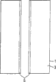
Fig. 6 is the plane graph of processing object thing that adopts the laser processing cutting of present embodiment.
Fig. 7 is the figure of the relation of the electric field strength in the laser processing of expression present embodiment and the size of breach point.
Fig. 8 is the sectional view of the processing object thing in the 1st operation of laser processing of present embodiment.
Fig. 9 is the sectional view of the processing object thing in the 2nd operation of laser processing of present embodiment.
Figure 10 is the sectional view of the processing object thing in the 3rd operation of laser processing of present embodiment.
Figure 11 is the sectional view of the processing object thing in the 4th operation of laser processing of present embodiment.
Figure 12 is the figure that show to adopt the section photo in the part of silicon substrate of laser processing cutting of present embodiment.
Figure 13 is the figure of the relation of the Wavelength of Laser in the laser processing of expression present embodiment and the transmitance of silicon substrate inside.
Figure 14 is the summary pie graph of the laser processing device relevant with embodiment 1.
Figure 15 is the flow chart that the explanation laser processing relevant with embodiment 1 used.
Figure 16 is the figure that show to form the semiconductor substrate after the operation in the cutting starting point field relevant with embodiment 1.
Figure 17 is that explanation attaches the figure that the operation of the diaphragm relevant with embodiment 1 is used.
Figure 18 is that the figure that the operation of the semiconductor substrate relevant with embodiment 1 is used is ground in explanation.
Figure 19 is that explanation attaches the figure that the operation of the film spreading relevant with embodiment 1 is used.
Figure 20 is that the figure that the operation of the diaphragm relevant with embodiment 1 is used is peelled off in explanation.
Figure 21 film spreading relevant with embodiment 1 that be explanation expansion sorts the figure that the operation of semiconductor chip is used.
Figure 22 is the figure that show to grind after the operation of the semiconductor substrate relevant with embodiment 1 in the chamfering of the edge part formation of the section rear side of semiconductor chip.
Figure 23 A is used for illustrating after the operation of grinding the semiconductor substrate relevant with embodiment 1 in the section of semiconductor chip residual when dissolving process field, the figure of the surperficial situation of breach arrival before the operation of grinding semiconductor substrate.
Figure 23 B is used for illustrating after the operation of grinding the semiconductor substrate relevant with embodiment 1 in the section of semiconductor chip residual when dissolving process field, the figure of the situation on the preceding breach no show surface of the operation of grinding semiconductor substrate.
Figure 24 A is used for illustrating after the operation of grinding the semiconductor substrate relevant with embodiment 1 in the section of semiconductor chip not residual when dissolving process field, the figure of the surperficial situation of breach arrival before the operation of grinding semiconductor substrate.
Figure 24 B is used for illustrating after the operation of grinding the semiconductor substrate relevant with embodiment 1 in the section of semiconductor chip not residual when dissolving process field, the figure of the situation on the preceding breach no show surface of the operation of grinding semiconductor substrate.
Figure 25 A is used for illustrating after the operation of grinding the semiconductor substrate relevant with embodiment 1 in that the edge part of the rear side of the section of semiconductor chip is residual when dissolving process field, the figure of the surperficial situation of breach arrival before the operation of grinding semiconductor substrate.
Figure 25 B is used for illustrating after the operation of grinding the semiconductor substrate relevant with embodiment 1 in that the edge part of the rear side of the section of semiconductor chip is residual when dissolving process field, the figure of the situation on the preceding breach no show surface of the operation of grinding semiconductor substrate.
Figure 26 A is the sectional view that grinds the periphery of the preceding semiconductor substrate of the operation of the semiconductor substrate relevant with embodiment 1.
Figure 26 B is the sectional view that grinds the periphery of the semiconductor substrate after the operation of the semiconductor substrate relevant with embodiment 1.
Figure 27 is the plane graph of the sapphire substrate relevant with embodiment 2.
Figure 28 is that explanation forms the sectional view that the operation in the cutting starting point field relevant with embodiment 2 is used.
Figure 29 is that explanation forms the sectional view that the operation of the function element relevant with embodiment 2 is used.
Figure 30 is that explanation attaches the sectional view that the operation of the diaphragm relevant with embodiment 2 is used.
Figure 31 is that the sectional view that the operation of the sapphire substrate relevant with embodiment 2 is used is ground in explanation.
Figure 32 is that explanation attaches the sectional view that the operation of the film spreading relevant with embodiment 2 is used.
Figure 33 sectional view that to be explanation use with the operation of the relevant diaphragm of ultraviolet irradiation and embodiment 2.
Figure 34 is that the sectional view that the operation of the diaphragm relevant with embodiment 2 is used is peelled off in explanation.
The figure that the operation of Figure 35 film spreading that to be explanation expansion relevant with embodiment 2, separating semiconductor chip is used.
Embodiment
Below, in conjunction with the accompanying drawings,, be elaborated to being applicable to embodiments of the present invention.The dividing method of the substrate of present embodiment has: make focal point polymerization and irradiating laser in the inside of substrate, utilize inner the formation by multi-photon of substrate to absorb the modified field that generates, form the operation in cutting starting point field; And after the operation that forms cutting starting point field, substrate is ground to the operation of the thickness of regulation.
At first,, particularly absorb, describe at multi-photon to forming the dividing method of the substrate of being implemented in the operation of cutting the starting point field.
The energy hv of photon is lower than the absorption band gap E of material
G, be transparent on the optics.Therefore, the condition of material production absorption is hv〉E
GBut, even be transparent on the optics, when the intensity of laser is very big, with nhv〉and E
GCondition (n=2,3,4 ...), can produce absorption in the material.This phenomenon is called as multi-photon and absorbs.If impulse wave, the intensity of laser is by the maximum power density (W/cm of laser at focal point
2) decision.For example, maximum power density is 1 * 10
8(W/cm
2) when above, produce multi-photon and absorb.Maximum power density can be tried to achieve by (energy of per 1 pulse of the laser on the focal point) ÷ (the Shu Guangdian basal area * pulse duration of laser).In addition, if continuous wave, the intensity of laser is by the electric field strength (W/cm of laser at focal point
2) decision.
With reference to Fig. 1~Fig. 6, describe utilizing such multi-photon laser processing principle that absorb, present embodiment.Fig. 1 is the plane graph of the substrate 1 in the laser processing, Fig. 2 is the sectional view along the II-II line of substrate 1 shown in Figure 1, Fig. 3 is the plane graph of the substrate 1 after the laser processing, Fig. 4 is the sectional view along the IV-IV line of substrate 1 shown in Figure 3, Fig. 5 is the sectional view along the V-V line of substrate 1 shown in Figure 3, and Fig. 6 is the plane graph of the substrate 1 that is cut.
As shown in Figures 1 and 2, on the surface 3 of substrate 1, the desirable cutting preset lines 5 of answering cutting substrate 1 is arranged.Cutting preset lines 5 is the hypothesis line that extends along linearity (also can on substrate 1 actual leads be used as cutting preset lines 5).The laser processing of present embodiment by producing the condition that multi-photon absorbs, makes focal point P polymerization in the inside of substrate 1, to substrate 1 irradiating laser L and form modified field 7.In addition, so-called focal point is the position of laser L optically focused.
By laser L being relatively moved, focal point P is moved along cutting preset lines 5 along cutting preset lines 5 (that is) along the arrow A direction.Like this,, only form modified field 7 along cutting preset lines 5, form cutting starting point fields (cutting reservations) 8 in this modified field 7 in the inside of substrate 1 as Fig. 3~shown in Figure 5.The laser processing of execution mode is not by substrate 1 absorption laser L, to cause substrate 1 heating, and form modified field 7.But, on substrate 1, see through laser L, in the inside of substrate 1 multi-photon taking place and absorb, and forms modified field 7.Therefore, the surface 3 of substrate 1 absorbs laser L hardly, so the surface 3 of substrate 1 can not dissolve.
To the cutting of substrate 1, if there is starting point at the position of cutting, substrate 1 just cuts from this starting point, so, as shown in Figure 6, can be with less power cutting substrate 1.Like this, just can cutting substrate 1, and unnecessary breaking can not take place on the surface 3 of substrate 1.
In addition, with cutting starting point field as aspect the cutting of the substrate of starting point, can consider following 2 kinds of situations.The first, after cutting starting point field forms, by on substrate, applying artificial power, the situation that makes substrate breakage, substrate is cut as starting point with cutting starting point field.This is the cutting of for example carrying out big thickness substrate.What is called applies artificial power and is meant, for example the cutting starting point field along substrate applies bending stress and shear stress on substrate, or substrate is applied the temperature difference thermal stress is taken place.It two is by forming cutting starting point field, as starting point, to break the final situation that substrate is cut naturally to the section direction (thickness direction) of substrate with cutting starting point field.This is when for example carrying out the cutting of little thickness substrate, can utilize the modified field of 1 row to form cutting starting point field; Under the situation of big thickness substrate, can utilize the modified field of the multiple row that forms on the thickness direction, form cutting starting point field.In addition, under this situation of breaking naturally, at cutting part, can on surface, not break corresponding to the part that does not form the position of cutting the starting point field in advance, only cut part, therefore, can control cutting effectively corresponding to the position that forms cutting starting point field.In recent years, the thickness of the substrate of silicon substrate etc. is more and more thinner, so controlled so good cutting method takes effect very much.
In the present embodiment, absorb the modified field that forms, following (1)~(3) kind situation is arranged by multi-photon.
(1) modified field is the situation that contains the breach field of one or more breaches
At substrate (for example by glass and LiTaO
3The piezoelectric that constitutes) inside makes the focal point polymerization, is 1 * 10 in the electric field strength of focal point
8(W/cm
2) more than, and pulse duration is an irradiating laser under the following condition of 1 μ s.The size of this pulse duration is when making multi-photon absorb constantly generation, on the surface of substrate meaningless damage not to take place, and can only form the condition in breach field in substrate inside.Thus, in the inner phenomenon that the so-called optical damage that causes takes place to be absorbed by multi-photon of substrate.Because this optical damage causes thermal strain in substrate inside, and form the breach field in the inside of substrate.As the higher limit of electric field strength, for example be 1 * 10
12(W/cm
2).The pulse duration preference is as being 1ns~200ns.In addition, forming of the breach field that absorb to generate by multi-photon, for example, be recorded in the 45th laser heat working research can collection of thesis (in December, 1998) " utilizing the inside line (marking) of the glass substrate that the solid state laser high order harmonic component carries out " of the 23rd page~the 28th page.
The present inventor tries to achieve the relation between the size of electric field strength and breach by experiment.Experiment condition is as follows.
(A) substrate: pyrex (pyrex) glass (thickness 700 μ m)
(B) laser
Light source: semiconductor laser excitation Nd:YAG laser
Wavelength: 1064nm
Laser spots basal area: 3.14 * 10
-8Cm
2
Vibration form: Q-switched pulse
Repetition rate: 100kHz
Pulse duration: 30ns
Output: output<1mJ/ pulse
Laser quality: TEM
00
Polarized light property: linear polarization
(C) optically focused lens
Transmitance to optical maser wavelength: 60%
(D) translational speed of the mounting table of mounting substrate: 100mm/ second
In addition, so-called laser quality TEM
00But, be expression optically focused height optically focused to the ripple of laser.
Fig. 7 is the figure of the above-mentioned result of experiment of expression.Transverse axis is a maximum power density, because laser is pulse laser, so electric field strength is represented with maximum power density.The longitudinal axis is represented the size of the breach part (breach point) that forms in the inside of substrate with the laser of 1 pulse.Breakdown point is assembled, and just becomes the breach field.The size of breach point is the size of the maximum length part in the shape of breach point.The data that stain among the figure is represented are optically focused with the multiplying power of lens (C) is 100 times, and opening number (NA) is 0.80 o'clock data.In addition, the data that the white point among the figure is represented are optically focused with the multiplying power of lens (C) is 50 times, and opening number (NA) is 0.55 o'clock data.As can be known, from maximum power density 10
11(W/cm
2) about beginning, the breach point takes place in the inside of substrate, also become big along with maximum power density becomes big, breach point.
Below, with reference to Fig. 8~Figure 11, in the laser processing of present embodiment, the principle of cutting substrate describes by forming the breach field.As shown in Figure 8, absorb under the condition that produces, make the inside of focal point P polymerization submounts 1,, form breach field 9 in inside along the cutting preset lines with laser L irradiated substrate 1 at multi-photon.Breach field 9 comprises one or more breaches.Form cutting starting point field in this breach field 9.As shown in Figure 9, be starting point (that is, being starting point) with breach field 9 with cutting starting point field, breach is further grown up, arrive the surface 3 and the back side 21 of substrate 1 as shown in figure 10, then as shown in figure 11, split cutting substrate 1 by making substrate 1.Sometimes arrive the surface of substrate and the breach at the back side and grow up naturally, then grow up sometimes by on substrate, applying power.
(2) modified field is the situation that dissolves process field
In substrate (for example such semi-conducting material of silicon) inside, make the focal point polymerization, be 1 * 10 in the electric field strength of focal point
8(W/cm
2) more than, and pulse duration is an irradiating laser under the following condition of 1 μ s.Thus, the inside of substrate absorbs by multi-photon, and the part is heated.By this heating, dissolve process field inner formation of substrate.What is called dissolves process field, in case be the field of solidifying again after dissolving, or is in the field of the state of dissolving, or the field of the state that solidifies again from the state of dissolving, and also can be described as the field of phase change and the field that crystal structure changes.In addition, dissolve process field, the field that also can be described as in single crystals structure, noncrystalline structure, the polycrystalline structure, certain structure is changed to other structure.That is, for example, be meant from single crystals structure be changed to noncrystalline structure the field, from the single crystals structure be changed to polycrystalline structure the field, be changed to the field that comprises noncrystalline structure and polycrystalline structure from the single crystals structure.When substrate is the silicon single crystal structure, dissolves process field and be for example uncrystalline silicon structure.As the higher limit of electric field strength, for example be 1 * 10
12(W/cm
2).The pulse duration preference is as being 1ns~200ns.
This case inventor by experiment, confirms in the inside of silicon substrate, dissolves process field and forms.Experiment condition is as follows.
(A) substrate: silicon substrate (thickness 350 μ m, 4 inches of external diameters)
(B) laser
Light source: semiconductor laser excitation Nd:YAG laser
Wavelength: 1064nm
Laser spots basal area: 3.14 * 10
-8Cm
2
Vibration form: Q-switched pulse
Repetition rate: 100kHz
Pulse duration: 30ns
Output: 20 μ J/ pulses
Laser quality: TEM
00
Polarized light property: linear polarization
(C) optically focused lens
Multiplying power: 50 times
N.A.:0.55
Transmitance to optical maser wavelength: 60%
(D) translational speed of the mounting table of mounting substrate: 100mm/ second
Section photo in the part of the silicon substrate of the laser processing cutting that Figure 12 represents to carry out with above-mentioned condition.Dissolve process field 13 in the formation of the inside of silicon substrate 11.In addition, dissolving process field 13 according to what above-mentioned condition formed, is about 100 μ m in the size on the thickness direction.
Describe dissolving process field 13 by multi-photon absorption formation.Figure 13 represents the relation of the transmitance of Wavelength of Laser and silicon substrate inside.Wherein, having represented to remove respectively the reflex components of the face side and the rear side of silicon substrate, only is inner transmitance.Above-mentioned relation when the thickness t that silicon substrate is shown is respectively 50 μ m, 100 μ m, 200 μ m, 500 μ m, 1000 μ m.
As can be known, for example, the Nd:YAG laser wavelength is that the thickness of 1064nm, silicon substrate is 500 μ m when following, and in the inside of silicon substrate, laser sees through more than 80%.Because the thickness of the silicon substrate 11 among Figure 12 is 350 μ m, make multi-photon absorb the process field 13 that dissolves that generates and be formed near the center of silicon substrate, that is, and apart from the part of surperficial 175 μ m.The transmitance of this moment is that the silicon substrate of 200 μ m is more than 90% when for referencial use with thickness, so, laser only is absorbed in the inside of silicon substrate 11 on a small quantity, nearly all see through.This means, be not at silicon substrate 11 absorbed inside laser, form in the inside of silicon substrate 11 and to dissolve process field 13 (promptly, dissolve process field by the common thermosetting of carrying out with laser that adds), absorb formation but dissolve process field 13 by multi-photon.Absorb to form by multi-photon and to dissolve process field, be found in " evaluation of the processing characteristics of the silicon that carries out with picosecond pulse laser " such as the 72nd page~the 73rd page of national congress of welding association speech summary the 66th collection (in April, 2000).
In addition, with dissolve cutting starting point field that process field forms as starting point, breach is taken place towards the section direction because its breach arrives the surface and the back side of silicon substrate, silicon substrate is cut.Sometimes, arrive the surface of silicon substrate and this breach at the back side and grow up naturally, then grow up sometimes by on silicon substrate, applying power.In addition, breach is from cutting starting point field, in the self-sown situation in the surface and the back side of silicon substrate, be the situation that process field grows up breach from the state of dissolving that dissolves that forms cutting starting point field nothing more than, or form the situation that process field makes breach grow up that dissolves in cutting starting point field when the state of dissolving solidifies again.Wherein, no matter any situation dissolves process field and all only forms in the inside of silicon substrate, on the cut surface after the cutting, as shown in figure 12, only forms in inside and dissolves process field.In the inside of substrate, when dissolving process field formation cutting starting point field, owing to be difficult to when cutting, therefore unnecessary the breaking of generation outside the line of cutting starting point field make cutting control become easy.
(3) modified field is the situation in variations in refractive index field
Inside at substrate (for example glass) makes the focal point polymerization, is 1 * 10 in the electric field strength of focal point
8(W/cm
2) more than, and pulse duration is under the following condition of 1 μ s, irradiating laser.Extremely short when pulse duration, when in the inside of substrate multi-photon taking place and absorbing, multi-photon absorbs not being converted into heat energy, causing that in the inside of substrate permanent structure such as the variation of ion valence mumber, crystallization or split pole orientation changes, and forms the variations in refractive index field of producing.As the higher limit of electric field strength, for example be 1 * 10
12(W/cm
2).The pulse duration preference is as being below the 1ns, and 1ps is with next better.By the multi-photon absorption variations in refractive index field is formed, for example, be recorded in " utilizing femtosecond laser to make the inner photoinduction structure that forms of glass " of the 105th page~the 111st page of the 42nd LASER HEAT working research meeting collection of thesis (the .11 month in 1997).
More than, to being described as the situation of utilizing multi-photon to absorb modified field (1)~(3) that form.But, as the crystal structure of considering substrate and fissility thereof etc., form cutting starting point field below resembling, then can cut the starting point field as starting point, with littler power, cutting substrate accurately with it.
That is, the substrate for the single crystals semiconductor by the diamond structure of silicon etc. constitutes preferably forms cutting starting point field in the direction along (111) face (the 1st splitting surface) and (110) face (the 2nd splitting surface).In addition, the substrate for the III-V compound semiconductor by the zincblende type structure of GaAs etc. constitutes preferably forms cutting starting point field in the direction along (110) face.In addition, for having sapphire (Al
2O
3) substrate of crystal structure of the hexagonal crystal system that waits, preferably be interarea, form cutting starting point field in direction along (1120) face (A face) or (1100) face (M face) with (0001) face (C face).
In addition, as along the direction that should form above-mentioned cutting starting point field the direction of (for example, along (111) face in the single crystal silicon substrate), or with the vertical direction of direction that should form cutting starting point field, on substrate, form the orientation plane, can will should be orientated the plane, on substrate, form easily and correctly along the cutting starting point field of the direction that should form cutting starting point field as benchmark.
Below, by embodiment, the present invention is made more specific description.
[embodiment 1]
At first, the operation that the inside of semiconductor substrate 1 is formed cutting starting point field describes.Earlier with reference to Figure 14, the laser processing device to using in the operation that forms cutting starting point field describes before explanation.Figure 14 is the summary pie graph of laser processing device 100.
Z-direction is the direction vertical with the surface 3 of semiconductor substrate 1, so, become the direction of the depth of focus of the laser L that incides semiconductor substrate 1.Like this, move in Z-direction, can make the interior polymeric of the focal point P of laser L at semiconductor substrate 1 by making Z axle stage 113.In addition, this focal point P is axial mobile at X (Y), is undertaken by utilizing X (Y) axle stage 109 (111) that semiconductor substrate 1 is moved at X (Y) direction of principal axis.
Lasing light emitter 101 is Nd:YAG lasers of pulsing laser.As the laser that can be used as lasing light emitter 101, also has Nd:YVO in addition
4Laser, Nd:YLF laser and titanium sapphire laser device.Dissolve the occasion of process field in formation, should adopt Nd:YAG laser, Nd:YVO
4Laser, Nd:YLF laser.Among the embodiment 1, use pulse laser to carry out the processing of semiconductor substrate 1, if but can make multi-photon absorb generation, good with continuous wave laser.
Below, with reference to Figure 14 and Figure 15, the operation that forms the cutting starting point field when using above-mentioned laser processing device 100 is described.Figure 15 is that explanation forms the flow chart that the operation in cutting starting point field is used.
Utilize not shown spectrophotometer etc. to measure the optical absorption characteristics of semiconductor substrate 1.According to this measurement result, selected take place the transparent wavelength of semiconductor substrate 1 or absorb the lasing light emitter 101 (S101) of the laser L of few wavelength.Then, measure the thickness of semiconductor substrate 1.According to the measurement result of thickness and the refractive index of semiconductor substrate 1, determine the amount of movement (S103) of semiconductor substrate 1 in Z-direction.This is the inside that is in semiconductor substrate 1 for the focal point P that makes laser L, with the focal point P of the laser L on the surface 3 that is positioned at semiconductor substrate 1 as the semiconductor substrate 1 of benchmark amount of movement in Z-direction.This amount of movement is imported into whole control part 127.
With semiconductor substrate 1 mounting on the mounting table 107 of laser processing device 100.And, from observing with light source 117 visible lights take place, to semiconductor substrate 1 throw light on (S105).Make a video recording in the surface 3 that utilizes 121 pairs of imaging apparatuss to comprise the semiconductor substrate 1 of illuminated cutting preset lines 5.Cutting preset lines 5 is the hypothesis lines of answering the expectation of cutting semiconductor substrate 1.Here, at each function element on the surface 3 that is formed at semiconductor substrate 1, dividing semiconductor substrate 1 obtains semiconductor chip, so cutting preset lines 5 is configured to the clathrate that can pass through between adjacent function element.Camera data by imaging apparatus 121 picked-ups is sent to camera data handling part 125.Camera data handling part 125 is according to this camera data, be positioned at surperficial 3 such focus datas perform calculations (S107) to observing focus with the visible light of light source 117.
This focus data is transferred to stage control part 115.Stage control part 115 according to this focus data, makes Z axle stage 113 move (S109) in Z-direction.Like this, observation is positioned at the surface 3 of semiconductor substrate 1 with the focus of the visible light of light source 117.In addition, camera data handling part 125 according to camera data, performs calculations to the expansion view data on the surface 3 that comprises the semiconductor substrate 1 that cuts preset lines 5.This enlarges view data, is transferred to monitor 129 through whole control part 127, with near this expanded view picture demonstration cutting preset lines 5 on the monitor 129.
The shifting momentum data of determining at step S103 is imported into whole control part 127 in advance, and this shifting momentum data is transferred to stage control part 115.Stage control part 115, according to this shifting momentum data, the inside in that the focal point P of laser L is positioned at semiconductor substrate 1 utilizes Z axle stage 113 to make semiconductor substrate 1 move (S111) on Z-direction.
Then, laser L is taken place, laser L is shone on the cutting preset lines 5 on surface 3 of semiconductor substrate 1 by lasing light emitter 101.Because the focal point P of laser L is positioned at the inside of semiconductor substrate 1, make to dissolve process field only in the formation of the inside of semiconductor substrate 1.And, X-axis stage 109 and Y-axis stage 111 can be moved along cutting preset lines 5, utilize the process field that dissolves along 5 formation of cutting preset lines, form along the cutting starting point field (S113) of cutting preset lines 5 in the inside of semiconductor substrate 1.
By above operation, the process that forms cutting starting point field is ended, in the semiconductor substrate 1 inner cutting starting point field that forms.When forming cutting starting point field in the inside of semiconductor substrate 1, can be starting point with cutting starting point field, at the thickness direction generation breach of semiconductor substrate 1 just with nature or less power.
According to embodiment 1, form in the operation in above-mentioned cutting starting point field, form cutting starting point field in position near surface 3 sides of the inside of semiconductor substrate 1, be starting point with this cutting starting point field, at the thickness direction generation breach of semiconductor substrate 1.Figure 16 is the figure of the semiconductor substrate 1 behind the displaying formation cutting starting point field.As shown in figure 16, be the breach 15 that starting point takes place at semiconductor substrate 1 with cutting starting point field, can form clathrate along the cutting preset lines, instrument arrives the surface 3 of semiconductor substrate 1, does not arrive the back side 21.That is,, will cut apart separately with the rectangular a plurality of function element 19 that are formed at semiconductor substrate 1 surface at the breach 15 that semiconductor substrate 1 takes place.In addition, utilize 15 cuttings of this breach semiconductor substrate 1 section mutually near.
In addition, so-called " forming cutting starting point field " in position near surface 3 sides of semiconductor substrate 1 inside, refer to, constitute the modified field that dissolves process field etc. in cutting starting point field, in that the side near surface 3 forms from the center (position of half of thickness) of the thickness direction of semiconductor substrate 1.Promptly, refer to, the center of the width in the modified field of the thickness direction of semiconductor substrate 1, be positioned at close surperficial 3 sides in center, rather than only refer to that the entire portion in modified field is positioned at the situation of surperficial 3 sides with respect to the center of the thickness direction of semiconductor substrate 1 from the thickness direction of semiconductor substrate 1.
Below, with reference to Figure 17~Figure 21, the operation of grinding semiconductor substrate 1 is described.Figure 17~Figure 21 is that explanation contains the figure that each operation of operation of grinding semiconductor substrate is used.In addition, among the embodiment 1, the thickness of semiconductor substrate can be from 350 μ m slimming to 50 μ m.
As shown in figure 17, paste diaphragm 20 on the surface 3 of the semiconductor substrate 1 after above-mentioned cutting starting point field forms.Keep film 20, when protection is formed at function element 19 on the surface 3 of semiconductor substrate 1, also be used to keep semiconductor substrate 1.Afterwards, as shown in figure 18, the back side 21 of cutting semiconductor substrate 1 is ground on the plane, this plane grind cut after, chemical etchings are implemented at the back side 21, with the semiconductor substrate 1 slim 50 μ m that turn to.Thus, that is, by the back side 21 of grinding semiconductor substrate 1, it is the breach 15 that starting point produces that the back side 21 reaches with cutting starting point field, semiconductor substrate 1 is divided into the semiconductor chip 25 that respectively has function element 19.In addition, as above-mentioned chemical etching, wet etching (HFHNO is for example arranged
3) or plasma etching (HBrCl
2) etc.
In addition, as shown in figure 19, paste film spreading 23,, afterwards, as shown in figure 20, peel off the diaphragm 20 of the function element 19 of pasting into the whole semiconductor chips 25 of covering to cover the back side of whole semiconductor chips 25.Then, as shown in figure 21, expansion film spreading 23 is separated from each other semiconductor chip 25, by absorption collet chuck (collet) 27 letter sorting semiconductor chips 25.
As mentioned above, according to the dividing method of the substrate of embodiment 1, in the element manufacturing operation, after forming function element 19 in the surface 3 at semiconductor substrate 1, but the back side 21 of grinding semiconductor substrate 1.In addition, the following effect that the operation by forming cutting starting point field and the operation of grinding semiconductor substrate realize respectively can obtain to high qualification rate slimming with the semiconductor chip corresponding with the miniaturization of semiconductor device 25.
Promptly, according to the operation that forms cutting starting point field, can prevent on the surface 3 of semiconductor substrate 1, generation departs from the breach cutting preset lines, unnecessary of the expectation that should cut off semiconductor substrate 1 or dissolves, and can prevent to produce unnecessary breach or dissolve in the semiconductor chip 25 that separating semiconductor substrate 1 obtains.
In addition, according to the operation in formation cutting starting point field,,, can increase from the quantity of the semiconductor chip 25 of 1 semiconductor substrate, 1 separation so the interval of adjacent functional element 19 is narrowed down owing to do not dissolve along the surface 3 of the semiconductor substrate 1 that cuts preset lines.
On the other hand, in the operation of grinding semiconductor substrate, after the inside at semiconductor substrate 1 forms cutting starting point field, the back side 21 of cutting semiconductor substrate 1 is ground on the plane, so that semiconductor substrate 1 becomes specific thickness, but this moment, even if the back side 21 reaches to cut the breach 15 that the starting point field is the starting point generation, also, grind the chip of cutting the semiconductor substrate 1 that causes or break so can prevent the plane because the section of the semiconductor substrate 1 that is cut off by this breach 15 is close to each other.Therefore, can prevent to produce chip or break, but slimming semiconductor substrate 1 and dividing semiconductor substrate 1.
Being close to also of section in the above-mentioned semiconductor substrate 1 can be achieved as follows effect,, prevents that grinding the swarf that grinds of cutting generation by the plane enters in the breach 15 that is, and prevents that the swarf that grinds of the semiconductor chip 25 that obtains by dividing semiconductor substrate 1 from polluting.Equally, being close to of the section in the semiconductor substrate 1, also can realize the effect of comparing, make the plane to grind to cut the chip of the semiconductor chip 25 that causes to splash and reduce with the situation of each semiconductor chip 25 each interval.That is, can use the film of inhibition confining force as diaphragm 20.
In addition, in the operation of grinding semiconductor substrate, because chemical etchings are implemented at the back side 21 of semiconductor substrate 1, so the further back side of the semiconductor chip 25 that obtains by dividing semiconductor substrate 1 of smoothing.And,, so as shown in figure 22,, and form chamfering 29 by the edge part of the rear side of this section of etching selectively only because be close to each other based on the section that with cutting starting point field is the semiconductor substrate 1 of the breach 15 that produces of starting point.Therefore, when the rupture strength that can make the semiconductor chip 25 that obtains by dividing semiconductor substrate 1 improves, can prevent to produce chip in the semiconductor chip 25 or break.
In addition, Figure 23 A~Figure 25 B illustrates the semiconductor chip 25 and the relation that dissolves process field 13 after the operation of grinding semiconductor substrate.In the semiconductor chip 25 shown in each figure, owing to have each effect described later, so can use respectively corresponding to various purposes.Here, Figure 23 A, Figure 24 A and Figure 25 A be before the operation of grinding semiconductor substrate, breach 15 arrives the situation at the back side 3 of semiconductor substrates 1, Figure 23 B, Figure 24 B and Figure 25 B be before the operation of grinding semiconductor substrate, the situation at the back side 3 of breach 15 no show semiconductor substrates 1.Under the situation of Figure 23 B, Figure 24 B and Figure 25 B, after the operation of grinding semiconductor substrate, breach 15 also arrives the back side 3 of semiconductor substrate 15.
Shown in Figure 23 A and Figure 23 B, the residual semiconductor chip 25 that dissolves process field 13 in section, its section is dissolved process field 13 and is protected, and the rupture strength of semiconductor chip 25 improves.
Shown in Figure 24 A and Figure 24 B, the not residual semiconductor chip 25 that dissolves process field 13 in section does not cause under the situation of influence effectively dissolving 13 pairs of semiconductor device of process field.
Shown in Figure 25 A and Figure 25 B; in the edge part of section rear side in the residual semiconductor chip 25 that dissolves process field 13; this edge part is dissolved process field 13 and protected, and is the same with the situation of the edge part of chamfering semiconductor chip 25, can prevent to produce chip in the edge part or break.
In addition, as Figure 23 A, Figure 24 A and Figure 25 A, with before the operation of grinding semiconductor substrate, breach 15 situation that arrives the back side 3 of semiconductor substrates 1 compares, shown in Figure 23 B, Figure 24 B and Figure 25 B, before the operation of grinding semiconductor substrate, under the situation at the back side 3 of breach 15 no show semiconductor substrates 1, the craspedodrome of the section of the semiconductor chip 25 that obtains after the operation of grinding semiconductor substrate further improves.
Therefore, much less, before the operation of grinding semiconductor substrate, breach 15 surface 3 that whether arrives semiconductor substrate 1 is with to dissolve process field 13 relevant to the degree of depth on surface 3, but also relevant with the size that dissolves process field 13.That is, if reduce to dissolve the size of process field 13, even if then dissolving process field 13 to the situation of the depth as shallow on surface 3, breach 15 does not arrive the surface 3 of semiconductor substrate 1 yet.The size that dissolves process field 13 for example can be controlled by the output of the pulse laser in the operation that forms cutting starting point field, if improve the output of pulse laser, then becomes big, if reduce the output of pulse laser, then diminishes.
In addition, the specific thickness of the semiconductor substrate 1 of slimming in the operation of consideration grinding semiconductor substrate, preferred (for example before the operation that forms cutting starting point field) in advance forms circle at the circumference (peripheral part) of the semiconductor substrate 1 of this specific thickness at least by chamfer machining.Figure 26 A and Figure 26 B are the sectional views of the circumference of the semiconductor substrate 1 before and after the grinding semiconductor substrate operation of embodiment 1.The thickness of the semiconductor substrate 1 shown in Figure 26 A before the grinding semiconductor substrate operation is 350 μ m, and the thickness of the semiconductor substrate 1 shown in Figure 26 B after the grinding semiconductor substrate operation is 50 μ m.Shown in Figure 26 A, at the circumference of semiconductor substrate 1, forming a plurality of (being 7 here) each thickness by chamfering in advance is the circle of 50 μ m,, the cross sectional shape of the circumference of semiconductor substrate 1 is formed waveform that is.Thus, shown in Figure 26 B, the circumference of the semiconductor substrate 1 after the operation of grinding semiconductor substrate 1, owing to become the state that forms circle by chamfering, produce chip or break so can prevent this circumference, and then by improving mechanical strength, can make that to handle transfiguration easy.
[embodiment 2]
The embodiment 2 of substrate cutting method of the present invention is described with reference to Figure 27~Figure 35.Embodiment 2 establishes substrate 1 for as the sapphire substrate (thickness is 450 μ m, and external diameter is 2 inches) of insulated substrate (below, in embodiment 2 " substrate 1 " is called " sapphire substrate 1 "), obtains constituting the situation of the semiconductor chip of light-emitting diode.In addition, Figure 28~Figure 35 is the sectional view along the XX-XX of sapphire substrate shown in Figure 27 1.
At first, as shown in figure 28, make focal point P optically focused in the inside of sapphire substrate 1, irradiating laser L forms modified field 7 in the inside of sapphire substrate 1.On the surface 3 of this sapphire substrate 1, in the operation afterwards that a plurality of function element 19 formation are rectangular, each function element 19 is carried out cutting apart of sapphire substrate 1.Therefore, consistent with the size of each function element 19, from surperficial 3 sides, be clathrate ground and set the cutting preset lines, form modified field 7 along this cutting preset lines, establish this modified field 7 and be cutting starting point field.
In addition, be 1 * 10 as if maximum power density at focal point P
8(W/cm
2) above, pulse duration is under the following condition of 1 μ s, to sapphire substrate 1 irradiating laser, then forms the breach field as modified field 7 (also form sometimes and dissolve process field).In addition, if (0001) face of sapphire substrate 1 is made as surface 3, along the direction of (1120) face and with the direction of this direction quadrature on form modified field 7, then in the operation of back, can be starting point with the cutting starting point field in this modified field 7, by littler power, come cutting substrate with high accuracy.This with along the direction of (1100) face and with the direction of this direction quadrature on to form modified field 7 the same.
After the cutting starting point field based on modified field 7 forms, as shown in figure 29, on the surface 3 of sapphire substrate 1, making n type gallium nitride compound semiconductor layer (below be called " n type layer ") 31 crystalline growths to thickness is 6 μ m, and, on n type layer 31, making p type gallium nitride compound semiconductor layer (below be called " p type layer ") 32 crystalline growths to thickness is 1 μ m.And, by n type layer 31 and p type layer 32 being etched into n type layer 31 midway, will form rectangular by a plurality of function element 19 that n type layer 31 and p type layer 32 constitute along forming cancellate modified field 7.
In addition, also can on the surface 3 of sapphire substrate 1, form after n type layer 31 and the p type layer 32, with focal point P optically focused in the inside of sapphire substrate 1, irradiating laser L, and form modified field 7 in the inside of sapphire substrate 1.In addition, irradiating laser L can carry out from surface 3 sides of sapphire substrate 1, also can 21 sides carry out from the back side.Because under the situation of surperficial 3 side irradiating laser L, laser L also has light transmission to sapphire substrate 1, n type layer 31 and p type layer 32, dissolves so can prevent n type layer 31 and p type layer 32 after forming n type layer 31 and p type layer 32.
After forming the function element 19 that constitutes by n type layer 31 and p type layer 32, as shown in figure 30, paste diaphragm 20 in the surface of sapphire substrate 13 sides.Diaphragm 20 also keeps sapphire substrate 1 when protection is formed at function element 19 on the surface 3 of sapphire substrate 1.Then, as shown in figure 31, the back side 21 of cutting sapphire substrate 1 is ground on the plane, is 150 μ m with the sapphire substrate 1 slim thickness that turns to.By grinding the back side 21 of sapphire substrate 1, cutting starting point field with modified field 7 is a starting point, produce breach 15, this breach 15 arrives the surface 3 and the back side 21 of sapphire substrate 1, sapphire substrate 1 is divided into the semiconductor chip 25 that respectively has the function element 19 that is made of n type layer 31 and p type layer 32.
In addition, shown in figure 32, paste extendible film spreading 23 with after the back side that covers whole semiconductor chips 25; as shown in figure 33, by to diaphragm 20 irradiation ultraviolet radiations, make UV cured resin curing as the adhesive linkage of diaphragm 20; as shown in figure 34, peel off diaphragm 20.Then, as shown in figure 35, expand film spreading 23 laterally, be separated from each other each semiconductor chip 25, by letter sorting semiconductor chips 25 such as absorption collet chucks.Afterwards, electrode is assemblied on the n type layer 31 and p type layer 32 of semiconductor chip 25, makes light-emitting diode.
As mentioned above, dividing method according to the substrate of embodiment 2, in the operation that forms cutting starting point field, because make focal point P optically focused in the inside of sapphire substrate 1, irradiating laser L, and make the inside of sapphire substrate 1 produce the phenomenon that so-called multi-photon absorbs, form modified field 7, so can pass through this modified field 7,, form cutting starting point field in the inside of sapphire substrate 1 along the cutting preset lines that should cut off the expectation of sapphire substrate 1.If form cutting starting point field in the inside of sapphire substrate 1,, be starting point with cutting starting point field, along the thickness direction generation breach 15 of sapphire substrate 1 then naturally or by less power.
In addition, in the operation of grinding sapphire substrate 1, after the inside at sapphire substrate 1 forms cutting starting point field, grind sapphire substrate 1, make sapphire substrate 1 become specific thickness, but even if arriving with cutting starting point field, abradant surface is the breach 15 that starting point produces this moment, also because the state of section for being close to each other of the sapphire substrate 1 that cuts off by this breach 15, so can prevent to grind the chip of the sapphire substrate 1 that causes or break.
Therefore, can prevent to produce chip or break, slimming sapphire substrate 1 and cut apart sapphire substrate 1, can obtain to high qualification rate the semiconductor chip 25 of slimming sapphire substrate 1.
In addition, even if cut apart, also can realize above-mentioned the same effect with the substrate under the situation of AlN substrate or GaAs substrate replacement sapphire substrate 1.
Utilizability on the industry
As mentioned above, according to the present invention, can prevent chip or break, the slimming substrate and Divide cutting board.
Claims (6)
1. the dividing method of a substrate is characterized in that,
Have: make the focal point polymerization in substrate inside, and be 1 * 10 at the maximum power density of focal point
8W/cm
2More than and pulse duration be irradiating laser under the following condition of 1 μ s, in the inner modified field that contains the breach field that forms of described substrate, utilize this modified field, in laser entrance face predetermined distance inboard apart from described substrate, along the cutting preset lines of described substrate, form the operation in cutting starting point field; With
After the operation that forms described cutting starting point field, grind the thickness of described substrate to regulation, cut apart the operation of described substrate along described cutting preset lines.
2. the dividing method of substrate according to claim 1 is characterized in that,
In the operation that forms described cutting starting point field, utilize described modified field, apart from the described predetermined distance of described laser entrance face inboard, be set at cancellate each cutting preset lines along described relatively substrate, form described cutting starting point field,
In the operation of grinding described substrate, grind the thickness of described substrate to described regulation, serve as the cutting starting point with described cutting starting point field, along described cutting preset lines, described substrate is divided into a plurality of chips.
3. the dividing method of substrate according to claim 1 and 2 is characterized in that,
Be formed with function element at described substrate surface,
In the operation of grinding described substrate, grind described substrate back.
4. the dividing method of substrate according to claim 3 is characterized in that,
The operation of grinding described substrate comprises the operation of described substrate back being implemented chemical etching.
5. the dividing method of substrate according to claim 1 and 2 is characterized in that,
In the operation of grinding described substrate, grind described substrate and make residual described modified field on described substrate.
6. the dividing method of substrate according to claim 1 and 2 is characterized in that,
In the operation of grinding described substrate, grinding described substrate and making in residual at least a portion on the described substrate is the breach that produces on the thickness direction at described substrate of starting point with described cutting starting point field, and on described substrate not residual described modified field.
Applications Claiming Priority (2)
| Application Number | Priority Date | Filing Date | Title |
|---|---|---|---|
| JP2002067289 | 2002-03-12 | ||
| JP200267289 | 2002-03-12 |
Related Parent Applications (1)
| Application Number | Title | Priority Date | Filing Date |
|---|---|---|---|
| CNB038058669A Division CN100355031C (en) | 2002-03-12 | 2003-03-06 | Method for deviding substrate |
Publications (2)
| Publication Number | Publication Date |
|---|---|
| CN1983556A CN1983556A (en) | 2007-06-20 |
| CN100485901C true CN100485901C (en) | 2009-05-06 |
Family
ID=27800279
Family Applications (5)
| Application Number | Title | Priority Date | Filing Date |
|---|---|---|---|
| CNB2006101643460A Expired - Lifetime CN100485901C (en) | 2002-03-12 | 2003-03-06 | Substrate dividing method |
| CNB038058669A Expired - Lifetime CN100355031C (en) | 2002-03-12 | 2003-03-06 | Method for deviding substrate |
| CNB2005100854440A Expired - Lifetime CN100355032C (en) | 2002-03-12 | 2003-03-06 | Substrate dividing method |
| CNB2006101643475A Expired - Lifetime CN100485902C (en) | 2002-03-12 | 2003-03-06 | Substrate dividing method |
| CN2007101823487A Expired - Lifetime CN101335235B (en) | 2002-03-12 | 2003-03-06 | Method for dicing substrate |
Family Applications After (4)
| Application Number | Title | Priority Date | Filing Date |
|---|---|---|---|
| CNB038058669A Expired - Lifetime CN100355031C (en) | 2002-03-12 | 2003-03-06 | Method for deviding substrate |
| CNB2005100854440A Expired - Lifetime CN100355032C (en) | 2002-03-12 | 2003-03-06 | Substrate dividing method |
| CNB2006101643475A Expired - Lifetime CN100485902C (en) | 2002-03-12 | 2003-03-06 | Substrate dividing method |
| CN2007101823487A Expired - Lifetime CN101335235B (en) | 2002-03-12 | 2003-03-06 | Method for dicing substrate |
Country Status (11)
| Country | Link |
|---|---|
| US (20) | US8268704B2 (en) |
| EP (7) | EP2400539B1 (en) |
| JP (7) | JP3762409B2 (en) |
| KR (2) | KR100715576B1 (en) |
| CN (5) | CN100485901C (en) |
| AT (3) | ATE534142T1 (en) |
| AU (1) | AU2003211763A1 (en) |
| DE (1) | DE60313900T2 (en) |
| ES (3) | ES2639733T3 (en) |
| TW (1) | TWI278027B (en) |
| WO (1) | WO2003077295A1 (en) |
Families Citing this family (306)
| Publication number | Priority date | Publication date | Assignee | Title |
|---|---|---|---|---|
| JP4659300B2 (en) | 2000-09-13 | 2011-03-30 | 浜松ホトニクス株式会社 | Laser processing method and semiconductor chip manufacturing method |
| TWI326626B (en) | 2002-03-12 | 2010-07-01 | Hamamatsu Photonics Kk | Laser processing method |
| EP2216128B1 (en) * | 2002-03-12 | 2016-01-27 | Hamamatsu Photonics K.K. | Method of cutting object to be processed |
| EP2400539B1 (en) | 2002-03-12 | 2017-07-26 | Hamamatsu Photonics K.K. | Substrate dividing method |
| TWI520269B (en) | 2002-12-03 | 2016-02-01 | Hamamatsu Photonics Kk | Cutting method of semiconductor substrate |
| FR2852250B1 (en) | 2003-03-11 | 2009-07-24 | Jean Luc Jouvin | PROTECTIVE SHEATH FOR CANNULA, AN INJECTION KIT COMPRISING SUCH ANKLE AND NEEDLE EQUIPPED WITH SUCH ANKLE |
| US8685838B2 (en) | 2003-03-12 | 2014-04-01 | Hamamatsu Photonics K.K. | Laser beam machining method |
| JP4342832B2 (en) | 2003-05-16 | 2009-10-14 | 株式会社東芝 | Semiconductor device and manufacturing method thereof |
| JP4494728B2 (en) * | 2003-05-26 | 2010-06-30 | 株式会社ディスコ | Non-metallic substrate division method |
| EP2269765B1 (en) * | 2003-07-18 | 2014-10-15 | Hamamatsu Photonics K.K. | Cut semiconductor chip |
| JP4563097B2 (en) | 2003-09-10 | 2010-10-13 | 浜松ホトニクス株式会社 | Semiconductor substrate cutting method |
| JP4598407B2 (en) | 2004-01-09 | 2010-12-15 | 浜松ホトニクス株式会社 | Laser processing method and laser processing apparatus |
| JP4601965B2 (en) | 2004-01-09 | 2010-12-22 | 浜松ホトニクス株式会社 | Laser processing method and laser processing apparatus |
| JP4509578B2 (en) | 2004-01-09 | 2010-07-21 | 浜松ホトニクス株式会社 | Laser processing method and laser processing apparatus |
| CN100428418C (en) * | 2004-02-09 | 2008-10-22 | 株式会社迪斯科 | Method for cutting wafer |
| JP4082400B2 (en) * | 2004-02-19 | 2008-04-30 | セイコーエプソン株式会社 | Electro-optical device manufacturing method, electro-optical device, and electronic apparatus |
| JP2005252126A (en) * | 2004-03-08 | 2005-09-15 | Disco Abrasive Syst Ltd | Method of working wafer |
| JP4584607B2 (en) * | 2004-03-16 | 2010-11-24 | 浜松ホトニクス株式会社 | Processing object cutting method |
| JP4536407B2 (en) * | 2004-03-30 | 2010-09-01 | 浜松ホトニクス株式会社 | Laser processing method and object to be processed |
| KR101336523B1 (en) | 2004-03-30 | 2013-12-03 | 하마마츠 포토닉스 가부시키가이샤 | Laser processing method and semiconductor chip |
| JP4694795B2 (en) * | 2004-05-18 | 2011-06-08 | 株式会社ディスコ | Wafer division method |
| US7459377B2 (en) * | 2004-06-08 | 2008-12-02 | Panasonic Corporation | Method for dividing substrate |
| JP4733934B2 (en) * | 2004-06-22 | 2011-07-27 | 株式会社ディスコ | Wafer processing method |
| JP4447392B2 (en) * | 2004-07-23 | 2010-04-07 | 株式会社ディスコ | Wafer dividing method and dividing apparatus |
| JP4200177B2 (en) * | 2004-08-06 | 2008-12-24 | 浜松ホトニクス株式会社 | Laser processing method and semiconductor device |
| JP2006108532A (en) * | 2004-10-08 | 2006-04-20 | Disco Abrasive Syst Ltd | Method of grinding wafer |
| JP4781661B2 (en) * | 2004-11-12 | 2011-09-28 | 浜松ホトニクス株式会社 | Laser processing method |
| JP4565977B2 (en) * | 2004-11-25 | 2010-10-20 | 株式会社東京精密 | Film peeling method and film peeling apparatus |
| JP4762653B2 (en) * | 2005-09-16 | 2011-08-31 | 浜松ホトニクス株式会社 | Laser processing method and laser processing apparatus |
| JP2007134454A (en) * | 2005-11-09 | 2007-05-31 | Toshiba Corp | Method of manufacturing semiconductor device |
| KR100858983B1 (en) * | 2005-11-16 | 2008-09-17 | 가부시키가이샤 덴소 | Semiconductor device and dicing method for semiconductor substrate |
| JP4907965B2 (en) * | 2005-11-25 | 2012-04-04 | 浜松ホトニクス株式会社 | Laser processing method |
| JP4804911B2 (en) * | 2005-12-22 | 2011-11-02 | 浜松ホトニクス株式会社 | Laser processing equipment |
| JP4907984B2 (en) * | 2005-12-27 | 2012-04-04 | 浜松ホトニクス株式会社 | Laser processing method and semiconductor chip |
| JP2007235068A (en) * | 2006-03-03 | 2007-09-13 | Tokyo Seimitsu Co Ltd | Wafer machining method |
| JP2007235069A (en) | 2006-03-03 | 2007-09-13 | Tokyo Seimitsu Co Ltd | Wafer machining method |
| JP2007317747A (en) * | 2006-05-23 | 2007-12-06 | Seiko Epson Corp | Substrate dividing method and method of manufacturing liquid injection head |
| US7897487B2 (en) * | 2006-07-03 | 2011-03-01 | Hamamatsu Photonics K.K. | Laser processing method and chip |
| JP5183892B2 (en) | 2006-07-03 | 2013-04-17 | 浜松ホトニクス株式会社 | Laser processing method |
| JP4954653B2 (en) | 2006-09-19 | 2012-06-20 | 浜松ホトニクス株式会社 | Laser processing method |
| US8188404B2 (en) * | 2006-09-19 | 2012-05-29 | Hamamatsu Photonics K.K. | Laser processing method and laser processing apparatus |
| JP5101073B2 (en) * | 2006-10-02 | 2012-12-19 | 浜松ホトニクス株式会社 | Laser processing equipment |
| JP5132911B2 (en) * | 2006-10-03 | 2013-01-30 | 浜松ホトニクス株式会社 | Laser processing method |
| JP4964554B2 (en) * | 2006-10-03 | 2012-07-04 | 浜松ホトニクス株式会社 | Laser processing method |
| EP2070636B1 (en) | 2006-10-04 | 2015-08-05 | Hamamatsu Photonics K.K. | Laser processing method |
| JP4306717B2 (en) * | 2006-11-09 | 2009-08-05 | セイコーエプソン株式会社 | Method for manufacturing silicon device and method for manufacturing liquid jet head |
| US8530784B2 (en) * | 2007-02-01 | 2013-09-10 | Orbotech Ltd. | Method and system of machining using a beam of photons |
| US7888236B2 (en) * | 2007-05-14 | 2011-02-15 | Taiwan Semiconductor Manufacturing Co., Ltd. | Semiconductor device and fabrication methods thereof |
| US8603351B2 (en) * | 2007-05-25 | 2013-12-10 | Hamamatsu Photonics K.K. | Working method for cutting |
| JP5336054B2 (en) * | 2007-07-18 | 2013-11-06 | 浜松ホトニクス株式会社 | Processing information supply system provided with processing information supply device |
| JP2009032970A (en) * | 2007-07-27 | 2009-02-12 | Rohm Co Ltd | Method of manufacturing nitride semiconductor element |
| JP5449665B2 (en) | 2007-10-30 | 2014-03-19 | 浜松ホトニクス株式会社 | Laser processing method |
| JP5054496B2 (en) * | 2007-11-30 | 2012-10-24 | 浜松ホトニクス株式会社 | Processing object cutting method |
| JP5134928B2 (en) * | 2007-11-30 | 2013-01-30 | 浜松ホトニクス株式会社 | Workpiece grinding method |
| JP5160868B2 (en) * | 2007-12-06 | 2013-03-13 | 株式会社ディスコ | Method for forming a modified layer on a substrate |
| JP2009290148A (en) * | 2008-06-02 | 2009-12-10 | Disco Abrasive Syst Ltd | Method of dividing wafer |
| JP5231136B2 (en) * | 2008-08-22 | 2013-07-10 | 株式会社ディスコ | Processing method of optical device wafer |
| JP5692969B2 (en) | 2008-09-01 | 2015-04-01 | 浜松ホトニクス株式会社 | Aberration correction method, laser processing method using this aberration correction method, laser irradiation method using this aberration correction method, aberration correction apparatus, and aberration correction program |
| DE102008052006B4 (en) | 2008-10-10 | 2018-12-20 | 3D-Micromac Ag | Method and device for the production of samples for transmission electron microscopy |
| CN102203943B (en) * | 2008-10-29 | 2013-07-31 | 欧瑞康太阳能股份公司(特吕巴赫) | Method for dividing a semiconductor film formed on a substrate into plural regions by multiple laser beam irradiation |
| KR101539246B1 (en) * | 2008-11-10 | 2015-07-24 | 삼성전자 주식회사 | Fabricating method of the light emitting device for improving light extraction efficiency and light emitting device fabricated by the method |
| JP5254761B2 (en) | 2008-11-28 | 2013-08-07 | 浜松ホトニクス株式会社 | Laser processing equipment |
| JP5241525B2 (en) | 2009-01-09 | 2013-07-17 | 浜松ホトニクス株式会社 | Laser processing equipment |
| JP5241527B2 (en) | 2009-01-09 | 2013-07-17 | 浜松ホトニクス株式会社 | Laser processing equipment |
| JP5632751B2 (en) | 2009-02-09 | 2014-11-26 | 浜松ホトニクス株式会社 | Processing object cutting method |
| CN102326232B (en) * | 2009-02-25 | 2016-01-20 | 日亚化学工业株式会社 | The manufacture method of semiconductor element |
| CN102317030B (en) | 2009-04-07 | 2014-08-20 | 浜松光子学株式会社 | Laser machining device and laser machining method |
| JP5491761B2 (en) | 2009-04-20 | 2014-05-14 | 浜松ホトニクス株式会社 | Laser processing equipment |
| JP5307612B2 (en) * | 2009-04-20 | 2013-10-02 | 株式会社ディスコ | Processing method of optical device wafer |
| JP5340808B2 (en) * | 2009-05-21 | 2013-11-13 | 株式会社ディスコ | Laser processing method of semiconductor wafer |
| JP5340806B2 (en) * | 2009-05-21 | 2013-11-13 | 株式会社ディスコ | Laser processing method of semiconductor wafer |
| JP5340807B2 (en) * | 2009-05-21 | 2013-11-13 | 株式会社ディスコ | Processing method of semiconductor wafer |
| JP5537081B2 (en) | 2009-07-28 | 2014-07-02 | 浜松ホトニクス株式会社 | Processing object cutting method |
| CN102470484B (en) | 2009-08-11 | 2015-09-30 | 浜松光子学株式会社 | Laser processing device and laser processing |
| JP5379604B2 (en) | 2009-08-21 | 2013-12-25 | 浜松ホトニクス株式会社 | Laser processing method and chip |
| JP2011077235A (en) * | 2009-09-30 | 2011-04-14 | Nitto Denko Corp | Pressure-sensitive adhesive sheet for retaining element, and method of manufacturing element |
| JP5595716B2 (en) * | 2009-11-18 | 2014-09-24 | 株式会社ディスコ | Processing method of optical device wafer |
| JP2011114018A (en) * | 2009-11-24 | 2011-06-09 | Disco Abrasive Syst Ltd | Method of manufacturing optical device |
| JP5709370B2 (en) * | 2009-11-26 | 2015-04-30 | 株式会社ディスコ | Cutting apparatus and cutting method |
| JP5149888B2 (en) | 2009-12-04 | 2013-02-20 | リンテック株式会社 | Stealth dicing adhesive sheet and method for manufacturing semiconductor device |
| DE102010009015A1 (en) * | 2010-02-24 | 2011-08-25 | OSRAM Opto Semiconductors GmbH, 93055 | Method for producing a plurality of optoelectronic semiconductor chips |
| JP5710133B2 (en) * | 2010-03-16 | 2015-04-30 | 株式会社ディスコ | How to divide work |
| JP2011200926A (en) | 2010-03-26 | 2011-10-13 | Mitsuboshi Diamond Industrial Co Ltd | Laser beam machining method and brittle material substrate |
| JP5840828B2 (en) * | 2010-04-12 | 2016-01-06 | 株式会社ディスコ | Processing method of optical device wafer |
| JP5670647B2 (en) | 2010-05-14 | 2015-02-18 | 浜松ホトニクス株式会社 | Processing object cutting method |
| US8950217B2 (en) | 2010-05-14 | 2015-02-10 | Hamamatsu Photonics K.K. | Method of cutting object to be processed, method of cutting strengthened glass sheet and method of manufacturing strengthened glass member |
| JP5549403B2 (en) * | 2010-06-16 | 2014-07-16 | 富士通セミコンダクター株式会社 | Manufacturing method of semiconductor device |
| US8828260B2 (en) | 2010-07-26 | 2014-09-09 | Hamamatsu Photonics K.K. | Substrate processing method |
| US8841213B2 (en) | 2010-07-26 | 2014-09-23 | Hamamatsu Photonics K.K. | Method for manufacturing interposer |
| WO2012014709A1 (en) | 2010-07-26 | 2012-02-02 | 浜松ホトニクス株式会社 | Laser processing method |
| JP5653110B2 (en) | 2010-07-26 | 2015-01-14 | 浜松ホトニクス株式会社 | Chip manufacturing method |
| KR102000031B1 (en) | 2010-07-26 | 2019-07-15 | 하마마츠 포토닉스 가부시키가이샤 | Laser processing method |
| EP2600411B1 (en) | 2010-07-26 | 2019-08-21 | Hamamatsu Photonics K.K. | Method for manufacturing light-absorbing substrate and method for manufacturing die for manufacturing light-absorbing substrate |
| JP5574866B2 (en) | 2010-07-26 | 2014-08-20 | 浜松ホトニクス株式会社 | Laser processing method |
| KR20130106770A (en) | 2010-07-26 | 2013-09-30 | 하마마츠 포토닉스 가부시키가이샤 | Method for manufacturing semiconductor device |
| JP5693074B2 (en) | 2010-07-26 | 2015-04-01 | 浜松ホトニクス株式会社 | Laser processing method |
| EP2599577A4 (en) | 2010-07-26 | 2016-06-15 | Hamamatsu Photonics Kk | Laser processing method |
| JP5702556B2 (en) | 2010-07-26 | 2015-04-15 | 浜松ホトニクス株式会社 | Laser processing method |
| JP5389266B2 (en) | 2010-07-26 | 2014-01-15 | 浜松ホトニクス株式会社 | Substrate processing method |
| JP2012033668A (en) * | 2010-07-30 | 2012-02-16 | Mitsuboshi Diamond Industrial Co Ltd | Laser processing method |
| JP5584560B2 (en) * | 2010-08-31 | 2014-09-03 | 三星ダイヤモンド工業株式会社 | Laser scribing method |
| US8722516B2 (en) | 2010-09-28 | 2014-05-13 | Hamamatsu Photonics K.K. | Laser processing method and method for manufacturing light-emitting device |
| JP2012089709A (en) * | 2010-10-20 | 2012-05-10 | Disco Abrasive Syst Ltd | Method for dividing workpiece |
| KR101688591B1 (en) | 2010-11-05 | 2016-12-22 | 삼성전자주식회사 | Method of manufacturing the semiconductor chip |
| JP2012104644A (en) * | 2010-11-10 | 2012-05-31 | Tokyo Seimitsu Co Ltd | Wafer cutting method and wafer cutting device |
| JP5733954B2 (en) * | 2010-11-15 | 2015-06-10 | 株式会社ディスコ | Method for dividing optical device wafer |
| JP5758116B2 (en) * | 2010-12-16 | 2015-08-05 | 株式会社ディスコ | Split method |
| JP5819605B2 (en) * | 2010-12-17 | 2015-11-24 | 株式会社ディスコ | Substrate dividing method |
| JP5480169B2 (en) * | 2011-01-13 | 2014-04-23 | 浜松ホトニクス株式会社 | Laser processing method |
| JP5503580B2 (en) * | 2011-03-17 | 2014-05-28 | 古河電気工業株式会社 | Adhesive tape for brittle wafer processing |
| US8538576B2 (en) * | 2011-04-05 | 2013-09-17 | Asm Technology Singapore Pte. Ltd. | Method of configuring a dicing device, and a dicing apparatus for dicing a workpiece |
| JP5753734B2 (en) * | 2011-05-19 | 2015-07-22 | 日本特殊陶業株式会社 | Wiring board, multi-cavity wiring board, and manufacturing method thereof |
| JP2013008831A (en) * | 2011-06-24 | 2013-01-10 | Disco Abrasive Syst Ltd | Processing method of wafer |
| EP2723506B1 (en) * | 2011-06-27 | 2017-02-15 | Koninklijke Philips N.V. | Ultrasound transducer assembly and method of manufacturing the same |
| RU2469433C1 (en) * | 2011-07-13 | 2012-12-10 | Юрий Георгиевич Шретер | Method for laser separation of epitaxial film or layer of epitaxial film from growth substrate of epitaxial semiconductor structure (versions) |
| JP2013042119A (en) * | 2011-07-21 | 2013-02-28 | Hamamatsu Photonics Kk | Light-emitting element manufacturing method |
| US8575758B2 (en) * | 2011-08-04 | 2013-11-05 | Texas Instruments Incorporated | Laser-assisted cleaving of a reconstituted wafer for stacked die assemblies |
| US8569086B2 (en) * | 2011-08-24 | 2013-10-29 | Taiwan Semiconductor Manufacturing Company, Ltd. | Semiconductor device and method of dicing semiconductor devices |
| CN102990227A (en) * | 2011-09-08 | 2013-03-27 | 技鼎股份有限公司 | Single-wavelength multilayer laser machining method |
| US20130095581A1 (en) * | 2011-10-18 | 2013-04-18 | Taiwan Semiconductor Manufacturing Company, Ltd. | Thick window layer led manufacture |
| CN102515495B (en) * | 2011-12-13 | 2015-01-21 | 意力(广州)电子科技有限公司 | Panel glass multimode processing method and semi-finished product processed by adopting method |
| KR101909633B1 (en) | 2011-12-30 | 2018-12-19 | 삼성전자 주식회사 | Method of cutting light emitting device chip wafer using laser scribing |
| JP2013157455A (en) * | 2012-01-30 | 2013-08-15 | Hamamatsu Photonics Kk | Method for manufacturing semiconductor device |
| JP6012185B2 (en) * | 2012-01-30 | 2016-10-25 | 浜松ホトニクス株式会社 | Manufacturing method of semiconductor device |
| JP2013157449A (en) * | 2012-01-30 | 2013-08-15 | Hamamatsu Photonics Kk | Method for manufacturing semiconductor device |
| JP5969214B2 (en) * | 2012-01-30 | 2016-08-17 | 浜松ホトニクス株式会社 | Manufacturing method of semiconductor device |
| WO2013117667A1 (en) * | 2012-02-10 | 2013-08-15 | Arges Gmbh | Laser contrasting method and apparatus for carrying out a contrasting method |
| JP5988601B2 (en) * | 2012-02-13 | 2016-09-07 | 株式会社ディスコ | Method for dividing optical device wafer |
| KR101883843B1 (en) * | 2012-02-16 | 2018-08-01 | 엘지이노텍 주식회사 | Method for forming a cleaved facet of semiconductor device |
| JP5988603B2 (en) * | 2012-02-17 | 2016-09-07 | 株式会社ディスコ | Method for dividing optical device wafer |
| US10052848B2 (en) * | 2012-03-06 | 2018-08-21 | Apple Inc. | Sapphire laminates |
| JP2013219076A (en) * | 2012-04-04 | 2013-10-24 | Disco Abrasive Syst Ltd | Method for processing optical device wafer |
| US9847445B2 (en) * | 2012-04-05 | 2017-12-19 | Koninklijke Philips N.V. | LED thin-film device partial singulation prior to substrate thinning or removal |
| JP2013219271A (en) * | 2012-04-11 | 2013-10-24 | Disco Abrasive Syst Ltd | Method for processing optical device wafer |
| JP6011002B2 (en) * | 2012-04-23 | 2016-10-19 | セイコーエプソン株式会社 | Manufacturing method of liquid ejecting head and manufacturing method of liquid ejecting apparatus |
| TWI581451B (en) * | 2012-05-21 | 2017-05-01 | 晶元光電股份有限公司 | Optoelectronic device and method for manufacturing the same |
| US9266192B2 (en) | 2012-05-29 | 2016-02-23 | Electro Scientific Industries, Inc. | Method and apparatus for processing workpieces |
| CN103456847B (en) * | 2012-06-01 | 2017-12-26 | 晶元光电股份有限公司 | Photoelectric cell and its manufacture method |
| JP6001931B2 (en) * | 2012-06-14 | 2016-10-05 | 株式会社ディスコ | Wafer processing method |
| JP2014011381A (en) * | 2012-07-02 | 2014-01-20 | Disco Abrasive Syst Ltd | Wafer processing method |
| JP2014013807A (en) * | 2012-07-04 | 2014-01-23 | Disco Abrasive Syst Ltd | Wafer processing method |
| KR20140006484A (en) * | 2012-07-05 | 2014-01-16 | 삼성전자주식회사 | Fabrication method of semiconductor light emitting device |
| JP6013858B2 (en) * | 2012-10-01 | 2016-10-25 | 株式会社ディスコ | Wafer processing method |
| JP6087565B2 (en) | 2012-10-03 | 2017-03-01 | 株式会社ディスコ | Grinding apparatus and grinding method |
| JP2014082317A (en) * | 2012-10-16 | 2014-05-08 | Disco Abrasive Syst Ltd | Wafer processing method |
| JP6026222B2 (en) * | 2012-10-23 | 2016-11-16 | 株式会社ディスコ | Wafer processing method |
| JP6064519B2 (en) * | 2012-10-29 | 2017-01-25 | 三星ダイヤモンド工業株式会社 | Laser processing apparatus and processing condition setting method for patterned substrate |
| US20140145294A1 (en) * | 2012-11-28 | 2014-05-29 | Nxp B.V. | Wafer separation |
| US8809166B2 (en) * | 2012-12-20 | 2014-08-19 | Nxp B.V. | High die strength semiconductor wafer processing method and system |
| JP6062287B2 (en) * | 2013-03-01 | 2017-01-18 | 株式会社ディスコ | Wafer processing method |
| JP6113529B2 (en) | 2013-03-05 | 2017-04-12 | 株式会社ディスコ | Wafer processing method |
| JP6158551B2 (en) * | 2013-03-26 | 2017-07-05 | 株式会社ディスコ | Wafer dividing method |
| ES2959429T3 (en) | 2013-04-04 | 2024-02-26 | Lpkf Laser & Electronics Se | Procedure for separating a substrate |
| CN103400779B (en) * | 2013-07-09 | 2014-09-03 | 程君 | Manufacturing method of semiconductor display panel |
| KR102231083B1 (en) | 2013-07-22 | 2021-03-23 | 루미리즈 홀딩 비.브이. | Method of separating light emitting devices formed on a substrate wafer |
| US20150034613A1 (en) * | 2013-08-02 | 2015-02-05 | Rofin-Sinar Technologies Inc. | System for performing laser filamentation within transparent materials |
| US9102011B2 (en) | 2013-08-02 | 2015-08-11 | Rofin-Sinar Technologies Inc. | Method and apparatus for non-ablative, photoacoustic compression machining in transparent materials using filamentation by burst ultrafast laser pulses |
| CN103441104B (en) * | 2013-08-29 | 2016-06-22 | 华进半导体封装先导技术研发中心有限公司 | Method for cutting wafer |
| CN103441103B (en) * | 2013-08-29 | 2016-06-01 | 华进半导体封装先导技术研发中心有限公司 | Method for cutting wafer |
| JP6232230B2 (en) * | 2013-08-30 | 2017-11-15 | 株式会社ディスコ | Wafer processing method |
| JP6257979B2 (en) * | 2013-09-24 | 2018-01-10 | 株式会社ディスコ | Wafer dividing method |
| DE102014013107A1 (en) | 2013-10-08 | 2015-04-09 | Siltectra Gmbh | Novel wafer manufacturing process |
| US10017410B2 (en) | 2013-10-25 | 2018-07-10 | Rofin-Sinar Technologies Llc | Method of fabricating a glass magnetic hard drive disk platter using filamentation by burst ultrafast laser pulses |
| US10005152B2 (en) | 2013-11-19 | 2018-06-26 | Rofin-Sinar Technologies Llc | Method and apparatus for spiral cutting a glass tube using filamentation by burst ultrafast laser pulses |
| US11053156B2 (en) | 2013-11-19 | 2021-07-06 | Rofin-Sinar Technologies Llc | Method of closed form release for brittle materials using burst ultrafast laser pulses |
| DE102013223637B4 (en) | 2013-11-20 | 2018-02-01 | Trumpf Laser- Und Systemtechnik Gmbh | A method of treating a laser transparent substrate for subsequently separating the substrate |
| US10144088B2 (en) | 2013-12-03 | 2018-12-04 | Rofin-Sinar Technologies Llc | Method and apparatus for laser processing of silicon by filamentation of burst ultrafast laser pulses |
| US9154678B2 (en) | 2013-12-11 | 2015-10-06 | Apple Inc. | Cover glass arrangement for an electronic device |
| JP6341554B2 (en) * | 2013-12-19 | 2018-06-13 | 国立大学法人東京工業大学 | Manufacturing method of semiconductor device |
| US9209082B2 (en) | 2014-01-03 | 2015-12-08 | International Business Machines Corporation | Methods of localized hardening of dicing channel by applying localized heat in wafer kerf |
| JP6251574B2 (en) | 2014-01-14 | 2017-12-20 | 株式会社ディスコ | Cutting method |
| JP6230422B2 (en) * | 2014-01-15 | 2017-11-15 | 株式会社ディスコ | Wafer processing method |
| US9938187B2 (en) | 2014-02-28 | 2018-04-10 | Rofin-Sinar Technologies Llc | Method and apparatus for material processing using multiple filamentation of burst ultrafast laser pulses |
| JP2015185831A (en) * | 2014-03-26 | 2015-10-22 | 旭化成株式会社 | Nitride semiconductor light emitting element |
| JP2015195106A (en) * | 2014-03-31 | 2015-11-05 | 株式会社ジャパンディスプレイ | Organic el display device and method for manufacturing the same |
| JP6324796B2 (en) * | 2014-04-21 | 2018-05-16 | 株式会社ディスコ | Single crystal substrate processing method |
| KR102378063B1 (en) | 2014-05-23 | 2022-03-23 | 린텍 가부시키가이샤 | Composite sheet for forming protective film |
| KR102355108B1 (en) | 2014-06-10 | 2022-01-24 | 린텍 가부시키가이샤 | Dicing sheet |
| JP6305272B2 (en) | 2014-08-14 | 2018-04-04 | 株式会社ディスコ | Transport device |
| CN106660333B (en) | 2014-08-22 | 2018-11-06 | 琳得科株式会社 | The manufacturing method of protective film formation piece and semiconductor chip with protective film |
| US9601437B2 (en) * | 2014-09-09 | 2017-03-21 | Nxp B.V. | Plasma etching and stealth dicing laser process |
| DE102014116958B9 (en) | 2014-11-19 | 2017-10-05 | Trumpf Laser- Und Systemtechnik Gmbh | Optical system for beam shaping of a laser beam, laser processing system, method for material processing and use of a common elongated focus zone for laser material processing |
| WO2016079275A1 (en) | 2014-11-19 | 2016-05-26 | Trumpf Laser- Und Systemtechnik Gmbh | System for asymmetric optical beam shaping |
| DE102014116957A1 (en) | 2014-11-19 | 2016-05-19 | Trumpf Laser- Und Systemtechnik Gmbh | Optical system for beam shaping |
| JP6399913B2 (en) | 2014-12-04 | 2018-10-03 | 株式会社ディスコ | Wafer generation method |
| JP2016115800A (en) * | 2014-12-15 | 2016-06-23 | 株式会社ディスコ | Processing method for wafer |
| DE102014119581A1 (en) * | 2014-12-23 | 2016-06-23 | Wink Stanzwerkzeuge Gmbh & Co. Kg | Process for the production of steel sheets for stamped sheets |
| JP6399923B2 (en) * | 2014-12-24 | 2018-10-03 | 株式会社ディスコ | Laser processing method for plate |
| SG11201705157WA (en) | 2014-12-25 | 2017-07-28 | Denka Company Ltd | Adhesive sheet for laser dicing and method for manufacturing semiconductor device |
| JP6391471B2 (en) * | 2015-01-06 | 2018-09-19 | 株式会社ディスコ | Wafer generation method |
| CN106132627B (en) * | 2015-01-13 | 2018-09-07 | 罗芬-新纳技术有限责任公司 | For carrying out scribing and the then method and system of progress chemical etching to fragile material |
| JP6438791B2 (en) * | 2015-02-06 | 2018-12-19 | リンテック株式会社 | Manufacturing method of semiconductor device |
| JP6395632B2 (en) | 2015-02-09 | 2018-09-26 | 株式会社ディスコ | Wafer generation method |
| JP6395633B2 (en) | 2015-02-09 | 2018-09-26 | 株式会社ディスコ | Wafer generation method |
| JP6495056B2 (en) * | 2015-03-06 | 2019-04-03 | 株式会社ディスコ | Single crystal substrate processing method |
| JP2016171214A (en) | 2015-03-12 | 2016-09-23 | 株式会社ディスコ | Processing method of single crystal substrate |
| US9873170B2 (en) | 2015-03-24 | 2018-01-23 | Nichia Corporation | Method of manufacturing light emitting element |
| JP6146455B2 (en) * | 2015-03-24 | 2017-06-14 | 日亜化学工業株式会社 | Method for manufacturing light emitting device |
| JP6429715B2 (en) | 2015-04-06 | 2018-11-28 | 株式会社ディスコ | Wafer generation method |
| JP6425606B2 (en) | 2015-04-06 | 2018-11-21 | 株式会社ディスコ | Wafer production method |
| JP6494382B2 (en) | 2015-04-06 | 2019-04-03 | 株式会社ディスコ | Wafer generation method |
| DE102015004603A1 (en) | 2015-04-09 | 2016-10-13 | Siltectra Gmbh | Combined wafer fabrication process with laser treatment and temperature-induced stresses |
| JP6456766B2 (en) * | 2015-05-08 | 2019-01-23 | 株式会社ディスコ | Wafer processing method |
| JP6472333B2 (en) | 2015-06-02 | 2019-02-20 | 株式会社ディスコ | Wafer generation method |
| JP2017005158A (en) | 2015-06-12 | 2017-01-05 | 株式会社ディスコ | Method for grinding rear surface of wafer |
| US10406634B2 (en) | 2015-07-01 | 2019-09-10 | Apple Inc. | Enhancing strength in laser cutting of ceramic components |
| JP6560040B2 (en) | 2015-07-06 | 2019-08-14 | 株式会社ディスコ | Wafer processing method |
| JP6482423B2 (en) | 2015-07-16 | 2019-03-13 | 株式会社ディスコ | Wafer generation method |
| JP6472347B2 (en) | 2015-07-21 | 2019-02-20 | 株式会社ディスコ | Thinning method of wafer |
| JP6482425B2 (en) | 2015-07-21 | 2019-03-13 | 株式会社ディスコ | Thinning method of wafer |
| JP6727948B2 (en) * | 2015-07-24 | 2020-07-22 | ソニーセミコンダクタソリューションズ株式会社 | Imaging device and manufacturing method |
| JP6300763B2 (en) | 2015-08-03 | 2018-03-28 | 株式会社ディスコ | Workpiece processing method |
| JP5900811B2 (en) * | 2015-08-28 | 2016-04-06 | 株式会社東京精密 | Semiconductor substrate cleaving method |
| JP6523882B2 (en) * | 2015-09-02 | 2019-06-05 | 株式会社ディスコ | Wafer processing method |
| CN107922259B (en) * | 2015-09-04 | 2021-05-07 | Agc株式会社 | Method for producing glass plate, method for producing glass article, and apparatus for producing glass article |
| JP6605277B2 (en) | 2015-09-29 | 2019-11-13 | 浜松ホトニクス株式会社 | Laser processing method and laser processing apparatus |
| JP6605278B2 (en) | 2015-09-29 | 2019-11-13 | 浜松ホトニクス株式会社 | Laser processing method |
| JP6542630B2 (en) | 2015-09-29 | 2019-07-10 | 浜松ホトニクス株式会社 | Laser processing method and laser processing apparatus |
| JP6625854B2 (en) * | 2015-10-06 | 2019-12-25 | 株式会社ディスコ | Optical device wafer processing method |
| JP2017131949A (en) * | 2016-01-28 | 2017-08-03 | 浜松ホトニクス株式会社 | Laser processing apparatus and laser processing method |
| JP6644580B2 (en) * | 2016-02-24 | 2020-02-12 | 浜松ホトニクス株式会社 | Laser beam irradiation device and laser beam irradiation method |
| JP6608732B2 (en) * | 2016-03-01 | 2019-11-20 | 株式会社ディスコ | Wafer processing method |
| JP6157668B2 (en) * | 2016-03-02 | 2017-07-05 | 株式会社東京精密 | Wafer processing method and processing apparatus |
| JP6128666B2 (en) * | 2016-03-02 | 2017-05-17 | 株式会社東京精密 | Semiconductor substrate cleaving method and cleaving apparatus |
| JP6666173B2 (en) * | 2016-03-09 | 2020-03-13 | 株式会社ディスコ | Laser processing equipment |
| CN108712938B (en) * | 2016-03-10 | 2021-06-25 | 浜松光子学株式会社 | Laser irradiation apparatus and laser irradiation method |
| JP6690983B2 (en) | 2016-04-11 | 2020-04-28 | 株式会社ディスコ | Wafer generation method and actual second orientation flat detection method |
| JP6633446B2 (en) * | 2016-04-27 | 2020-01-22 | 株式会社ディスコ | Wafer processing method |
| JP6636384B2 (en) | 2016-05-13 | 2020-01-29 | 株式会社ディスコ | Wafer processing method |
| JP6723644B2 (en) | 2016-05-16 | 2020-07-15 | 株式会社ディスコ | Expandable seat |
| JP6341959B2 (en) | 2016-05-27 | 2018-06-13 | 浜松ホトニクス株式会社 | Manufacturing method of Fabry-Perot interference filter |
| TWI717519B (en) | 2016-05-27 | 2021-02-01 | 日商濱松赫德尼古斯股份有限公司 | Manufacturing method of Fabry-Peru interference filter |
| JP6710457B2 (en) | 2016-06-01 | 2020-06-17 | 株式会社ディスコ | Expanded sheet, method for manufacturing expanded sheet, and method for expanding expanded sheet |
| DE102016111144B4 (en) * | 2016-06-17 | 2024-03-07 | Tdk Electronics Ag | Method for producing a variety of components and components |
| JP2016201551A (en) * | 2016-06-20 | 2016-12-01 | 株式会社東京精密 | Minute cracking forming method and minute cracking forming device of semiconductor substrate |
| JP6103739B2 (en) * | 2016-06-20 | 2017-03-29 | 株式会社東京精密 | Wafer processing method and wafer processing apparatus |
| JP6276332B2 (en) * | 2016-07-04 | 2018-02-07 | 株式会社東京精密 | Wafer processing system |
| JP6713212B2 (en) * | 2016-07-06 | 2020-06-24 | 株式会社ディスコ | Method for manufacturing semiconductor device chip |
| JP6745165B2 (en) | 2016-08-09 | 2020-08-26 | 株式会社ディスコ | Wafer processing method |
| JP6276347B2 (en) * | 2016-08-18 | 2018-02-07 | 株式会社東京精密 | Wafer processing system |
| JP6276357B2 (en) * | 2016-09-21 | 2018-02-07 | 株式会社東京精密 | Wafer processing method |
| JP6276356B2 (en) * | 2016-09-21 | 2018-02-07 | 株式会社東京精密 | Wafer processing method |
| JP6746211B2 (en) | 2016-09-21 | 2020-08-26 | 株式会社ディスコ | Wafer processing method |
| JP6775880B2 (en) | 2016-09-21 | 2020-10-28 | 株式会社ディスコ | Wafer processing method |
| JP6821245B2 (en) * | 2016-10-11 | 2021-01-27 | 株式会社ディスコ | Wafer processing method |
| KR102447761B1 (en) | 2016-11-02 | 2022-09-27 | 린텍 가부시키가이샤 | dicing sheet |
| JP6986393B2 (en) * | 2016-11-15 | 2021-12-22 | ビアメカニクス株式会社 | Substrate processing method |
| JP6814613B2 (en) | 2016-11-28 | 2021-01-20 | 株式会社ディスコ | Wafer processing method |
| DE102016224978B4 (en) * | 2016-12-14 | 2022-12-29 | Disco Corporation | substrate processing method |
| CN106654063B (en) * | 2016-12-28 | 2019-11-19 | 武汉华星光电技术有限公司 | The production method of flexible OLED display panel |
| JP6197970B2 (en) * | 2017-01-06 | 2017-09-20 | 株式会社東京精密 | Division start point formation method and division start point formation apparatus |
| DE102017200631B4 (en) | 2017-01-17 | 2022-12-29 | Disco Corporation | Method of processing a substrate |
| JP6817822B2 (en) * | 2017-01-18 | 2021-01-20 | 株式会社ディスコ | Processing method |
| JP6276437B2 (en) * | 2017-02-16 | 2018-02-07 | 株式会社東京精密 | Method and system for forming thin chip with high bending strength |
| JP6858587B2 (en) | 2017-02-16 | 2021-04-14 | 株式会社ディスコ | Wafer generation method |
| JP6649308B2 (en) * | 2017-03-22 | 2020-02-19 | キオクシア株式会社 | Semiconductor device and manufacturing method thereof |
| JP6957187B2 (en) * | 2017-04-18 | 2021-11-02 | 浜松ホトニクス株式会社 | Chip manufacturing method and silicon chip |
| JP6951124B2 (en) | 2017-05-23 | 2021-10-20 | 株式会社ディスコ | Processing method |
| JP2017224826A (en) * | 2017-06-27 | 2017-12-21 | 株式会社東京精密 | Method and system for forming thin chip with high bending strength |
| DE102017212858A1 (en) * | 2017-07-26 | 2019-01-31 | Disco Corporation | Method for processing a substrate |
| JP6980444B2 (en) * | 2017-07-28 | 2021-12-15 | 浜松ホトニクス株式会社 | Manufacturing method of laminated element |
| JP6941022B2 (en) * | 2017-10-06 | 2021-09-29 | 株式会社ディスコ | Expansion method and expansion device |
| KR102450776B1 (en) * | 2017-10-27 | 2022-10-05 | 삼성전자주식회사 | Laser processing method, substrate dicing method, and substrate processing apparatus for performing the same |
| JP2018046291A (en) * | 2017-11-22 | 2018-03-22 | 株式会社東京精密 | Manufacturing system and manufacturing method for thin chip with high rupture strength |
| JP6925945B2 (en) * | 2017-11-30 | 2021-08-25 | 株式会社ディスコ | Wafer processing method |
| CN108147363B (en) * | 2017-12-22 | 2019-09-20 | 烟台睿创微纳技术股份有限公司 | A kind of separation method of MEMS wafer chip |
| JP2018142717A (en) * | 2018-04-20 | 2018-09-13 | 株式会社東京精密 | Wafer processing method and wafer processing system |
| DE102018111227A1 (en) * | 2018-05-09 | 2019-11-14 | Osram Opto Semiconductors Gmbh | Method for cutting an epitaxially grown semiconductor body and semiconductor chip |
| JP2018133593A (en) * | 2018-05-22 | 2018-08-23 | 株式会社東京精密 | Wafer processing method and wafer processing system |
| JP6593663B2 (en) * | 2018-06-28 | 2019-10-23 | 株式会社東京精密 | Wafer processing method and wafer processing system |
| WO2020004210A1 (en) * | 2018-06-29 | 2020-01-02 | リンテック株式会社 | Method for producing semiconductor chip and method for producing semiconductor device |
| JP7154860B2 (en) | 2018-07-31 | 2022-10-18 | 株式会社ディスコ | Wafer processing method |
| JP6703073B2 (en) * | 2018-10-03 | 2020-06-03 | 株式会社東京精密 | Wafer processing method and wafer processing system |
| JP6703072B2 (en) * | 2018-10-03 | 2020-06-03 | 株式会社東京精密 | Wafer processing method and wafer processing system |
| US11664276B2 (en) * | 2018-11-30 | 2023-05-30 | Texas Instruments Incorporated | Front side laser-based wafer dicing |
| TWI681241B (en) * | 2018-12-04 | 2020-01-01 | 友達光電股份有限公司 | Manufacturing method for display device and display device utilized thereof |
| US10562130B1 (en) | 2018-12-29 | 2020-02-18 | Cree, Inc. | Laser-assisted method for parting crystalline material |
| US10576585B1 (en) | 2018-12-29 | 2020-03-03 | Cree, Inc. | Laser-assisted method for parting crystalline material |
| US11024501B2 (en) | 2018-12-29 | 2021-06-01 | Cree, Inc. | Carrier-assisted method for parting crystalline material along laser damage region |
| JP7176695B2 (en) * | 2019-03-07 | 2022-11-22 | 株式会社Nsc | Glass substrate manufacturing method |
| JP2019096910A (en) * | 2019-03-13 | 2019-06-20 | 株式会社東京精密 | Laser processing system |
| JP2019096911A (en) * | 2019-03-13 | 2019-06-20 | 株式会社東京精密 | Laser processing system |
| JP2019161232A (en) * | 2019-04-22 | 2019-09-19 | 株式会社東京精密 | Laser processing system |
| JP2019169719A (en) * | 2019-04-25 | 2019-10-03 | 株式会社東京精密 | Laser processing system |
| US10611052B1 (en) | 2019-05-17 | 2020-04-07 | Cree, Inc. | Silicon carbide wafers with relaxed positive bow and related methods |
| JP2019192937A (en) * | 2019-07-05 | 2019-10-31 | 株式会社東京精密 | Wafer processing system and wafer processing method |
| KR20210020683A (en) * | 2019-08-16 | 2021-02-24 | 삼성전자주식회사 | Semiconductor substrate and method of dicing the same |
| JP7358193B2 (en) | 2019-10-28 | 2023-10-10 | 株式会社ディスコ | Wafer processing method |
| JP2020025142A (en) * | 2019-11-18 | 2020-02-13 | 株式会社東京精密 | Wafer processing device and wafer processing method for obtaining chip with high transverse intensity |
| JP6653943B1 (en) * | 2019-12-25 | 2020-02-26 | 株式会社東京精密 | Laser processing equipment for semiconductor wafers to obtain chips with high bending strength |
| JP7290843B2 (en) * | 2020-01-24 | 2023-06-14 | 株式会社東京精密 | Crack growth device and crack growth method |
| JP2020080409A (en) * | 2020-01-24 | 2020-05-28 | 株式会社東京精密 | Laser processing system and laser processing method |
| JP2020074454A (en) * | 2020-01-24 | 2020-05-14 | 株式会社東京精密 | Laser processing system and laser processing method for improving chip strength |
| JP7217409B2 (en) * | 2020-01-24 | 2023-02-03 | 株式会社東京精密 | Crack growth device and crack growth method |
| JP7446673B2 (en) | 2020-02-21 | 2024-03-11 | 株式会社ディスコ | Wafer processing method |
| JP7446672B2 (en) | 2020-02-21 | 2024-03-11 | 株式会社ディスコ | Wafer processing method |
| JP7460274B2 (en) | 2020-02-21 | 2024-04-02 | 株式会社ディスコ | Wafer processing method |
| CN111298853B (en) * | 2020-02-27 | 2021-08-10 | 西人马联合测控(泉州)科技有限公司 | Chip cutting and forming method and wafer |
| JP7370902B2 (en) | 2020-02-28 | 2023-10-30 | 株式会社ディスコ | Crack detection method |
| JP7401372B2 (en) | 2020-03-26 | 2023-12-19 | 株式会社ディスコ | Wafer processing method |
| CN111451646A (en) * | 2020-04-24 | 2020-07-28 | 苏州镭明激光科技有限公司 | Processing technology for laser invisible cutting of wafer |
| JP7442939B2 (en) | 2020-07-02 | 2024-03-05 | 株式会社ディスコ | Wafer inspection method |
| CN113371989A (en) * | 2021-05-26 | 2021-09-10 | 苏州镭明激光科技有限公司 | Splitting method and splitting device for semiconductor chip |
| JP2023023328A (en) | 2021-08-05 | 2023-02-16 | 株式会社ディスコ | Inspection device |
| CN114815340A (en) * | 2022-05-19 | 2022-07-29 | 豪威半导体(上海)有限责任公司 | LCOS display and manufacturing method thereof |
| US20230411169A1 (en) * | 2022-06-15 | 2023-12-21 | Western Digital Technologies, Inc. | Semiconductor wafer thinned by horizontal stealth lasing |
Family Cites Families (452)
| Publication number | Priority date | Publication date | Assignee | Title |
|---|---|---|---|---|
| US456233A (en) * | 1891-07-21 | Lubricator | ||
| US3448510A (en) | 1966-05-20 | 1969-06-10 | Western Electric Co | Methods and apparatus for separating articles initially in a compact array,and composite assemblies so formed |
| JPS4624989Y1 (en) | 1967-08-31 | 1971-08-28 | ||
| US3629545A (en) | 1967-12-19 | 1971-12-21 | Western Electric Co | Laser substrate parting |
| GB1246481A (en) | 1968-03-29 | 1971-09-15 | Pilkington Brothers Ltd | Improvements in or relating to the cutting of glass |
| US3613974A (en) | 1969-03-10 | 1971-10-19 | Saint Gobain | Apparatus for cutting glass |
| JPS4812599Y1 (en) | 1969-03-24 | 1973-04-05 | ||
| JPS4812599B1 (en) | 1969-07-09 | 1973-04-21 | ||
| US3610871A (en) | 1970-02-19 | 1971-10-05 | Western Electric Co | Initiation of a controlled fracture |
| US3626141A (en) | 1970-04-30 | 1971-12-07 | Quantronix Corp | Laser scribing apparatus |
| US3824678A (en) | 1970-08-31 | 1974-07-23 | North American Rockwell | Process for laser scribing beam lead semiconductor wafers |
| US3909582A (en) | 1971-07-19 | 1975-09-30 | American Can Co | Method of forming a line of weakness in a multilayer laminate |
| US3790744A (en) | 1971-07-19 | 1974-02-05 | American Can Co | Method of forming a line of weakness in a multilayer laminate |
| US3790051A (en) | 1971-09-07 | 1974-02-05 | Radiant Energy Systems | Semiconductor wafer fracturing technique employing a pressure controlled roller |
| US3800991A (en) | 1972-04-10 | 1974-04-02 | Ppg Industries Inc | Method of and an apparatus for cutting glass |
| SE403280B (en) | 1972-10-12 | 1978-08-07 | Glaverbel | KIT AND DEVICE TO CUT GLASS OR GLASS CRYSTALLINIC MATERIAL ALONG A DETERMINED LINE |
| JPS5628630B2 (en) | 1973-05-30 | 1981-07-03 | ||
| JPS5628630Y2 (en) | 1974-10-30 | 1981-07-07 | ||
| JPS5157283A (en) | 1974-11-15 | 1976-05-19 | Nippon Electric Co | Handotaikibanno bunkatsuhoho |
| US3970819A (en) | 1974-11-25 | 1976-07-20 | International Business Machines Corporation | Backside laser dicing system |
| US4046985A (en) | 1974-11-25 | 1977-09-06 | International Business Machines Corporation | Semiconductor wafer alignment apparatus |
| US4190759A (en) | 1975-08-27 | 1980-02-26 | Hitachi, Ltd. | Processing of photomask |
| US4027137A (en) | 1975-09-17 | 1977-05-31 | International Business Machines Corporation | Laser drilling nozzle |
| NL7609815A (en) | 1976-09-03 | 1978-03-07 | Philips Nv | PROCESS FOR MANUFACTURING A SEMI-CONDUCTOR DEVICE AND SEMI-CONDUCTOR DEVICE MANUFACTURED BY THE PROCESS. |
| JPS5333050A (en) | 1976-09-08 | 1978-03-28 | Hitachi Ltd | Production of semiconductor element |
| US4092518A (en) | 1976-12-07 | 1978-05-30 | Laser Technique S.A. | Method of decorating a transparent plastics material article by means of a laser beam |
| JPS53141573A (en) | 1977-05-16 | 1978-12-09 | Toshiba Corp | Pellet dividing method of semiconductor wafer |
| JPS53141673A (en) | 1977-05-17 | 1978-12-09 | Seiko Epson Corp | Digital alarm watch with remaining time display using analogical pattern |
| JPS53114347A (en) | 1977-12-07 | 1978-10-05 | Toshiba Corp | Working method for semiconductor device |
| JPS54161349U (en) | 1978-04-29 | 1979-11-12 | ||
| JPS54161349A (en) | 1978-06-10 | 1979-12-20 | Nippon Telegr & Teleph Corp <Ntt> | Three-dimensional cross type waveguide passage |
| US4242152A (en) | 1979-05-14 | 1980-12-30 | National Semiconductor Corporation | Method for adjusting the focus and power of a trimming laser |
| JPS5628630A (en) | 1979-08-16 | 1981-03-20 | Kawasaki Steel Corp | Temperature controlling method of high temperature high pressure reacting cylinder |
| JPS6041478B2 (en) | 1979-09-10 | 1985-09-17 | 富士通株式会社 | Manufacturing method of semiconductor laser device |
| JPS5676522A (en) | 1979-11-29 | 1981-06-24 | Toshiba Corp | Formation of semiconductor thin film |
| JPS6043236B2 (en) | 1980-03-12 | 1985-09-27 | 松下電器産業株式会社 | Laser processing method |
| JPS56169347A (en) | 1980-05-31 | 1981-12-26 | Toshiba Corp | Laser scribing device |
| US4336439A (en) | 1980-10-02 | 1982-06-22 | Coherent, Inc. | Method and apparatus for laser scribing and cutting |
| US4392476A (en) | 1980-12-23 | 1983-07-12 | Lazare Kaplan & Sons, Inc. | Method and apparatus for placing identifying indicia on the surface of precious stones including diamonds |
| DE3110235A1 (en) | 1981-03-17 | 1982-10-21 | Trumpf GmbH & Co, 7257 Ditzingen | "METHOD AND DEVICE FOR FLAME-CUTTING BY MEANS OF A LASER BEAM" |
| JPS5836939A (en) | 1981-08-26 | 1983-03-04 | Toshiba Corp | Cutting method for glass wafer |
| JPS5854648A (en) | 1981-09-28 | 1983-03-31 | Nippon Kogaku Kk <Nikon> | Positioning device |
| JPS5857767A (en) | 1981-10-01 | 1983-04-06 | Matsushita Electric Ind Co Ltd | Laser device |
| US4475027A (en) | 1981-11-17 | 1984-10-02 | Allied Corporation | Optical beam homogenizer |
| JPS58181492A (en) | 1982-04-02 | 1983-10-24 | グレタ−ク・アクチエンゲゼルシヤフト | Method and device for focussing optical beam having coherence |
| JPS58171783A (en) | 1982-04-02 | 1983-10-08 | Hitachi Ltd | Magnetic bubble memory chip |
| JPS5916344A (en) | 1982-07-19 | 1984-01-27 | Toshiba Corp | Device of wafer scribing with laser |
| JPS6054151B2 (en) | 1982-10-22 | 1985-11-28 | 株式会社東芝 | Laser cutting method |
| JPS5976687U (en) | 1982-11-17 | 1984-05-24 | プレスコンクリ−ト工業株式会社 | precast gutter |
| JPS59141233A (en) | 1983-02-02 | 1984-08-13 | Nec Corp | Manufacture of semiconductor device |
| JPS59150691A (en) | 1983-02-15 | 1984-08-28 | Matsushita Electric Ind Co Ltd | Laser working machine |
| JPH0611071B2 (en) * | 1983-09-07 | 1994-02-09 | 三洋電機株式会社 | Method for dividing compound semiconductor substrate |
| US4546231A (en) | 1983-11-14 | 1985-10-08 | Group Ii Manufacturing Ltd. | Creation of a parting zone in a crystal structure |
| JPS59130438A (en) | 1983-11-28 | 1984-07-27 | Hitachi Ltd | Method for separating plates |
| US4650619A (en) | 1983-12-29 | 1987-03-17 | Toshiba Ceramics Co., Ltd. | Method of machining a ceramic member |
| JPS60144985A (en) | 1983-12-30 | 1985-07-31 | Fujitsu Ltd | Manufacture of semiconductor light-emitting element |
| JPS60167351A (en) | 1984-02-09 | 1985-08-30 | Mitsubishi Electric Corp | Manufacture of hybrid integrated circuit device |
| US4562333A (en) | 1984-09-04 | 1985-12-31 | General Electric Company | Stress assisted cutting of high temperature embrittled materials |
| DE3575805D1 (en) | 1984-10-11 | 1990-03-08 | Hitachi Ltd | BRACKET FOR OPTICAL LENS. |
| JPS6196439A (en) | 1984-10-17 | 1986-05-15 | Toray Ind Inc | Lens defect inspecting instrument |
| JPS61112345A (en) | 1984-11-07 | 1986-05-30 | Toshiba Corp | Manufacture of semiconductor device |
| JPS61121453A (en) | 1984-11-19 | 1986-06-09 | Matsushita Electric Ind Co Ltd | Braking and expanding process of fragile thin sheet |
| JPS61220339A (en) | 1985-03-26 | 1986-09-30 | Nippon Telegr & Teleph Corp <Ntt> | Control of characteristics of semiconductor material |
| JPS61229487A (en) | 1985-04-03 | 1986-10-13 | Sasaki Glass Kk | Method for cutting glass by laser beam |
| US4689491A (en) | 1985-04-19 | 1987-08-25 | Datasonics Corp. | Semiconductor wafer scanning system |
| JPS624341A (en) | 1985-06-29 | 1987-01-10 | Toshiba Corp | Manufacture of semiconductor device |
| KR890004933B1 (en) * | 1985-07-31 | 1989-11-30 | 가부시기가이샤 히다찌세이사꾸쇼 | Turbo molecular pump |
| JPS6240986A (en) | 1985-08-20 | 1987-02-21 | Fuji Electric Corp Res & Dev Ltd | Laser beam machining method |
| JPH0732281B2 (en) | 1985-10-25 | 1995-04-10 | 株式会社日立製作所 | Cleaving device and cleaving method |
| AU584563B2 (en) | 1986-01-31 | 1989-05-25 | Ciba-Geigy Ag | Laser marking of ceramic materials, glazes, glass ceramics and glasses |
| JPH0750811B2 (en) | 1986-06-17 | 1995-05-31 | 松下電器産業株式会社 | Cleaving method of semiconductor laser |
| JPS6384789A (en) | 1986-09-26 | 1988-04-15 | Semiconductor Energy Lab Co Ltd | Light working method |
| FR2605310B1 (en) | 1986-10-16 | 1992-04-30 | Comp Generale Electricite | METHOD FOR REINFORCING CERAMIC WORKPIECES BY LASER TREATMENT |
| US4815854A (en) | 1987-01-19 | 1989-03-28 | Nec Corporation | Method of alignment between mask and semiconductor wafer |
| JPH0688149B2 (en) | 1987-03-04 | 1994-11-09 | 株式会社半導体エネルギ−研究所 | Light processing method |
| JPS63278692A (en) | 1987-05-07 | 1988-11-16 | D S Sukiyanaa:Kk | Automatic focusing mechanism in laser beam machine |
| JPS63293939A (en) | 1987-05-27 | 1988-11-30 | Hitachi Ltd | Manufacture of semiconductor integrated circuit device |
| JPS6438209A (en) | 1987-08-04 | 1989-02-08 | Nec Corp | Preparation of semiconductor device |
| JPS6438209U (en) | 1987-08-29 | 1989-03-07 | ||
| JPH01112130A (en) | 1987-10-26 | 1989-04-28 | Matsushita Electric Ind Co Ltd | Method for evaluating infrared optical fiber |
| US5300942A (en) | 1987-12-31 | 1994-04-05 | Projectavision Incorporated | High efficiency light valve projection system with decreased perception of spaces between pixels and/or hines |
| JPH01108508U (en) | 1988-01-16 | 1989-07-21 | ||
| US4981525A (en) | 1988-02-19 | 1991-01-01 | Sanyo Electric Co., Ltd. | Photovoltaic device |
| JPH0256987A (en) | 1988-02-23 | 1990-02-26 | Mitsubishi Electric Corp | Mounting method of hybrid integrated circuit |
| FR2627409A1 (en) | 1988-02-24 | 1989-08-25 | Lectra Systemes Sa | LASER CUTTING APPARATUS WITH A FUME EXHAUST DEVICE |
| JPH01225509A (en) | 1988-03-04 | 1989-09-08 | Sumitomo Electric Ind Ltd | Dividing method for semiconductor base |
| JPH01225510A (en) | 1988-03-04 | 1989-09-08 | Sumitomo Electric Ind Ltd | Cutting and dividing method for semiconductor base |
| JPH01133701U (en) * | 1988-03-07 | 1989-09-12 | ||
| JPH0732281Y2 (en) | 1988-03-31 | 1995-07-26 | 株式会社東海理化電機製作所 | Automatic seat belt device |
| US4908493A (en) | 1988-05-31 | 1990-03-13 | Midwest Research Institute | Method and apparatus for optimizing the efficiency and quality of laser material processing |
| JP2680039B2 (en) | 1988-06-08 | 1997-11-19 | 株式会社日立製作所 | Optical information recording / reproducing method and recording / reproducing apparatus |
| US5017755A (en) | 1988-10-26 | 1991-05-21 | Kabushiki Kaisha Toshiba | Method of repairing liquid crystal display and apparatus using the method |
| US4982166A (en) | 1989-03-01 | 1991-01-01 | Morrow Clifford E | Method and apparatus for combining two lower power laser beams to produce a combined higher power beam |
| JP2507665B2 (en) | 1989-05-09 | 1996-06-12 | 株式会社東芝 | Method for manufacturing metal cylindrical member for electron tube |
| US5151135A (en) | 1989-09-15 | 1992-09-29 | Amoco Corporation | Method for cleaning surfaces using UV lasers |
| JP2810151B2 (en) | 1989-10-07 | 1998-10-15 | ホーヤ株式会社 | Laser marking method |
| JPH03177051A (en) | 1989-12-05 | 1991-08-01 | Kawasaki Steel Corp | Method and device for cutting semiconductor wafer |
| JP2765746B2 (en) | 1990-03-27 | 1998-06-18 | 科学技術振興事業団 | Fine modification and processing method |
| JPH0757427B2 (en) | 1989-12-08 | 1995-06-21 | 三菱電機株式会社 | Laser cutting machine |
| JP2891264B2 (en) | 1990-02-09 | 1999-05-17 | ローム 株式会社 | Method for manufacturing semiconductor device |
| US5124927A (en) | 1990-03-02 | 1992-06-23 | International Business Machines Corp. | Latent-image control of lithography tools |
| US5132505A (en) | 1990-03-21 | 1992-07-21 | U.S. Philips Corporation | Method of cleaving a brittle plate and device for carrying out the method |
| JPH03276662A (en) | 1990-03-26 | 1991-12-06 | Nippon Steel Corp | Wafer cutting off process |
| JP2578379B2 (en) | 1990-04-27 | 1997-02-05 | 株式会社アルファ | Electronic control circuit for lock |
| JP2620723B2 (en) | 1990-05-24 | 1997-06-18 | サンケン電気株式会社 | Method for manufacturing semiconductor device |
| JPH0437492A (en) | 1990-05-31 | 1992-02-07 | Shunichi Maekawa | Method for cutting brittle material |
| US5023877A (en) | 1990-06-29 | 1991-06-11 | The United States Of America As Represented By The Secretary Of The Air Force | Miniature, optically pumped narrow line solid state laser |
| JP3024990B2 (en) * | 1990-08-31 | 2000-03-27 | 日本石英硝子株式会社 | Cutting method of quartz glass material |
| JP2610703B2 (en) | 1990-09-05 | 1997-05-14 | 住友電気工業株式会社 | Method for manufacturing semiconductor device |
| TW207588B (en) | 1990-09-19 | 1993-06-11 | Hitachi Seisakusyo Kk | |
| JPH04143654A (en) | 1990-10-05 | 1992-05-18 | Hitachi Ltd | Scanning device of supersonic probe |
| JPH04143645A (en) | 1990-10-05 | 1992-05-18 | Nuclear Fuel Ind Ltd | Melting point measuring method |
| JPH04167985A (en) | 1990-10-31 | 1992-06-16 | Nagasaki Pref Gov | Method for cutting off wafer |
| FR2669427B1 (en) | 1990-11-16 | 1993-01-22 | Thomson Csf | DEVICE FOR CONTROLLING ALIGNMENT OF TWO OPTICAL CHANNELS AND LASER DESIGNATION SYSTEM PROVIDED WITH SUCH A CONTROL DEVICE. |
| JPH04188847A (en) | 1990-11-22 | 1992-07-07 | Mitsubishi Electric Corp | Adhesive tape |
| US5211805A (en) | 1990-12-19 | 1993-05-18 | Rangaswamy Srinivasan | Cutting of organic solids by continuous wave ultraviolet irradiation |
| JPH0639572A (en) | 1991-01-11 | 1994-02-15 | Souei Tsusho Kk | Wafer cutting device |
| IL97479A (en) | 1991-03-08 | 1994-01-25 | Shafir Aaron | Laser beam heating method and apparatus |
| JPH04300084A (en) | 1991-03-28 | 1992-10-23 | Toshiba Corp | Laser beam machine |
| JP3165192B2 (en) | 1991-03-28 | 2001-05-14 | 株式会社東芝 | Method for manufacturing semiconductor integrated circuit device |
| US5171249A (en) | 1991-04-04 | 1992-12-15 | Ethicon, Inc. | Endoscopic multiple ligating clip applier |
| JPH04339586A (en) | 1991-05-13 | 1992-11-26 | Mitsubishi Electric Corp | Laser beam machine |
| JP3213338B2 (en) | 1991-05-15 | 2001-10-02 | 株式会社リコー | Manufacturing method of thin film semiconductor device |
| US5230184A (en) | 1991-07-05 | 1993-07-27 | Motorola, Inc. | Distributed polishing head |
| US5635976A (en) | 1991-07-17 | 1997-06-03 | Micronic Laser Systems Ab | Method and apparatus for the production of a structure by focused laser radiation on a photosensitively coated substrate |
| JP3352712B2 (en) | 1991-12-18 | 2002-12-03 | 浩 天野 | Gallium nitride based semiconductor device and method of manufacturing the same |
| GB2263195B (en) | 1992-01-08 | 1996-03-20 | Murata Manufacturing Co | Component supply method |
| JP2627696B2 (en) | 1992-01-17 | 1997-07-09 | コマツ電子金属株式会社 | Melt level control device and control method in CZ method |
| RU2024441C1 (en) | 1992-04-02 | 1994-12-15 | Владимир Степанович Кондратенко | Process of cutting of nonmetal materials |
| US5254149A (en) | 1992-04-06 | 1993-10-19 | Ford Motor Company | Process for determining the quality of temper of a glass sheet using a laser beam |
| JP3101421B2 (en) | 1992-05-29 | 2000-10-23 | 富士通株式会社 | Manufacturing method of shaped metal pattern |
| JP2924462B2 (en) | 1992-06-02 | 1999-07-26 | 富士ゼロックス株式会社 | Document processing device |
| JP3088193B2 (en) | 1992-06-05 | 2000-09-18 | 三菱電機株式会社 | Method for manufacturing semiconductor device having LOC structure and lead frame used therein |
| US5812261A (en) | 1992-07-08 | 1998-09-22 | Active Impulse Systems, Inc. | Method and device for measuring the thickness of opaque and transparent films |
| GB9216643D0 (en) | 1992-08-05 | 1992-09-16 | Univ Loughborough | Automatic operations on materials |
| US5265114C1 (en) | 1992-09-10 | 2001-08-21 | Electro Scient Ind Inc | System and method for selectively laser processing a target structure of one or more materials of a multimaterial multilayer device |
| AU5872994A (en) | 1992-12-18 | 1994-07-19 | Firebird Traders Ltd. | Process and apparatus for etching an image within a solid article |
| JP3255741B2 (en) | 1992-12-22 | 2002-02-12 | リンテック株式会社 | Wafer dicing method, radiation irradiation apparatus used for this method, and pressure-sensitive adhesive sheet for attaching a wafer |
| JP2720744B2 (en) | 1992-12-28 | 1998-03-04 | 三菱電機株式会社 | Laser processing machine |
| US5382770A (en) | 1993-01-14 | 1995-01-17 | Reliant Laser Corporation | Mirror-based laser-processing system with visual tracking and position control of a moving laser spot |
| US5359176A (en) | 1993-04-02 | 1994-10-25 | International Business Machines Corporation | Optics and environmental protection device for laser processing applications |
| US5321717A (en) | 1993-04-05 | 1994-06-14 | Yoshifumi Adachi | Diode laser having minimal beam diameter and optics |
| US5637244A (en) | 1993-05-13 | 1997-06-10 | Podarok International, Inc. | Method and apparatus for creating an image by a pulsed laser beam inside a transparent material |
| EP0656241B1 (en) | 1993-06-04 | 1998-12-23 | Seiko Epson Corporation | Apparatus and method for laser machining |
| JPH0775955A (en) | 1993-06-17 | 1995-03-20 | Disco Abrasive Syst Ltd | Precision cutting device |
| US5580473A (en) | 1993-06-21 | 1996-12-03 | Sanyo Electric Co. Ltd. | Methods of removing semiconductor film with energy beams |
| JPH0729855A (en) | 1993-07-12 | 1995-01-31 | Sumitomo Electric Ind Ltd | Expanding method of semiconductor wafer |
| US5699145A (en) | 1993-07-14 | 1997-12-16 | Nikon Corporation | Scanning type exposure apparatus |
| JPH0732281A (en) | 1993-07-19 | 1995-02-03 | Toyoda Mach Works Ltd | Robot control device |
| JP2616247B2 (en) | 1993-07-24 | 1997-06-04 | 日本電気株式会社 | Method for manufacturing semiconductor device |
| JPH0740336A (en) | 1993-07-30 | 1995-02-10 | Sumitomo Electric Ind Ltd | Diamond machining method |
| GB2281129B (en) | 1993-08-19 | 1997-04-09 | United Distillers Plc | Method of marking a body of glass |
| JPH0776167A (en) | 1993-09-08 | 1995-03-20 | Miyachi Technos Kk | Laser marking method |
| US5376793A (en) | 1993-09-15 | 1994-12-27 | Stress Photonics, Inc. | Forced-diffusion thermal imaging apparatus and method |
| DE4331262C2 (en) | 1993-09-15 | 1996-05-15 | Wissner Rolf | Laser machine for machining a workpiece and method for controlling a laser machine |
| US5424548A (en) | 1993-09-21 | 1995-06-13 | International Business Machines Corp. | Pattern specific calibration for E-beam lithography |
| US5393482A (en) | 1993-10-20 | 1995-02-28 | United Technologies Corporation | Method for performing multiple beam laser sintering employing focussed and defocussed laser beams |
| JP2760288B2 (en) | 1993-12-28 | 1998-05-28 | 日本電気株式会社 | Via hole forming method and film cutting method |
| DE4404141A1 (en) | 1994-02-09 | 1995-08-10 | Fraunhofer Ges Forschung | Device and method for laser beam shaping, especially in laser beam surface processing |
| US5631734A (en) | 1994-02-10 | 1997-05-20 | Affymetrix, Inc. | Method and apparatus for detection of fluorescently labeled materials |
| US5521999A (en) | 1994-03-17 | 1996-05-28 | Eastman Kodak Company | Optical system for a laser printer |
| JPH07263382A (en) | 1994-03-24 | 1995-10-13 | Kawasaki Steel Corp | Tape for fixing wafer |
| US5656186A (en) * | 1994-04-08 | 1997-08-12 | The Regents Of The University Of Michigan | Method for controlling configuration of laser induced breakdown and ablation |
| WO1995028175A1 (en) | 1994-04-19 | 1995-10-26 | Thomas Jefferson University | Viral ribonucleocapsid as an immunological enhancer |
| JP3800616B2 (en) * | 1994-06-27 | 2006-07-26 | 株式会社ニコン | Target moving device, positioning device, and movable stage device |
| JPH0866790A (en) | 1994-08-30 | 1996-03-12 | Sony Corp | Laser beam machine |
| US5504772A (en) | 1994-09-09 | 1996-04-02 | Deacon Research | Laser with electrically-controlled grating reflector |
| US5622540A (en) | 1994-09-19 | 1997-04-22 | Corning Incorporated | Method for breaking a glass sheet |
| US5776220A (en) | 1994-09-19 | 1998-07-07 | Corning Incorporated | Method and apparatus for breaking brittle materials |
| US5774222A (en) | 1994-10-07 | 1998-06-30 | Hitachi, Ltd. | Manufacturing method of semiconductor substrative and method and apparatus for inspecting defects of patterns on an object to be inspected |
| JP3374880B2 (en) | 1994-10-26 | 2003-02-10 | 三菱電機株式会社 | Semiconductor device manufacturing method and semiconductor device |
| JP3535241B2 (en) | 1994-11-18 | 2004-06-07 | 株式会社半導体エネルギー研究所 | Semiconductor device and manufacturing method thereof |
| JPH08148692A (en) | 1994-11-24 | 1996-06-07 | Sony Corp | Manufacture of thin-film semiconductor device |
| US5543365A (en) | 1994-12-02 | 1996-08-06 | Texas Instruments Incorporated | Wafer scribe technique using laser by forming polysilicon |
| JP2971003B2 (en) | 1994-12-22 | 1999-11-02 | 株式会社アドバンテスト | Device to detect dirt on lens of laser repair device |
| JPH08197271A (en) | 1995-01-27 | 1996-08-06 | Ricoh Co Ltd | Method for cracking brittle material and device for cracking brittle material |
| US5841543A (en) | 1995-03-09 | 1998-11-24 | Texas Instruments Incorporated | Method and apparatus for verifying the presence of a material applied to a substrate |
| JPH08264488A (en) | 1995-03-22 | 1996-10-11 | Nec Corp | Wafer scribing apparatus and method |
| JP3509985B2 (en) | 1995-03-24 | 2004-03-22 | 三菱電機株式会社 | Chip separation method for semiconductor device |
| KR0174773B1 (en) | 1995-03-31 | 1999-04-01 | 모리시다 요이치 | Inspecting method for semiconductor device |
| US5786560A (en) | 1995-03-31 | 1998-07-28 | Panasonic Technologies, Inc. | 3-dimensional micromachining with femtosecond laser pulses |
| JP2737744B2 (en) | 1995-04-26 | 1998-04-08 | 日本電気株式会社 | Wafer probing equipment |
| US5870133A (en) | 1995-04-28 | 1999-02-09 | Minolta Co., Ltd. | Laser scanning device and light source thereof having temperature correction capability |
| US5663980A (en) | 1995-05-22 | 1997-09-02 | Adachi; Yoshi | Semiconductor laser device having changeable wavelength, polarization mode, and beam shape image |
| JP3138613B2 (en) | 1995-05-24 | 2001-02-26 | 三菱電機株式会社 | Laser processing equipment |
| JPH09150286A (en) | 1995-06-26 | 1997-06-10 | Corning Inc | Method and apparatus for cutting brittle material |
| US6696155B1 (en) | 1995-06-27 | 2004-02-24 | Hitachi Chemical Company, Ltd. | Prepreg for printed wiring boards, resin varnish, resin composition and laminate for printed wiring boards produced by using these substances |
| JPH0917756A (en) | 1995-06-28 | 1997-01-17 | Toshiba Corp | Protective type for semiconductor and its usage method |
| KR970008386A (en) | 1995-07-07 | 1997-02-24 | 하라 세이지 | A method of dividing a substrate and a dividing device |
| JPH0929472A (en) | 1995-07-14 | 1997-02-04 | Hitachi Ltd | Method and device for splitting and chip material |
| JP2809303B2 (en) | 1995-07-28 | 1998-10-08 | 関西日本電気株式会社 | Wafer cutting method |
| JPH09107168A (en) | 1995-08-07 | 1997-04-22 | Mitsubishi Electric Corp | Laser processing method of wiring board, laser processing device of wiring board and carbon dioxide gas laser oscillator for wiring board processing |
| JP3923526B2 (en) | 1995-08-31 | 2007-06-06 | コーニング インコーポレイテッド | Method and apparatus for breaking fragile materials |
| US6057525A (en) | 1995-09-05 | 2000-05-02 | United States Enrichment Corporation | Method and apparatus for precision laser micromachining |
| US5641416A (en) | 1995-10-25 | 1997-06-24 | Micron Display Technology, Inc. | Method for particulate-free energy beam cutting of a wafer of die assemblies |
| US5886318A (en) | 1995-11-03 | 1999-03-23 | Vasiliev; Anatoly Valentinovich | Method for laser-assisted image formation in transparent objects |
| US5747769A (en) | 1995-11-13 | 1998-05-05 | General Electric Company | Method of laser forming a slot |
| KR0171947B1 (en) | 1995-12-08 | 1999-03-20 | 김주용 | Exposure apparatus and for forming a fine pattern and method thereof |
| US5932119A (en) | 1996-01-05 | 1999-08-03 | Lazare Kaplan International, Inc. | Laser marking system |
| MY118036A (en) | 1996-01-22 | 2004-08-30 | Lintec Corp | Wafer dicing/bonding sheet and process for producing semiconductor device |
| JP3592018B2 (en) | 1996-01-22 | 2004-11-24 | 日本テキサス・インスツルメンツ株式会社 | Polyimide adhesive sheet and process film for polyimide |
| JP3292021B2 (en) | 1996-01-30 | 2002-06-17 | 三菱電機株式会社 | Laser processing method and laser processing apparatus |
| JPH09213662A (en) * | 1996-01-31 | 1997-08-15 | Toshiba Corp | Method of splitting wafer and method of manufacturing semiconductor device |
| JPH09216085A (en) | 1996-02-07 | 1997-08-19 | Canon Inc | Method and equipment for cutting substrate |
| JP3027768U (en) | 1996-02-08 | 1996-08-13 | 株式会社アールイシダ | Health slippers |
| WO1997029509A1 (en) | 1996-02-09 | 1997-08-14 | Philips Electronics N.V. | Laser separation of semiconductor elements formed in a wafer of semiconductor material |
| US5925024A (en) | 1996-02-16 | 1999-07-20 | Joffe; Michael A | Suction device with jet boost |
| WO1997034171A2 (en) | 1996-02-28 | 1997-09-18 | Johnson Kenneth C | Microlens scanner for microlithography and wide-field confocal microscopy |
| JPH09306839A (en) | 1996-03-12 | 1997-11-28 | Sharp Corp | Method for melting/crystallizing semiconductor and method for activating semiconductor impurity |
| JP3660741B2 (en) | 1996-03-22 | 2005-06-15 | 株式会社日立製作所 | Method for manufacturing electronic circuit device |
| JPH11217237A (en) | 1996-03-25 | 1999-08-10 | Nippon Sheet Glass Co Ltd | Glass base material for laser beam machining and laser beam machining |
| DE69722673T2 (en) | 1996-03-25 | 2004-02-05 | Nippon Sheet Glass Co., Ltd. | Laser manufacturing process for glass substrates and microlens arrays so produced |
| US5880777A (en) | 1996-04-15 | 1999-03-09 | Massachusetts Institute Of Technology | Low-light-level imaging and image processing |
| US5807380A (en) | 1996-04-26 | 1998-09-15 | Dishler; Jon G. | Optical guide and method for use in corrective laser eye surgery |
| JPH09298339A (en) | 1996-04-30 | 1997-11-18 | Rohm Co Ltd | Manufacture of semiconductor laser |
| US6087617A (en) | 1996-05-07 | 2000-07-11 | Troitski; Igor Nikolaevich | Computer graphics system for generating an image reproducible inside optically transparent material |
| JP3259014B2 (en) | 1996-07-24 | 2002-02-18 | ミヤチテクノス株式会社 | Scanning laser marking method and apparatus |
| US5736709A (en) | 1996-08-12 | 1998-04-07 | Armco Inc. | Descaling metal with a laser having a very short pulse width and high average power |
| JPH1071483A (en) | 1996-08-29 | 1998-03-17 | Hitachi Constr Mach Co Ltd | Method for shearing brittle material |
| US6172757B1 (en) | 1996-09-25 | 2001-01-09 | Vanguard International Semiconductor Corporation | Lever sensor for stepper field-by-field focus and leveling system |
| DK109197A (en) | 1996-09-30 | 1998-03-31 | Force Instituttet | Process for processing a material by means of a laser beam |
| JPH10128567A (en) | 1996-10-30 | 1998-05-19 | Nec Kansai Ltd | Laser beam splitting method |
| DE19646332C2 (en) | 1996-11-09 | 2000-08-10 | Fraunhofer Ges Forschung | Method for changing the optical behavior on the surface and / or within a workpiece by means of a laser |
| JPH10163780A (en) | 1996-12-04 | 1998-06-19 | Ngk Insulators Ltd | Production of oscillator composed of piezoelectric single crystal |
| JP3468676B2 (en) | 1996-12-19 | 2003-11-17 | リンテック株式会社 | Manufacturing method of chip body |
| US5867324A (en) | 1997-01-28 | 1999-02-02 | Lightwave Electronics Corp. | Side-pumped laser with shaped laser beam |
| JP3421523B2 (en) | 1997-01-30 | 2003-06-30 | 三洋電機株式会社 | Wafer splitting method |
| US6312800B1 (en) | 1997-02-10 | 2001-11-06 | Lintec Corporation | Pressure sensitive adhesive sheet for producing a chip |
| JPH10305420A (en) | 1997-03-04 | 1998-11-17 | Ngk Insulators Ltd | Method for fabricating matrix made up of oxide single crystal and method for manufacturing functional device |
| US6529362B2 (en) | 1997-03-06 | 2003-03-04 | Applied Materials Inc. | Monocrystalline ceramic electrostatic chuck |
| US5976392A (en) | 1997-03-07 | 1999-11-02 | Yageo Corporation | Method for fabrication of thin film resistor |
| AU7245098A (en) | 1997-04-01 | 1998-10-22 | Agris-Schoen Vision Systems, Inc. | High-precision-resolution image acquisision apparatus and method |
| US6525716B1 (en) | 1997-04-01 | 2003-02-25 | Casio Computer Co., Ltd. | Handwritten data input device having coordinate detection tablet |
| US6228114B1 (en) | 1997-04-01 | 2001-05-08 | Joseph Y. Lee | Adjustable corneal ring |
| US6277067B1 (en) | 1997-04-04 | 2001-08-21 | Kerry L. Blair | Method and portable colposcope useful in cervical cancer detection |
| US6467953B1 (en) * | 1999-03-30 | 2002-10-22 | Medical Solutions, Inc. | Method and apparatus for monitoring temperature of intravenously delivered fluids and other medical items |
| JP3230572B2 (en) | 1997-05-19 | 2001-11-19 | 日亜化学工業株式会社 | Method for manufacturing nitride compound semiconductor device and semiconductor light emitting device |
| US6156030A (en) | 1997-06-04 | 2000-12-05 | Y-Beam Technologies, Inc. | Method and apparatus for high precision variable rate material removal and modification |
| BE1011208A4 (en) | 1997-06-11 | 1999-06-01 | Cuvelier Georges | Capping METHOD FOR GLASS PIECES. |
| JPH1110376A (en) | 1997-06-25 | 1999-01-19 | Souei Tsusho Kk | Cutting method |
| US6327090B1 (en) | 1997-07-03 | 2001-12-04 | Levelite Technology, Inc. | Multiple laser beam generation |
| DE19728766C1 (en) | 1997-07-07 | 1998-12-17 | Schott Rohrglas Gmbh | Use of a method for producing a predetermined breaking point in a vitreous body |
| JPH1128586A (en) | 1997-07-08 | 1999-02-02 | Keyence Corp | Laser beam marking device |
| US6294439B1 (en) * | 1997-07-23 | 2001-09-25 | Kabushiki Kaisha Toshiba | Method of dividing a wafer and method of manufacturing a semiconductor device |
| JP3707211B2 (en) | 1997-07-24 | 2005-10-19 | 富士電機ホールディングス株式会社 | Method for producing group III nitride semiconductor thin film |
| JPH1167700A (en) | 1997-08-22 | 1999-03-09 | Hamamatsu Photonics Kk | Manufacture of semiconductor wafer |
| JP3498895B2 (en) | 1997-09-25 | 2004-02-23 | シャープ株式会社 | Substrate cutting method and display panel manufacturing method |
| US6392683B1 (en) | 1997-09-26 | 2002-05-21 | Sumitomo Heavy Industries, Ltd. | Method for making marks in a transparent material by using a laser |
| JP3208730B2 (en) | 1998-01-16 | 2001-09-17 | 住友重機械工業株式会社 | Marking method of light transmissive material |
| JP3231708B2 (en) | 1997-09-26 | 2001-11-26 | 住友重機械工業株式会社 | Marking method of transparent material |
| JP3292294B2 (en) | 1997-11-07 | 2002-06-17 | 住友重機械工業株式会社 | Marking method and marking device using laser |
| JPH11121517A (en) | 1997-10-09 | 1999-04-30 | Hitachi Ltd | Device and method for mounting semiconductor device |
| JPH11162889A (en) | 1997-11-25 | 1999-06-18 | Sony Corp | Equipment and method for breaking/stretching wafer |
| JP3449201B2 (en) | 1997-11-28 | 2003-09-22 | 日亜化学工業株式会社 | Method for manufacturing nitride semiconductor device |
| JP3076290B2 (en) | 1997-11-28 | 2000-08-14 | 山形日本電気株式会社 | Semiconductor chip pickup apparatus and method |
| JPH11156564A (en) | 1997-11-28 | 1999-06-15 | Toshiba Ceramics Co Ltd | Heat resistant transparent member and manufacture |
| JP3532100B2 (en) | 1997-12-03 | 2004-05-31 | 日本碍子株式会社 | Laser cleaving method |
| JPH11177176A (en) | 1997-12-10 | 1999-07-02 | Hitachi Cable Ltd | Semiconductor laser |
| SG71878A1 (en) | 1997-12-11 | 2000-04-18 | Sumitomo Chemical Co | Propylene-based polymer composition and foamed article thereof |
| JP3604550B2 (en) * | 1997-12-16 | 2004-12-22 | 日亜化学工業株式会社 | Method for manufacturing nitride semiconductor device |
| US6005219A (en) | 1997-12-18 | 1999-12-21 | General Electric Company | Ripstop laser shock peening |
| JPH11204551A (en) | 1998-01-19 | 1999-07-30 | Sony Corp | Manufacture of semiconductor device |
| JP3352934B2 (en) | 1998-01-21 | 2002-12-03 | 理化学研究所 | High intensity ultrashort pulse laser processing method and apparatus |
| JP4132172B2 (en) | 1998-02-06 | 2008-08-13 | 浜松ホトニクス株式会社 | Pulse laser processing equipment |
| JP3455102B2 (en) | 1998-02-06 | 2003-10-14 | 三菱電機株式会社 | Semiconductor wafer chip separation method |
| US6641662B2 (en) * | 1998-02-17 | 2003-11-04 | The Trustees Of Columbia University In The City Of New York | Method for fabricating ultra thin single-crystal metal oxide wave retarder plates and waveguide polarization mode converter using the same |
| JPH11240730A (en) | 1998-02-27 | 1999-09-07 | Nec Kansai Ltd | Break cutting of brittle material |
| US6183092B1 (en) | 1998-05-01 | 2001-02-06 | Diane Troyer | Laser projection apparatus with liquid-crystal light valves and scanning reading beam |
| US6057180A (en) | 1998-06-05 | 2000-05-02 | Electro Scientific Industries, Inc. | Method of severing electrically conductive links with ultraviolet laser output |
| JP3152206B2 (en) | 1998-06-19 | 2001-04-03 | 日本電気株式会社 | Autofocus device and autofocus method |
| JP2000015467A (en) | 1998-07-01 | 2000-01-18 | Shin Meiwa Ind Co Ltd | Working method of workpiece by beam and its working device |
| US6181728B1 (en) | 1998-07-02 | 2001-01-30 | General Scanning, Inc. | Controlling laser polarization |
| JP2000183358A (en) | 1998-07-17 | 2000-06-30 | Sony Corp | Manufacture of thin-film semiconductor device |
| JP3784543B2 (en) | 1998-07-29 | 2006-06-14 | Ntn株式会社 | Pattern correction apparatus and correction method |
| JP3156776B2 (en) | 1998-08-03 | 2001-04-16 | 日本電気株式会社 | Laser irradiation method |
| JP3410371B2 (en) | 1998-08-18 | 2003-05-26 | リンテック株式会社 | Surface protection sheet for wafer back grinding and method of using the same |
| TW419867B (en) | 1998-08-26 | 2001-01-21 | Samsung Electronics Co Ltd | Laser cutting apparatus and method |
| US6402004B1 (en) | 1998-09-16 | 2002-06-11 | Hoya Corporation | Cutting method for plate glass mother material |
| JP3605651B2 (en) | 1998-09-30 | 2004-12-22 | 日立化成工業株式会社 | Method for manufacturing semiconductor device |
| JP2000124537A (en) | 1998-10-21 | 2000-04-28 | Sharp Corp | Manufacture of semiconductor laser chip and manufacturing device used therefor |
| US6413839B1 (en) | 1998-10-23 | 2002-07-02 | Emcore Corporation | Semiconductor device separation using a patterned laser projection |
| JP2000133859A (en) | 1998-10-27 | 2000-05-12 | Sumitomo Heavy Ind Ltd | Laser marking method and device using laser |
| US6172329B1 (en) | 1998-11-23 | 2001-01-09 | Minnesota Mining And Manufacturing Company | Ablated laser feature shape reproduction control |
| JP3178524B2 (en) | 1998-11-26 | 2001-06-18 | 住友重機械工業株式会社 | Laser marking method and apparatus and marked member |
| KR100338983B1 (en) | 1998-11-30 | 2002-07-18 | 윤종용 | Wafer separating device and wafer separating method using the same |
| US6252197B1 (en) | 1998-12-01 | 2001-06-26 | Accudyne Display And Semiconductor Systems, Inc. | Method and apparatus for separating non-metallic substrates utilizing a supplemental mechanical force applicator |
| US6420678B1 (en) * | 1998-12-01 | 2002-07-16 | Brian L. Hoekstra | Method for separating non-metallic substrates |
| US6211488B1 (en) | 1998-12-01 | 2001-04-03 | Accudyne Display And Semiconductor Systems, Inc. | Method and apparatus for separating non-metallic substrates utilizing a laser initiated scribe |
| US6259058B1 (en) | 1998-12-01 | 2001-07-10 | Accudyne Display And Semiconductor Systems, Inc. | Apparatus for separating non-metallic substrates |
| IL127388A0 (en) | 1998-12-03 | 1999-10-28 | Universal Crystal Ltd | Material processing applications of lasers using optical breakdown |
| JP2000195828A (en) | 1998-12-25 | 2000-07-14 | Denso Corp | Method and device for cutting/separating wafer |
| US6127005A (en) | 1999-01-08 | 2000-10-03 | Rutgers University | Method of thermally glazing an article |
| JP2000219528A (en) | 1999-01-18 | 2000-08-08 | Samsung Sdi Co Ltd | Method for cutting glass substrate and device therefor |
| EP1022778A1 (en) * | 1999-01-22 | 2000-07-26 | Kabushiki Kaisha Toshiba | Method of dividing a wafer and method of manufacturing a semiconductor device |
| JP2000210785A (en) | 1999-01-26 | 2000-08-02 | Mitsubishi Heavy Ind Ltd | Laser beam machine with plural beams |
| JP3569147B2 (en) | 1999-01-26 | 2004-09-22 | 松下電器産業株式会社 | Substrate cutting method |
| TW476141B (en) | 1999-02-03 | 2002-02-11 | Toshiba Corp | Method of dicing a wafer and method of manufacturing a semiconductor device |
| JP4040819B2 (en) | 1999-02-03 | 2008-01-30 | 株式会社東芝 | Wafer dividing method and semiconductor device manufacturing method |
| JP4119028B2 (en) | 1999-02-19 | 2008-07-16 | 小池酸素工業株式会社 | Laser piercing method |
| JP2000237885A (en) | 1999-02-19 | 2000-09-05 | Koike Sanso Kogyo Co Ltd | Laser beam cutting method |
| TW428295B (en) | 1999-02-24 | 2001-04-01 | Matsushita Electronics Corp | Resin-sealing semiconductor device, the manufacturing method and the lead frame thereof |
| JP3426154B2 (en) | 1999-02-26 | 2003-07-14 | 科学技術振興事業団 | Manufacturing method of optical waveguide with grating |
| JP2000247671A (en) | 1999-03-04 | 2000-09-12 | Takatori Corp | Method for cutting glass |
| TW445545B (en) | 1999-03-10 | 2001-07-11 | Mitsubishi Electric Corp | Laser heat treatment method, laser heat treatment apparatus and semiconductor device |
| JP3648399B2 (en) | 1999-03-18 | 2005-05-18 | 株式会社東芝 | Semiconductor device |
| JP2000278306A (en) | 1999-03-26 | 2000-10-06 | Mitsubishi Electric Corp | Atm ring network |
| US6285002B1 (en) | 1999-05-10 | 2001-09-04 | Bryan Kok Ann Ngoi | Three dimensional micro machining with a modulated ultra-short laser pulse |
| JP2000323441A (en) | 1999-05-10 | 2000-11-24 | Hitachi Cable Ltd | Method for cutting optical wave guide circuit chip formed on ceramic substrate |
| US6555781B2 (en) | 1999-05-10 | 2003-04-29 | Nanyang Technological University | Ultrashort pulsed laser micromachining/submicromachining using an acoustooptic scanning device with dispersion compensation |
| JP3555500B2 (en) | 1999-05-21 | 2004-08-18 | 豊田合成株式会社 | Group III nitride semiconductor and method of manufacturing the same |
| US6562698B2 (en) * | 1999-06-08 | 2003-05-13 | Kulicke & Soffa Investments, Inc. | Dual laser cutting of wafers |
| US6420245B1 (en) | 1999-06-08 | 2002-07-16 | Kulicke & Soffa Investments, Inc. | Method for singulating semiconductor wafers |
| JP2000349107A (en) | 1999-06-09 | 2000-12-15 | Nitto Denko Corp | Manufacture of semiconductor sealing chip module and its fixing sheet |
| US6344402B1 (en) | 1999-07-28 | 2002-02-05 | Disco Corporation | Method of dicing workpiece |
| TW404871B (en) | 1999-08-02 | 2000-09-11 | Lg Electronics Inc | Device and method for machining transparent medium by laser |
| JP2001047264A (en) | 1999-08-04 | 2001-02-20 | Seiko Epson Corp | Photoelectric device, its manufacture and electronics |
| KR100578309B1 (en) | 1999-08-13 | 2006-05-11 | 삼성전자주식회사 | Apparatus for cutting glass with laser and method for cutting glass using the same |
| JP2001064029A (en) | 1999-08-27 | 2001-03-13 | Toyo Commun Equip Co Ltd | Multilayered glass substrate and its cutting method |
| JP4493127B2 (en) | 1999-09-10 | 2010-06-30 | シャープ株式会社 | Manufacturing method of nitride semiconductor chip |
| US6229114B1 (en) | 1999-09-30 | 2001-05-08 | Xerox Corporation | Precision laser cutting of adhesive members |
| JP3932743B2 (en) | 1999-11-08 | 2007-06-20 | 株式会社デンソー | Manufacturing method of pressure contact type semiconductor device |
| JP4180206B2 (en) | 1999-11-12 | 2008-11-12 | リンテック株式会社 | Manufacturing method of semiconductor device |
| CN1413136A (en) | 1999-11-24 | 2003-04-23 | 应用光子学公司 | Method and apparatus for separating non-metallic materials |
| US8217304B2 (en) | 2001-03-29 | 2012-07-10 | Gsi Group Corporation | Methods and systems for thermal-based laser processing a multi-material device |
| JP5408829B2 (en) | 1999-12-28 | 2014-02-05 | ゲットナー・ファンデーション・エルエルシー | Method for manufacturing active matrix substrate |
| US6612035B2 (en) | 2000-01-05 | 2003-09-02 | Patrick H. Brown | Drywall cutting tool |
| JP2001196282A (en) | 2000-01-13 | 2001-07-19 | Hitachi Ltd | Semiconductor device and its manufacturing method |
| JP2001198056A (en) | 2000-01-20 | 2001-07-24 | Sanyo Electric Co Ltd | Vacuum cleaner |
| JP2001250798A (en) | 2000-03-06 | 2001-09-14 | Sony Corp | Method and apparatus for dividing material along scribing line |
| DE10015702A1 (en) | 2000-03-29 | 2001-10-18 | Vitro Laser Gmbh | Method for introducing at least one internal engraving into a flat body and device for carrying out the method |
| TW504425B (en) | 2000-03-30 | 2002-10-01 | Electro Scient Ind Inc | Laser system and method for single pass micromachining of multilayer workpieces |
| JP2001284292A (en) * | 2000-03-31 | 2001-10-12 | Toyoda Gosei Co Ltd | Chip division method for semiconductor wafer |
| WO2001080308A2 (en) | 2000-04-14 | 2001-10-25 | S.O.I.Tec Silicon On Insulator Technologies | Method for cutting out at least a thin layer in a substrate or ingot, in particular made of semiconductor material(s) |
| US6333486B1 (en) | 2000-04-25 | 2001-12-25 | Igor Troitski | Method and laser system for creation of laser-induced damages to produce high quality images |
| AU2001261402A1 (en) | 2000-05-11 | 2001-11-20 | Ptg Precision Technology Center Limited Llc | System for cutting brittle materials |
| JP4697823B2 (en) | 2000-05-16 | 2011-06-08 | 株式会社ディスコ | Method for dividing brittle substrate |
| TW443581U (en) | 2000-05-20 | 2001-06-23 | Chipmos Technologies Inc | Wafer-sized semiconductor package structure |
| JP2001339638A (en) | 2000-05-26 | 2001-12-07 | Hamamatsu Photonics Kk | Streak camera device |
| JP2001345252A (en) | 2000-05-30 | 2001-12-14 | Hyper Photon Systens Inc | Laser cutter |
| JP2001354439A (en) | 2000-06-12 | 2001-12-25 | Matsushita Electric Ind Co Ltd | Method for working glass substrate and method for making high-frequency circuit |
| JP3650000B2 (en) | 2000-07-04 | 2005-05-18 | 三洋電機株式会社 | Nitride-based semiconductor laser device and method for manufacturing nitride semiconductor laser device |
| US6399914B1 (en) | 2000-07-10 | 2002-06-04 | Igor Troitski | Method and laser system for production of high quality laser-induced damage images by using material processing made before and during image creation |
| JP3906653B2 (en) | 2000-07-18 | 2007-04-18 | ソニー株式会社 | Image display device and manufacturing method thereof |
| US6376797B1 (en) * | 2000-07-26 | 2002-04-23 | Ase Americas, Inc. | Laser cutting of semiconductor materials |
| JP2002047025A (en) | 2000-07-31 | 2002-02-12 | Seiko Epson Corp | Cutting method of substrate, and manufacturing method of electrooptical device using it and laser cutting device for it and electrooptical device and electronic equipment |
| JP2002050589A (en) | 2000-08-03 | 2002-02-15 | Sony Corp | Method and device for stretching and separating semiconductor wafer |
| US6726631B2 (en) * | 2000-08-08 | 2004-04-27 | Ge Parallel Designs, Inc. | Frequency and amplitude apodization of transducers |
| US6325855B1 (en) | 2000-08-09 | 2001-12-04 | Itt Manufacturing Enterprises, Inc. | Gas collector for epitaxial reactors |
| JP3479833B2 (en) | 2000-08-22 | 2003-12-15 | 日本電気株式会社 | Laser correction method and apparatus |
| JP3722731B2 (en) | 2000-09-13 | 2005-11-30 | 浜松ホトニクス株式会社 | Laser processing method |
| JP2003039184A (en) | 2000-09-13 | 2003-02-12 | Hamamatsu Photonics Kk | Laser beam machining method |
| JP2003001458A (en) | 2000-09-13 | 2003-01-08 | Hamamatsu Photonics Kk | Laser beam machining method |
| JP3761565B2 (en) | 2000-09-13 | 2006-03-29 | 浜松ホトニクス株式会社 | Laser processing method |
| JP3751970B2 (en) | 2000-09-13 | 2006-03-08 | 浜松ホトニクス株式会社 | Laser processing equipment |
| JP4964376B2 (en) | 2000-09-13 | 2012-06-27 | 浜松ホトニクス株式会社 | Laser processing apparatus and laser processing method |
| JP4837320B2 (en) | 2000-09-13 | 2011-12-14 | 浜松ホトニクス株式会社 | Processing object cutting method |
| JP4659300B2 (en) | 2000-09-13 | 2011-03-30 | 浜松ホトニクス株式会社 | Laser processing method and semiconductor chip manufacturing method |
| JP3408805B2 (en) | 2000-09-13 | 2003-05-19 | 浜松ホトニクス株式会社 | Cutting origin region forming method and workpiece cutting method |
| JP2002192371A (en) | 2000-09-13 | 2002-07-10 | Hamamatsu Photonics Kk | Laser beam machining method and laser beam machining device |
| JP3626442B2 (en) | 2000-09-13 | 2005-03-09 | 浜松ホトニクス株式会社 | Laser processing method |
| JP3761567B2 (en) | 2000-09-13 | 2006-03-29 | 浜松ホトニクス株式会社 | Laser processing method |
| JP4762458B2 (en) | 2000-09-13 | 2011-08-31 | 浜松ホトニクス株式会社 | Laser processing equipment |
| US20020046001A1 (en) | 2000-10-16 | 2002-04-18 | Applied Materials, Inc. | Method, computer readable medium and apparatus for accessing a defect knowledge library of a defect source identification system |
| JP3660294B2 (en) | 2000-10-26 | 2005-06-15 | 株式会社東芝 | Manufacturing method of semiconductor device |
| US6720522B2 (en) | 2000-10-26 | 2004-04-13 | Kabushiki Kaisha Toshiba | Apparatus and method for laser beam machining, and method for manufacturing semiconductor devices using laser beam machining |
| JP3332910B2 (en) | 2000-11-15 | 2002-10-07 | エヌイーシーマシナリー株式会社 | Wafer sheet expander |
| JP2002158276A (en) | 2000-11-20 | 2002-05-31 | Hitachi Chem Co Ltd | Adhesive sheet for sticking wafer and semiconductor device |
| US6875379B2 (en) * | 2000-12-29 | 2005-04-05 | Amkor Technology, Inc. | Tool and method for forming an integrated optical circuit |
| US6545339B2 (en) | 2001-01-12 | 2003-04-08 | International Business Machines Corporation | Semiconductor device incorporating elements formed of refractory metal-silicon-nitrogen and method for fabrication |
| JP2002226796A (en) | 2001-01-29 | 2002-08-14 | Hitachi Chem Co Ltd | Pressure-sensitive adhesive sheet for sticking wafer and semiconductor device |
| TW521310B (en) | 2001-02-08 | 2003-02-21 | Toshiba Corp | Laser processing method and apparatus |
| US6527965B1 (en) | 2001-02-09 | 2003-03-04 | Nayna Networks, Inc. | Method for fabricating improved mirror arrays for physical separation |
| US6770544B2 (en) * | 2001-02-21 | 2004-08-03 | Nec Machinery Corporation | Substrate cutting method |
| SG160191A1 (en) * | 2001-02-28 | 2010-04-29 | Semiconductor Energy Lab | Semiconductor device and manufacturing method thereof |
| TW473896B (en) | 2001-03-20 | 2002-01-21 | Chipmos Technologies Inc | A manufacturing process of semiconductor devices |
| WO2002082540A1 (en) | 2001-03-30 | 2002-10-17 | Fujitsu Limited | Semiconductor device, method of manufacture thereof, and semiconductor substrate |
| US6932933B2 (en) | 2001-03-30 | 2005-08-23 | The Aerospace Corporation | Ultraviolet method of embedding structures in photocerams |
| JP2002035985A (en) | 2001-05-21 | 2002-02-05 | Sumitomo Heavy Ind Ltd | Device and method for laser beam machining |
| KR100701013B1 (en) | 2001-05-21 | 2007-03-29 | 삼성전자주식회사 | Method and Apparatus for cutting non-metal substrate using a laser beam |
| JP2003017790A (en) | 2001-07-03 | 2003-01-17 | Matsushita Electric Ind Co Ltd | Nitride-based semiconductor device and manufacturing method |
| JP2003046177A (en) | 2001-07-31 | 2003-02-14 | Matsushita Electric Ind Co Ltd | Method of manufacturing semiconductor laser |
| JP2003154517A (en) | 2001-11-21 | 2003-05-27 | Seiko Epson Corp | Method and equipment for fracturing fragile material and manufacturing method for electronic component |
| EP1329946A3 (en) | 2001-12-11 | 2005-04-06 | Sel Semiconductor Energy Laboratory Co., Ltd. | Manufacturing method of semiconductor device including a laser crystallization step |
| US6608370B1 (en) * | 2002-01-28 | 2003-08-19 | Motorola, Inc. | Semiconductor wafer having a thin die and tethers and methods of making the same |
| US6908784B1 (en) | 2002-03-06 | 2005-06-21 | Micron Technology, Inc. | Method for fabricating encapsulated semiconductor components |
| US6562696B1 (en) * | 2002-03-06 | 2003-05-13 | Taiwan Semiconductor Manufacturing Co., Ltd | Method for forming an STI feature to avoid acidic etching of trench sidewalls |
| JP3670267B2 (en) | 2002-03-12 | 2005-07-13 | 浜松ホトニクス株式会社 | Laser processing method |
| JP4509720B2 (en) | 2002-03-12 | 2010-07-21 | 浜松ホトニクス株式会社 | Laser processing method |
| JP2003338636A (en) | 2002-03-12 | 2003-11-28 | Hamamatsu Photonics Kk | Manufacturing method of light-emitting device, light emitting diode, and semiconductor laser element |
| JP2006135355A (en) | 2002-03-12 | 2006-05-25 | Hamamatsu Photonics Kk | Cutting method of semiconductor substrate |
| JP4509573B2 (en) | 2002-03-12 | 2010-07-21 | 浜松ホトニクス株式会社 | Semiconductor substrate, semiconductor chip, and semiconductor device manufacturing method |
| JP2003338468A (en) | 2002-03-12 | 2003-11-28 | Hamamatsu Photonics Kk | Manufacturing method of light-emitting element, light- emitting diode, and semiconductor laser element |
| JP4358502B2 (en) | 2002-03-12 | 2009-11-04 | 浜松ホトニクス株式会社 | Semiconductor substrate cutting method |
| EP2216128B1 (en) | 2002-03-12 | 2016-01-27 | Hamamatsu Photonics K.K. | Method of cutting object to be processed |
| JP3935186B2 (en) | 2002-03-12 | 2007-06-20 | 浜松ホトニクス株式会社 | Semiconductor substrate cutting method |
| TWI326626B (en) | 2002-03-12 | 2010-07-01 | Hamamatsu Photonics Kk | Laser processing method |
| EP2400539B1 (en) | 2002-03-12 | 2017-07-26 | Hamamatsu Photonics K.K. | Substrate dividing method |
| US6744009B1 (en) | 2002-04-02 | 2004-06-01 | Seagate Technology Llc | Combined laser-scribing and laser-breaking for shaping of brittle substrates |
| US6787732B1 (en) | 2002-04-02 | 2004-09-07 | Seagate Technology Llc | Method for laser-scribing brittle substrates and apparatus therefor |
| JP4111800B2 (en) | 2002-11-05 | 2008-07-02 | アルパイン株式会社 | Inter-vehicle communication information processing device |
| TWI520269B (en) | 2002-12-03 | 2016-02-01 | Hamamatsu Photonics Kk | Cutting method of semiconductor substrate |
| CN100445014C (en) | 2002-12-05 | 2008-12-24 | 浜松光子学株式会社 | Laser processing device |
| JP2004188422A (en) | 2002-12-06 | 2004-07-08 | Hamamatsu Photonics Kk | Device and method for machining laser beam |
| JP4334864B2 (en) | 2002-12-27 | 2009-09-30 | 日本電波工業株式会社 | Thin plate crystal wafer and method for manufacturing crystal resonator |
| JP4188847B2 (en) | 2003-01-14 | 2008-12-03 | 富士フイルム株式会社 | Analytical cartridge |
| US7341007B2 (en) | 2003-03-05 | 2008-03-11 | Joel Vatsky | Balancing damper |
| FR2852250B1 (en) | 2003-03-11 | 2009-07-24 | Jean Luc Jouvin | PROTECTIVE SHEATH FOR CANNULA, AN INJECTION KIT COMPRISING SUCH ANKLE AND NEEDLE EQUIPPED WITH SUCH ANKLE |
| US8685838B2 (en) | 2003-03-12 | 2014-04-01 | Hamamatsu Photonics K.K. | Laser beam machining method |
| GB2404280B (en) | 2003-07-03 | 2006-09-27 | Xsil Technology Ltd | Die bonding |
| EP2269765B1 (en) | 2003-07-18 | 2014-10-15 | Hamamatsu Photonics K.K. | Cut semiconductor chip |
| JP4563097B2 (en) | 2003-09-10 | 2010-10-13 | 浜松ホトニクス株式会社 | Semiconductor substrate cutting method |
| JP2005086175A (en) | 2003-09-11 | 2005-03-31 | Hamamatsu Photonics Kk | Method of manufacturing semiconductor thin film, semiconductor thin film, semiconductor thin-film chip, electron tube and light detector |
| JP4300084B2 (en) | 2003-09-19 | 2009-07-22 | 株式会社リコー | Image forming apparatus |
| KR101195311B1 (en) | 2004-01-07 | 2012-10-26 | 하마마츠 포토닉스 가부시키가이샤 | Semiconductor light-emitting device and its manufacturing method |
| JP4598407B2 (en) | 2004-01-09 | 2010-12-15 | 浜松ホトニクス株式会社 | Laser processing method and laser processing apparatus |
| JP4601965B2 (en) | 2004-01-09 | 2010-12-22 | 浜松ホトニクス株式会社 | Laser processing method and laser processing apparatus |
| JP4509578B2 (en) | 2004-01-09 | 2010-07-21 | 浜松ホトニクス株式会社 | Laser processing method and laser processing apparatus |
| EP1748474B1 (en) | 2004-03-30 | 2015-05-06 | Hamamatsu Photonics K.K. | Laser processing method |
| KR101336523B1 (en) | 2004-03-30 | 2013-12-03 | 하마마츠 포토닉스 가부시키가이샤 | Laser processing method and semiconductor chip |
| JP4536407B2 (en) | 2004-03-30 | 2010-09-01 | 浜松ホトニクス株式会社 | Laser processing method and object to be processed |
| JP4733934B2 (en) * | 2004-06-22 | 2011-07-27 | 株式会社ディスコ | Wafer processing method |
| JP4634089B2 (en) | 2004-07-30 | 2011-02-16 | 浜松ホトニクス株式会社 | Laser processing method |
| JP4200177B2 (en) | 2004-08-06 | 2008-12-24 | 浜松ホトニクス株式会社 | Laser processing method and semiconductor device |
| JP4754801B2 (en) | 2004-10-13 | 2011-08-24 | 浜松ホトニクス株式会社 | Laser processing method |
| JP4917257B2 (en) | 2004-11-12 | 2012-04-18 | 浜松ホトニクス株式会社 | Laser processing method |
| JP4781661B2 (en) | 2004-11-12 | 2011-09-28 | 浜松ホトニクス株式会社 | Laser processing method |
| JP4198123B2 (en) | 2005-03-22 | 2008-12-17 | 浜松ホトニクス株式会社 | Laser processing method |
| JP4776994B2 (en) | 2005-07-04 | 2011-09-21 | 浜松ホトニクス株式会社 | Processing object cutting method |
| JP4749799B2 (en) | 2005-08-12 | 2011-08-17 | 浜松ホトニクス株式会社 | Laser processing method |
| JP4762653B2 (en) | 2005-09-16 | 2011-08-31 | 浜松ホトニクス株式会社 | Laser processing method and laser processing apparatus |
| JP4237745B2 (en) | 2005-11-18 | 2009-03-11 | 浜松ホトニクス株式会社 | Laser processing method |
| JP4907965B2 (en) | 2005-11-25 | 2012-04-04 | 浜松ホトニクス株式会社 | Laser processing method |
| JP4804911B2 (en) | 2005-12-22 | 2011-11-02 | 浜松ホトニクス株式会社 | Laser processing equipment |
| JP4907984B2 (en) | 2005-12-27 | 2012-04-04 | 浜松ホトニクス株式会社 | Laser processing method and semiconductor chip |
| JP5183892B2 (en) | 2006-07-03 | 2013-04-17 | 浜松ホトニクス株式会社 | Laser processing method |
| US7897487B2 (en) | 2006-07-03 | 2011-03-01 | Hamamatsu Photonics K.K. | Laser processing method and chip |
| JP4954653B2 (en) | 2006-09-19 | 2012-06-20 | 浜松ホトニクス株式会社 | Laser processing method |
| US8188404B2 (en) | 2006-09-19 | 2012-05-29 | Hamamatsu Photonics K.K. | Laser processing method and laser processing apparatus |
| JP5101073B2 (en) | 2006-10-02 | 2012-12-19 | 浜松ホトニクス株式会社 | Laser processing equipment |
| JP5132911B2 (en) | 2006-10-03 | 2013-01-30 | 浜松ホトニクス株式会社 | Laser processing method |
| JP4964554B2 (en) | 2006-10-03 | 2012-07-04 | 浜松ホトニクス株式会社 | Laser processing method |
| EP2070636B1 (en) | 2006-10-04 | 2015-08-05 | Hamamatsu Photonics K.K. | Laser processing method |
| JP4812599B2 (en) | 2006-11-17 | 2011-11-09 | 倉敷紡績株式会社 | Method and apparatus for measuring dye concentration |
| JP5336054B2 (en) | 2007-07-18 | 2013-11-06 | 浜松ホトニクス株式会社 | Processing information supply system provided with processing information supply device |
| JP4402708B2 (en) | 2007-08-03 | 2010-01-20 | 浜松ホトニクス株式会社 | Laser processing method, laser processing apparatus and manufacturing method thereof |
| JP5225639B2 (en) | 2007-09-06 | 2013-07-03 | 浜松ホトニクス株式会社 | Manufacturing method of semiconductor laser device |
| JP5342772B2 (en) | 2007-10-12 | 2013-11-13 | 浜松ホトニクス株式会社 | Processing object cutting method |
| JP5449665B2 (en) | 2007-10-30 | 2014-03-19 | 浜松ホトニクス株式会社 | Laser processing method |
| JP5054496B2 (en) | 2007-11-30 | 2012-10-24 | 浜松ホトニクス株式会社 | Processing object cutting method |
| JP5134928B2 (en) | 2007-11-30 | 2013-01-30 | 浜松ホトニクス株式会社 | Workpiece grinding method |
| JP5241525B2 (en) | 2009-01-09 | 2013-07-17 | 浜松ホトニクス株式会社 | Laser processing equipment |
| JP5191958B2 (en) | 2009-06-19 | 2013-05-08 | 三菱電機ビルテクノサービス株式会社 | Elevator equipment centering reference line installation method |
-
2003
- 2003-03-06 EP EP11182633.5A patent/EP2400539B1/en not_active Expired - Lifetime
- 2003-03-06 EP EP03744003A patent/EP1494271B1/en not_active Expired - Lifetime
- 2003-03-06 ES ES11182633.5T patent/ES2639733T3/en not_active Expired - Lifetime
- 2003-03-06 ES ES05077646T patent/ES2285634T3/en not_active Expired - Lifetime
- 2003-03-06 CN CNB2006101643460A patent/CN100485901C/en not_active Expired - Lifetime
- 2003-03-06 EP EP05077646A patent/EP1632997B1/en not_active Expired - Lifetime
- 2003-03-06 AT AT03744003T patent/ATE534142T1/en active
- 2003-03-06 US US10/507,321 patent/US8268704B2/en not_active Expired - Lifetime
- 2003-03-06 EP EP10157833.4A patent/EP2194575B1/en not_active Expired - Lifetime
- 2003-03-06 JP JP2003575413A patent/JP3762409B2/en not_active Expired - Lifetime
- 2003-03-06 AT AT05077646T patent/ATE362653T1/en not_active IP Right Cessation
- 2003-03-06 CN CNB038058669A patent/CN100355031C/en not_active Expired - Lifetime
- 2003-03-06 AU AU2003211763A patent/AU2003211763A1/en not_active Abandoned
- 2003-03-06 WO PCT/JP2003/002669 patent/WO2003077295A1/en active Application Filing
- 2003-03-06 CN CNB2005100854440A patent/CN100355032C/en not_active Expired - Lifetime
- 2003-03-06 KR KR1020047014158A patent/KR100715576B1/en active IP Right Grant
- 2003-03-06 KR KR1020057012045A patent/KR100848408B1/en active IP Right Grant
- 2003-03-06 CN CNB2006101643475A patent/CN100485902C/en not_active Expired - Lifetime
- 2003-03-06 AT AT05077644T patent/ATE518242T1/en not_active IP Right Cessation
- 2003-03-06 EP EP17179800.2A patent/EP3252806B1/en not_active Expired - Lifetime
- 2003-03-06 DE DE60313900T patent/DE60313900T2/en not_active Expired - Lifetime
- 2003-03-06 EP EP19193330.8A patent/EP3664131A3/en not_active Withdrawn
- 2003-03-06 EP EP05077644A patent/EP1635390B1/en not_active Expired - Lifetime
- 2003-03-06 ES ES03744003T patent/ES2377521T3/en not_active Expired - Lifetime
- 2003-03-06 CN CN2007101823487A patent/CN101335235B/en not_active Expired - Lifetime
- 2003-03-12 TW TW092105293A patent/TWI278027B/en not_active IP Right Cessation
-
2005
- 2005-02-22 JP JP2005046052A patent/JP4358762B2/en not_active Expired - Lifetime
-
2006
- 2006-01-17 US US11/332,228 patent/US7566635B2/en not_active Expired - Lifetime
-
2007
- 2007-11-29 US US11/987,328 patent/US8304325B2/en not_active Expired - Lifetime
-
2009
- 2009-06-19 JP JP2009146370A patent/JP4908552B2/en not_active Expired - Lifetime
- 2009-12-24 JP JP2009292574A patent/JP4995256B2/en not_active Expired - Lifetime
-
2010
- 2010-04-19 US US12/762,444 patent/US8314013B2/en not_active Expired - Lifetime
-
2011
- 2011-07-25 JP JP2011162402A patent/JP4932956B2/en not_active Expired - Lifetime
- 2011-07-25 JP JP2011162377A patent/JP4932955B2/en not_active Expired - Lifetime
- 2011-07-25 JP JP2011162307A patent/JP4908652B2/en not_active Expired - Lifetime
-
2012
- 2012-09-14 US US13/618,393 patent/US8518800B2/en not_active Expired - Lifetime
- 2012-09-14 US US13/618,637 patent/US8518801B2/en not_active Expired - Lifetime
- 2012-09-14 US US13/618,699 patent/US8519511B2/en not_active Expired - Lifetime
-
2013
- 2013-07-29 US US13/953,443 patent/US8889525B2/en not_active Expired - Lifetime
-
2014
- 2014-10-17 US US14/517,552 patent/US9142458B2/en not_active Expired - Fee Related
-
2015
- 2015-07-07 US US14/793,181 patent/US9287177B2/en not_active Expired - Lifetime
- 2015-12-30 US US14/984,066 patent/US9711405B2/en not_active Expired - Lifetime
-
2016
- 2016-08-02 US US15/226,284 patent/US9553023B2/en not_active Expired - Lifetime
- 2016-08-02 US US15/226,662 patent/US9543256B2/en not_active Expired - Lifetime
- 2016-08-02 US US15/226,519 patent/US9548246B2/en not_active Expired - Lifetime
- 2016-08-02 US US15/226,417 patent/US9543207B2/en not_active Expired - Lifetime
-
2017
- 2017-06-08 US US15/617,431 patent/US10068801B2/en not_active Expired - Lifetime
-
2018
- 2018-07-31 US US16/050,640 patent/US10622255B2/en not_active Expired - Lifetime
-
2020
- 2020-03-02 US US16/806,552 patent/US20200203225A1/en not_active Abandoned
-
2021
- 2021-03-16 US US17/202,807 patent/US11424162B2/en not_active Expired - Lifetime
-
2022
- 2022-07-19 US US17/868,644 patent/US20220352026A1/en not_active Abandoned
Also Published As
Similar Documents
| Publication | Publication Date | Title |
|---|---|---|
| CN100485901C (en) | Substrate dividing method | |
| CN100448593C (en) | Laser machining method | |
| KR100853057B1 (en) | Laser beam machining method | |
| CN101100018B (en) | Laser processing method and chip | |
| CN101400475B (en) | Laser processing method and laser processing system | |
| CN100587915C (en) | Laser processing method | |
| JP3624909B2 (en) | Laser processing method | |
| USRE45403E1 (en) | Laser processing method | |
| JP2007142206A (en) | Laser machining method | |
| CN1938826A (en) | Laser processing method and object to be processed | |
| CN102470551A (en) | Method for cutting processing target | |
| JP2003334675A (en) | Cutting method for workpiece | |
| CN1758986B (en) | Laser beam machining method | |
| JP2005096459A (en) | Laser machining method |
Legal Events
| Date | Code | Title | Description |
|---|---|---|---|
| C06 | Publication | ||
| PB01 | Publication | ||
| C10 | Entry into substantive examination | ||
| SE01 | Entry into force of request for substantive examination | ||
| C14 | Grant of patent or utility model | ||
| GR01 | Patent grant | ||
| CX01 | Expiry of patent term | ||
| CX01 | Expiry of patent term |
Granted publication date: 20090506 |