CN100481444C - A modular integrated circuit chip carrier - Google Patents
A modular integrated circuit chip carrier Download PDFInfo
- Publication number
- CN100481444C CN100481444C CNB038093618A CN03809361A CN100481444C CN 100481444 C CN100481444 C CN 100481444C CN B038093618 A CNB038093618 A CN B038093618A CN 03809361 A CN03809361 A CN 03809361A CN 100481444 C CN100481444 C CN 100481444C
- Authority
- CN
- China
- Prior art keywords
- carrier
- path
- platform
- pillar
- liner
- Prior art date
- Legal status (The legal status is an assumption and is not a legal conclusion. Google has not performed a legal analysis and makes no representation as to the accuracy of the status listed.)
- Expired - Fee Related
Links
Images


Classifications
-
- H—ELECTRICITY
- H05—ELECTRIC TECHNIQUES NOT OTHERWISE PROVIDED FOR
- H05K—PRINTED CIRCUITS; CASINGS OR CONSTRUCTIONAL DETAILS OF ELECTRIC APPARATUS; MANUFACTURE OF ASSEMBLAGES OF ELECTRICAL COMPONENTS
- H05K1/00—Printed circuits
- H05K1/02—Details
- H05K1/14—Structural association of two or more printed circuits
- H05K1/141—One or more single auxiliary printed circuits mounted on a main printed circuit, e.g. modules, adapters
-
- H—ELECTRICITY
- H01—ELECTRIC ELEMENTS
- H01L—SEMICONDUCTOR DEVICES NOT COVERED BY CLASS H10
- H01L25/00—Assemblies consisting of a plurality of individual semiconductor or other solid state devices ; Multistep manufacturing processes thereof
- H01L25/03—Assemblies consisting of a plurality of individual semiconductor or other solid state devices ; Multistep manufacturing processes thereof all the devices being of a type provided for in the same subgroup of groups H01L27/00 - H01L33/00, or in a single subclass of H10K, H10N, e.g. assemblies of rectifier diodes
- H01L25/04—Assemblies consisting of a plurality of individual semiconductor or other solid state devices ; Multistep manufacturing processes thereof all the devices being of a type provided for in the same subgroup of groups H01L27/00 - H01L33/00, or in a single subclass of H10K, H10N, e.g. assemblies of rectifier diodes the devices not having separate containers
- H01L25/065—Assemblies consisting of a plurality of individual semiconductor or other solid state devices ; Multistep manufacturing processes thereof all the devices being of a type provided for in the same subgroup of groups H01L27/00 - H01L33/00, or in a single subclass of H10K, H10N, e.g. assemblies of rectifier diodes the devices not having separate containers the devices being of a type provided for in group H01L27/00
- H01L25/0652—Assemblies consisting of a plurality of individual semiconductor or other solid state devices ; Multistep manufacturing processes thereof all the devices being of a type provided for in the same subgroup of groups H01L27/00 - H01L33/00, or in a single subclass of H10K, H10N, e.g. assemblies of rectifier diodes the devices not having separate containers the devices being of a type provided for in group H01L27/00 the devices being arranged next and on each other, i.e. mixed assemblies
-
- H—ELECTRICITY
- H01—ELECTRIC ELEMENTS
- H01L—SEMICONDUCTOR DEVICES NOT COVERED BY CLASS H10
- H01L25/00—Assemblies consisting of a plurality of individual semiconductor or other solid state devices ; Multistep manufacturing processes thereof
- H01L25/03—Assemblies consisting of a plurality of individual semiconductor or other solid state devices ; Multistep manufacturing processes thereof all the devices being of a type provided for in the same subgroup of groups H01L27/00 - H01L33/00, or in a single subclass of H10K, H10N, e.g. assemblies of rectifier diodes
- H01L25/04—Assemblies consisting of a plurality of individual semiconductor or other solid state devices ; Multistep manufacturing processes thereof all the devices being of a type provided for in the same subgroup of groups H01L27/00 - H01L33/00, or in a single subclass of H10K, H10N, e.g. assemblies of rectifier diodes the devices not having separate containers
- H01L25/065—Assemblies consisting of a plurality of individual semiconductor or other solid state devices ; Multistep manufacturing processes thereof all the devices being of a type provided for in the same subgroup of groups H01L27/00 - H01L33/00, or in a single subclass of H10K, H10N, e.g. assemblies of rectifier diodes the devices not having separate containers the devices being of a type provided for in group H01L27/00
- H01L25/0657—Stacked arrangements of devices
-
- H—ELECTRICITY
- H01—ELECTRIC ELEMENTS
- H01L—SEMICONDUCTOR DEVICES NOT COVERED BY CLASS H10
- H01L2224/00—Indexing scheme for arrangements for connecting or disconnecting semiconductor or solid-state bodies and methods related thereto as covered by H01L24/00
- H01L2224/01—Means for bonding being attached to, or being formed on, the surface to be connected, e.g. chip-to-package, die-attach, "first-level" interconnects; Manufacturing methods related thereto
- H01L2224/10—Bump connectors; Manufacturing methods related thereto
- H01L2224/15—Structure, shape, material or disposition of the bump connectors after the connecting process
- H01L2224/16—Structure, shape, material or disposition of the bump connectors after the connecting process of an individual bump connector
-
- H—ELECTRICITY
- H01—ELECTRIC ELEMENTS
- H01L—SEMICONDUCTOR DEVICES NOT COVERED BY CLASS H10
- H01L2225/00—Details relating to assemblies covered by the group H01L25/00 but not provided for in its subgroups
- H01L2225/03—All the devices being of a type provided for in the same subgroup of groups H01L27/00 - H01L33/648 and H10K99/00
- H01L2225/04—All the devices being of a type provided for in the same subgroup of groups H01L27/00 - H01L33/648 and H10K99/00 the devices not having separate containers
- H01L2225/065—All the devices being of a type provided for in the same subgroup of groups H01L27/00 - H01L33/648 and H10K99/00 the devices not having separate containers the devices being of a type provided for in group H01L27/00
- H01L2225/06503—Stacked arrangements of devices
- H01L2225/06517—Bump or bump-like direct electrical connections from device to substrate
-
- H—ELECTRICITY
- H01—ELECTRIC ELEMENTS
- H01L—SEMICONDUCTOR DEVICES NOT COVERED BY CLASS H10
- H01L2225/00—Details relating to assemblies covered by the group H01L25/00 but not provided for in its subgroups
- H01L2225/03—All the devices being of a type provided for in the same subgroup of groups H01L27/00 - H01L33/648 and H10K99/00
- H01L2225/04—All the devices being of a type provided for in the same subgroup of groups H01L27/00 - H01L33/648 and H10K99/00 the devices not having separate containers
- H01L2225/065—All the devices being of a type provided for in the same subgroup of groups H01L27/00 - H01L33/648 and H10K99/00 the devices not having separate containers the devices being of a type provided for in group H01L27/00
- H01L2225/06503—Stacked arrangements of devices
- H01L2225/06572—Auxiliary carrier between devices, the carrier having an electrical connection structure
-
- H—ELECTRICITY
- H01—ELECTRIC ELEMENTS
- H01L—SEMICONDUCTOR DEVICES NOT COVERED BY CLASS H10
- H01L2924/00—Indexing scheme for arrangements or methods for connecting or disconnecting semiconductor or solid-state bodies as covered by H01L24/00
- H01L2924/0001—Technical content checked by a classifier
- H01L2924/00011—Not relevant to the scope of the group, the symbol of which is combined with the symbol of this group
-
- H—ELECTRICITY
- H01—ELECTRIC ELEMENTS
- H01L—SEMICONDUCTOR DEVICES NOT COVERED BY CLASS H10
- H01L2924/00—Indexing scheme for arrangements or methods for connecting or disconnecting semiconductor or solid-state bodies as covered by H01L24/00
- H01L2924/0001—Technical content checked by a classifier
- H01L2924/00014—Technical content checked by a classifier the subject-matter covered by the group, the symbol of which is combined with the symbol of this group, being disclosed without further technical details
-
- H—ELECTRICITY
- H01—ELECTRIC ELEMENTS
- H01L—SEMICONDUCTOR DEVICES NOT COVERED BY CLASS H10
- H01L2924/00—Indexing scheme for arrangements or methods for connecting or disconnecting semiconductor or solid-state bodies as covered by H01L24/00
- H01L2924/01—Chemical elements
- H01L2924/01015—Phosphorus [P]
-
- H—ELECTRICITY
- H01—ELECTRIC ELEMENTS
- H01L—SEMICONDUCTOR DEVICES NOT COVERED BY CLASS H10
- H01L2924/00—Indexing scheme for arrangements or methods for connecting or disconnecting semiconductor or solid-state bodies as covered by H01L24/00
- H01L2924/01—Chemical elements
- H01L2924/01047—Silver [Ag]
-
- H—ELECTRICITY
- H01—ELECTRIC ELEMENTS
- H01L—SEMICONDUCTOR DEVICES NOT COVERED BY CLASS H10
- H01L2924/00—Indexing scheme for arrangements or methods for connecting or disconnecting semiconductor or solid-state bodies as covered by H01L24/00
- H01L2924/01—Chemical elements
- H01L2924/01078—Platinum [Pt]
-
- H—ELECTRICITY
- H01—ELECTRIC ELEMENTS
- H01L—SEMICONDUCTOR DEVICES NOT COVERED BY CLASS H10
- H01L2924/00—Indexing scheme for arrangements or methods for connecting or disconnecting semiconductor or solid-state bodies as covered by H01L24/00
- H01L2924/15—Details of package parts other than the semiconductor or other solid state devices to be connected
- H01L2924/151—Die mounting substrate
- H01L2924/1515—Shape
- H01L2924/15153—Shape the die mounting substrate comprising a recess for hosting the device
-
- H—ELECTRICITY
- H01—ELECTRIC ELEMENTS
- H01L—SEMICONDUCTOR DEVICES NOT COVERED BY CLASS H10
- H01L2924/00—Indexing scheme for arrangements or methods for connecting or disconnecting semiconductor or solid-state bodies as covered by H01L24/00
- H01L2924/15—Details of package parts other than the semiconductor or other solid state devices to be connected
- H01L2924/151—Die mounting substrate
- H01L2924/1517—Multilayer substrate
-
- H—ELECTRICITY
- H01—ELECTRIC ELEMENTS
- H01L—SEMICONDUCTOR DEVICES NOT COVERED BY CLASS H10
- H01L2924/00—Indexing scheme for arrangements or methods for connecting or disconnecting semiconductor or solid-state bodies as covered by H01L24/00
- H01L2924/15—Details of package parts other than the semiconductor or other solid state devices to be connected
- H01L2924/151—Die mounting substrate
- H01L2924/153—Connection portion
- H01L2924/1531—Connection portion the connection portion being formed only on the surface of the substrate opposite to the die mounting surface
- H01L2924/15311—Connection portion the connection portion being formed only on the surface of the substrate opposite to the die mounting surface being a ball array, e.g. BGA
-
- H—ELECTRICITY
- H01—ELECTRIC ELEMENTS
- H01L—SEMICONDUCTOR DEVICES NOT COVERED BY CLASS H10
- H01L2924/00—Indexing scheme for arrangements or methods for connecting or disconnecting semiconductor or solid-state bodies as covered by H01L24/00
- H01L2924/15—Details of package parts other than the semiconductor or other solid state devices to be connected
- H01L2924/151—Die mounting substrate
- H01L2924/153—Connection portion
- H01L2924/1532—Connection portion the connection portion being formed on the die mounting surface of the substrate
-
- H—ELECTRICITY
- H01—ELECTRIC ELEMENTS
- H01L—SEMICONDUCTOR DEVICES NOT COVERED BY CLASS H10
- H01L2924/00—Indexing scheme for arrangements or methods for connecting or disconnecting semiconductor or solid-state bodies as covered by H01L24/00
- H01L2924/30—Technical effects
- H01L2924/301—Electrical effects
- H01L2924/3011—Impedance
-
- H—ELECTRICITY
- H05—ELECTRIC TECHNIQUES NOT OTHERWISE PROVIDED FOR
- H05K—PRINTED CIRCUITS; CASINGS OR CONSTRUCTIONAL DETAILS OF ELECTRIC APPARATUS; MANUFACTURE OF ASSEMBLAGES OF ELECTRICAL COMPONENTS
- H05K1/00—Printed circuits
- H05K1/02—Details
- H05K1/0213—Electrical arrangements not otherwise provided for
- H05K1/0216—Reduction of cross-talk, noise or electromagnetic interference
- H05K1/023—Reduction of cross-talk, noise or electromagnetic interference using auxiliary mounted passive components or auxiliary substances
- H05K1/0231—Capacitors or dielectric substances
-
- H—ELECTRICITY
- H05—ELECTRIC TECHNIQUES NOT OTHERWISE PROVIDED FOR
- H05K—PRINTED CIRCUITS; CASINGS OR CONSTRUCTIONAL DETAILS OF ELECTRIC APPARATUS; MANUFACTURE OF ASSEMBLAGES OF ELECTRICAL COMPONENTS
- H05K1/00—Printed circuits
- H05K1/02—Details
- H05K1/0266—Marks, test patterns or identification means
- H05K1/0268—Marks, test patterns or identification means for electrical inspection or testing
-
- H—ELECTRICITY
- H05—ELECTRIC TECHNIQUES NOT OTHERWISE PROVIDED FOR
- H05K—PRINTED CIRCUITS; CASINGS OR CONSTRUCTIONAL DETAILS OF ELECTRIC APPARATUS; MANUFACTURE OF ASSEMBLAGES OF ELECTRICAL COMPONENTS
- H05K1/00—Printed circuits
- H05K1/02—Details
- H05K1/0296—Conductive pattern lay-out details not covered by sub groups H05K1/02 - H05K1/0295
- H05K1/0298—Multilayer circuits
-
- H—ELECTRICITY
- H05—ELECTRIC TECHNIQUES NOT OTHERWISE PROVIDED FOR
- H05K—PRINTED CIRCUITS; CASINGS OR CONSTRUCTIONAL DETAILS OF ELECTRIC APPARATUS; MANUFACTURE OF ASSEMBLAGES OF ELECTRICAL COMPONENTS
- H05K1/00—Printed circuits
- H05K1/02—Details
- H05K1/14—Structural association of two or more printed circuits
- H05K1/144—Stacked arrangements of planar printed circuit boards
-
- H—ELECTRICITY
- H05—ELECTRIC TECHNIQUES NOT OTHERWISE PROVIDED FOR
- H05K—PRINTED CIRCUITS; CASINGS OR CONSTRUCTIONAL DETAILS OF ELECTRIC APPARATUS; MANUFACTURE OF ASSEMBLAGES OF ELECTRICAL COMPONENTS
- H05K1/00—Printed circuits
- H05K1/18—Printed circuits structurally associated with non-printed electric components
- H05K1/182—Printed circuits structurally associated with non-printed electric components associated with components mounted in the printed circuit board, e.g. insert mounted components [IMC]
- H05K1/183—Components mounted in and supported by recessed areas of the printed circuit board
-
- H—ELECTRICITY
- H05—ELECTRIC TECHNIQUES NOT OTHERWISE PROVIDED FOR
- H05K—PRINTED CIRCUITS; CASINGS OR CONSTRUCTIONAL DETAILS OF ELECTRIC APPARATUS; MANUFACTURE OF ASSEMBLAGES OF ELECTRICAL COMPONENTS
- H05K2201/00—Indexing scheme relating to printed circuits covered by H05K1/00
- H05K2201/04—Assemblies of printed circuits
- H05K2201/045—Hierarchy auxiliary PCB, i.e. more than two levels of hierarchy for daughter PCBs are important
-
- H—ELECTRICITY
- H05—ELECTRIC TECHNIQUES NOT OTHERWISE PROVIDED FOR
- H05K—PRINTED CIRCUITS; CASINGS OR CONSTRUCTIONAL DETAILS OF ELECTRIC APPARATUS; MANUFACTURE OF ASSEMBLAGES OF ELECTRICAL COMPONENTS
- H05K2201/00—Indexing scheme relating to printed circuits covered by H05K1/00
- H05K2201/04—Assemblies of printed circuits
- H05K2201/049—PCB for one component, e.g. for mounting onto mother PCB
-
- H—ELECTRICITY
- H05—ELECTRIC TECHNIQUES NOT OTHERWISE PROVIDED FOR
- H05K—PRINTED CIRCUITS; CASINGS OR CONSTRUCTIONAL DETAILS OF ELECTRIC APPARATUS; MANUFACTURE OF ASSEMBLAGES OF ELECTRICAL COMPONENTS
- H05K2201/00—Indexing scheme relating to printed circuits covered by H05K1/00
- H05K2201/09—Shape and layout
- H05K2201/09009—Substrate related
- H05K2201/09036—Recesses or grooves in insulating substrate
-
- H—ELECTRICITY
- H05—ELECTRIC TECHNIQUES NOT OTHERWISE PROVIDED FOR
- H05K—PRINTED CIRCUITS; CASINGS OR CONSTRUCTIONAL DETAILS OF ELECTRIC APPARATUS; MANUFACTURE OF ASSEMBLAGES OF ELECTRICAL COMPONENTS
- H05K2201/00—Indexing scheme relating to printed circuits covered by H05K1/00
- H05K2201/09—Shape and layout
- H05K2201/09818—Shape or layout details not covered by a single group of H05K2201/09009 - H05K2201/09809
- H05K2201/09954—More mounting possibilities, e.g. on same place of PCB, or by using different sets of edge pads
-
- H—ELECTRICITY
- H05—ELECTRIC TECHNIQUES NOT OTHERWISE PROVIDED FOR
- H05K—PRINTED CIRCUITS; CASINGS OR CONSTRUCTIONAL DETAILS OF ELECTRIC APPARATUS; MANUFACTURE OF ASSEMBLAGES OF ELECTRICAL COMPONENTS
- H05K2201/00—Indexing scheme relating to printed circuits covered by H05K1/00
- H05K2201/10—Details of components or other objects attached to or integrated in a printed circuit board
- H05K2201/10431—Details of mounted components
- H05K2201/10507—Involving several components
- H05K2201/10515—Stacked components
-
- H—ELECTRICITY
- H05—ELECTRIC TECHNIQUES NOT OTHERWISE PROVIDED FOR
- H05K—PRINTED CIRCUITS; CASINGS OR CONSTRUCTIONAL DETAILS OF ELECTRIC APPARATUS; MANUFACTURE OF ASSEMBLAGES OF ELECTRICAL COMPONENTS
- H05K2201/00—Indexing scheme relating to printed circuits covered by H05K1/00
- H05K2201/10—Details of components or other objects attached to or integrated in a printed circuit board
- H05K2201/10613—Details of electrical connections of non-printed components, e.g. special leads
- H05K2201/10621—Components characterised by their electrical contacts
- H05K2201/10734—Ball grid array [BGA]; Bump grid array
-
- H—ELECTRICITY
- H05—ELECTRIC TECHNIQUES NOT OTHERWISE PROVIDED FOR
- H05K—PRINTED CIRCUITS; CASINGS OR CONSTRUCTIONAL DETAILS OF ELECTRIC APPARATUS; MANUFACTURE OF ASSEMBLAGES OF ELECTRICAL COMPONENTS
- H05K2203/00—Indexing scheme relating to apparatus or processes for manufacturing printed circuits covered by H05K3/00
- H05K2203/15—Position of the PCB during processing
- H05K2203/1572—Processing both sides of a PCB by the same process; Providing a similar arrangement of components on both sides; Making interlayer connections from two sides
-
- H—ELECTRICITY
- H05—ELECTRIC TECHNIQUES NOT OTHERWISE PROVIDED FOR
- H05K—PRINTED CIRCUITS; CASINGS OR CONSTRUCTIONAL DETAILS OF ELECTRIC APPARATUS; MANUFACTURE OF ASSEMBLAGES OF ELECTRICAL COMPONENTS
- H05K3/00—Apparatus or processes for manufacturing printed circuits
- H05K3/30—Assembling printed circuits with electric components, e.g. with resistor
- H05K3/32—Assembling printed circuits with electric components, e.g. with resistor electrically connecting electric components or wires to printed circuits
- H05K3/34—Assembling printed circuits with electric components, e.g. with resistor electrically connecting electric components or wires to printed circuits by soldering
- H05K3/341—Surface mounted components
- H05K3/3431—Leadless components
- H05K3/3436—Leadless components having an array of bottom contacts, e.g. pad grid array or ball grid array components
Abstract
An apparatus and method is disclosed that allows for the arranging in a three dimensional array semiconductor chips on a circuit board. A unique chip carrier is disclosed on which any IC chip can be positioned on above the other on a circuit board. Additionally, the carrier allows for the testing of IC chips on the carrier and underneath it without having to remote the carrier and chips from the system even if they are of the BGA or CSP type. The carrier includes exposed test points to allow an on site test.
Description
The application requires to be entitled as the priority of the U.S. Provisional Application series number 60/360473 of " A Modular Integrated Circuit Chip Carrier " for applying on February 26th, 2002 according to united states patent law 119 (e).
The part of the content that this patent file discloses comprises material protected by copyright.Everyone of this copyright copies the patent file of present patent and trademark office for anyone or the disclosed content of this patent in the record is not demured, otherwise under any circumstance all keeps whole copyrights.
Invention field
The present invention relates to a kind of carrier of integrated circuit.More particularly, relating to a kind of density that is assemblied in the integrated circuit (IC) chip on the printed circuit board (PCB) that makes is improved, in addition also be suitable for the IC chip-packaging structure of various standards widely is connected to the carrier of the integrated circuit of printed circuit board (PCB) with cubical array, and the system and method that when carrier and chip are connected in the circuit of bigger system, is used to test this carrier and chip.
Background of invention
Semiconductor chip is connected on printed circuit board (PCB) or the similar structure usually, printed circuit board (PCB) or analog structure then again with these chips, comprise on the printed circuit board (PCB) other chip interconnects to this chip will with the remainder of its computer circuits of working together in.In the past, these chips were dispersed on the big plane of printed circuit board (PCB) with the simple two-dimensional array.In recent years, the trend of the computer industry higher arrangement configuration of density of the chip on printed circuit board (PCB).The reason of why doing like this is for bigger random access computer storage, for computer faster, for the ever-increasing requirement of compacter computer, and the promotion that reduces the cost of printed circuit board (PCB) by the density that increases circuit on the printed circuit board (PCB).Last century the mid-80, industrial from the technical development that computer chip is attached to printed circuit board (PCB) by the hole on the printed circuit board (PCB) to the technology of using various mounted on surface.Along with the appearance of surface mounting technology, the conductive mounting pad that the through hole on the conventional printed circuit board (PCB) is installed in printed circuit board surface replaces.Chip is connected on the printed circuit board (PCB) by the lead such as various configurations such as DIP.Multilayer circuit board has so just appearred and the network of the complexity of the interconnecting lead of trend between this circuit board at all levels.This has promoted the raising of chip density on the printed circuit board (PCB) again conversely, has not only reduced the size of circuit board, and has improved the speed of computer by the distance that the minimizing signal must pass through between the chip on the circuit board.
Thereby caused reducing distance between the chip with the practice of the speed of service that improves whole system with various configuration positioning chips with the density that improves the printed circuit chip on board on the printed circuit board (PCB) to the transformation of surface mounting technology.Is a kind of method that is used for improving chip density on printed circuit with mutual layering of chip or location to form cubical array.Mutually location or layering are particularly useful for providing to its circuit the memory chip of redundancy with the practice that forms cubical array with chip.In the narration in No. 6313998, United States Patent (USP) of an example of the obvious advantage of stacked semiconductor chips on the printed circuit board (PCB), this title to patent and the application belong to same entity, and its content is incorporated by reference herein.United States Patent (USP) 6313998 has disclosed a kind of carrier that has a lead and a kind of a chip has been positioned at another method above chip.
Yet the technology of computer industry is in continuous development, and industrial total trend is now, develops into the connection of application ball grid array (BGA) type for the encapsulation of most of semiconductor chips.Typical B GA configuration is made up of the corresponding mirror array on the BGA liner on the core assembly sheet package bottom and the printed circuit board (PCB).Chip Packaging is connected on the circuit board by solder ball then.The connection of BGA type provides some advantages, and one of them is to have eliminated the lead that Chip Packaging is connected to circuit board.The application that BGA connects has reduced the distance that signal must pass through, and has also eliminated impedance and other interference of being produced by lead.Person skilled in the art connect other advantage well.
But the connection of BGA type also has the problem of itself, and one of them is can not test it when device that BGA connects is connected on the circuit of circuit board or other devices.On the other hand, the IC encapsulation that connects by lead is easy to test, and this device still is connected in the circuit simultaneously, because long lead has the test probe that is attached thereon easily.On the other hand, the device that connects by the BGA that connects the person's character connection can not carry out direct or even indirect test when it is connected on the circuit.Connect by the unexposed blind pad that can not see by the bga chip encapsulation that connects the person's character connection.Another problem that the BGA type connects is the new technology that needs the exploitation stacked chips, because if be not great majority many technology that are used for stacked chips are also arranged is the integrated circuit encapsulation that are used to utilize lead, can not be suitable for the connection of BGA type easily.In addition, most of existing be used for the chip-stacked Apparatus and method for that chip forms cubical array is trended towards very complicated.They can not be worked together with the IC of standard encapsulation usually, though its be lead-type and or the BGA type and need make amendment to Chip Packaging itself for enforcement usually.In addition, for the circuit board arrangement with these devices and standard forms one with similar technology, also there are many existing stacking methods to need special manufacturing step and/or machine if not great majority.
The new encapsulation technology of industrial continuous development is to reduce size and enhancing signal quality.Various chip scale packages (CSP) are just in these current exploitations.Flip-chip is a kind of modification of this class encapsulation.Just as BGA connects, what flip-chip or CSP encapsulation relied on is unexposed blind pad.
Like this, needed be can be on circuit board the technology and equipment of stacked semiconductor chips encapsulation, these circuit board energy and by BGA, the encapsulation that the technology of CSP or other types connects is used together.Such technology must accept with relevant device and the connecting circuit plate on the cubical array that piles up, do not need the semiconductor die package of the standard that will use together with this equipment and method is made amendment.In addition, such technology and equipment should be able to allow to carry out the test of various chips and related elements, does not need chip that need are tested or element to remove from it is connected to the circuit of whole system.
General introduction
An object of the present invention is to provide a kind of on circuit board the method and apparatus of stacked semiconductor chips.Another object of the present invention provides a kind of energy and the circuit board assembly work forms one, need not revise the method and apparatus of existing technologies.Of the present invention also have a purpose to provide a kind of method and apparatus that can be used for not revising existing semiconductor die package stacked semiconductor chips.
The all purpose of the present invention is all by providing a kind of carrier that is used for stackable integrated circuit chip to realize having at carrier: a) platform that has top surface and basal surface; B) at one first pillar of first side of this platform with at one second pillar of second side of this platform, this pillar provides the support of platform and produces a space under the platform lower surface; C) platform of a BGA liner figure is arranged at its top surface, be used on the top surface of this BGA liner figure, admitting at least one integrated chip, the basal surface of each liner of this figure is connected to a path, this path leads to the lower floor of platform by platform, and wherein this path is connected to a conductive channel that extends towards first or second pillar; D) have first and second pillars of strut via, this path extends up to the top of pillar from the bottom of pillar by each pillar, wherein each strut via is connected to a specific conductive channel in the platform, and this specific conductive channel is connected to a specific path that descends from the liner of the liner of liner figure; And e) wherein carrier forms a modular unit, this modular unit can be accepted at least one integrated chip and chip is connected to this carrier to be attached to printed circuit board (PCB) on it on the top surface of platform, and the integrated circuit (IC) chip that is provided for at least one other in the space under the basal surface of carrier is attached to the space that carrier is attached to the circuit board on it.
In aspect another of carrier of the present invention, upwardly extending path in first pillar extends up to the top edge of first side of platform, thereby be exposed to the top surface of the upwardly extending path on the top surface of platform, upwardly extending path in second pillar extends up to the top edge of second side of platform, thereby is exposed to the top edge of the upwardly extending path on the top surface of platform.
In another modification of the present invention, provide a kind of liner directly to be positioned at method above the decline path with chip rests.The method of accomplishing this point is by being filled in the manufactured hollow space of staying later in the path of path with a kind of packing material non-conductive or conduction.Make liner reduce the necessary space of liner by avoidance like this from the requirement of path biasing.
A kind of energy and BGA type connector are provided in another aspect of the present invention, the system that CSP type connector or other similar connector configurations are used together.In addition, the present invention is also by providing available contact pad designed point that a kind of method of testing this element is provided when element is also connected to carrier of the present invention and is connected to circuit board, in one embodiment, these contact pad designed points comprise the electrical grounding for test prod.
The accompanying drawing summary
Narration hereinafter in conjunction with the drawings can have better understanding to the present invention.These accompanying drawings are:
Fig. 1 is the perspective view of the preferred embodiment of carrier of the present invention;
Fig. 2 is the end view that is connected to circuit board and piles up the carrier of two IC chips of the present invention;
Fig. 3 is that carrier of the present invention and this carrier are connected to the decomposition view of the element of circuit board together with it;
Fig. 4 is a sectional view of taking from the I-I line of the carrier that Fig. 1 describes;
Fig. 5 A is the schematic diagram of the method for circuit board that the BGA liner is connected to of prior art;
Fig. 5 B is the BGA liner and the profile that is connected of Fig. 5 A;
Fig. 5 C is the profile of the interconnection technique used in the preferred embodiments of the present invention;
Fig. 5 D is the profile of the interconnection technique used in the preferred embodiments of the present invention;
Fig. 6 is the schematic diagram of the typical circuit on the downward cabling layer of carrier of the present invention;
Fig. 7 A-7D provides the example of the various main levels at all levels of an example that constitutes carrier of the present invention;
Fig. 8 A is the generalized section of main level of a kind of form of carrier of the present invention;
Fig. 8 B is the profile of the part of the demonstration of the carrier of the present invention level that constitutes this carrier;
Fig. 8 C is the profile of an embodiment of the part of the liner of pillar of carrier of the present invention and path;
Fig. 9 is the perspective view of cut-away section of a kind of form of the carrier that is attached to the circuit board that has the BGA device that piles up of the present invention;
Figure 10 is the decomposition view of the dual-stack carrier of the BGA of having device of the present invention;
Figure 11 is the end-view of two carriers of the BGA of piling up device of the present invention;
Figure 12 is the end view of two carriers of the BGA of piling up device of the present invention;
Figure 13 is the view of the another kind of form of carrier of the present invention, and the IC chip is attached to two sides of carrier in this form;
Figure 14 provides the schematic diagram of a kind of method on the carrier of the form that Figure 13 describes that liner is connected;
Figure 15 is a profile of taking from the II-II line of Figure 14;
Figure 16 is that carrier of the present invention has been attached on it and the IC chip is placed in the top view of the circuit board before the top of carrier;
Figure 17 is the view of circuit board when the IC chip has been attached to each carrier top of Figure 16;
Figure 18 be the present invention can with the schematic diagram of its another kind of BGA array of working together;
The table that Figure 19 provides the pin between the liner of the carrier that Figure 18 describes to connect;
Figure 20 is one jiao the view of the demonstration of carrier of the present invention from the path of decoupling capacitor liner decline;
Figure 21 is the perspective view that has the carrier of another kind of decoupling capacitor pad position of the present invention;
Figure 21 A is the profile of taking from the XX-XX line of the carrier of Figure 21;
Figure 21 B is one jiao a view of the carrier of the another kind of decoupling capacitor method of attachment of demonstration of the present invention;
Figure 22 is the schematic diagram that is electrically connected on the substrate layer of carrier of the present invention.
Detailed description of preferred embodiment
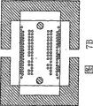
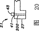
The invention provides a kind of chip carrier, this carrier can be on printed circuit board (PCB) with the array of three-dimensional pile up together or arrange two or more chips and the chips incorporate that will pile up in the circuit of circuit board.Fig. 1 is the perspective view of the preferred embodiment of chip carrier 21 of the present invention.Chip carrier 21 has roof panel 23 and two lateral braces 25 and 27.The IC chip that BGA liner 29A on platform 23 tops and the array of 29B are oriented to admit the method by the BGA array of pads to be connected.As hereinafter will discussing and illustrate, liner 29A and 29B are connected to the path that drops to platform 23, are connected by the lead that laterally leads to the path in the pillar 25 and 27 then.The top exposed portions 33 of each path in the pillar 25 and 27 can be seen on the top of the platform 23 on each pillar 25 and 27.As hereinafter will narrating and illustrate, each path in the pillar 25 and 27 is by pillar 25 and 27 and solder ball 37 can adhere to liner on it or the end of expose portion descends.Carrier 21 in an one preferred embodiment has the liner 41 that is used for admitting at the top of platform 23 decoupling capacitor 43.As hereinafter illustrating, decoupling capacitor is connected in the circuit by the path and the lead of suitable placement.In addition, being provided with of decoupling capacitor with the IC chip by chip strengthened service behaviour.The present invention provides the suitable decoupling of removing electric capacity like this.
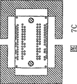
Fig. 2 provides the end view that is connected to circuit board 49 carriers 21 that have integrated circuit (IC) chip 51 and 52 of the present invention.IC chip 51 is connected to carrier 21 by the method for liner 29A and 29B (shown in Figure 1).IC chip 52 is connected to circuit board 49 by similar BGA array of pads group.Decoupling capacitor 43 is positioned on the angle of its platform 23 on the carrier 21.As mentioned above, the ball 61 of the BGA array of IC chip 51 is attached to that the array of liner 29A and 29B has the path that drops in its lower section in the platform 23 on the platform 23 on it, and path is connected to lead, and lead is connected to the path in pillar 25 and 27.Solder ball 37 is connected to the bottom of the path in pillar 25 and 27 circuit board 49 and is provided to being electrically connected at last of circuit board 49.IC chip 52 is connected to circuit board 49 by the solder ball 63 in the typical B GA array of pads that does not show on the circuit board 49.
In the embodiments of the invention of describing in Fig. 1 and 2, the liner of decoupling capacitor 43 has its oneself the conductive paths that pass through each pillar 25 and 27 declines that stop in solder ball 37.Decoupling capacitor is used for impedance Control, assist control return current and store charge.
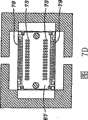
Fig. 3 provides circuit board 49, IC chip 52, the exploded view of carrier 21 and IC chip 51.Carrier 21 is connected to circuit board 49 by the method for BGA array of pads 65A and 65B.Circuit board 49 has a series of by the IC chipset of using and carrier 21 same or analogous carriers are arranged with cubical array.Circuit board 49 is typical printed circuit board (PCB), has the at all levels of the metallized of cambium layer laminated structure and prepreg thin slice, has the lead that does not show on it, lead connects various devices, in this case, these devices are IC chips 52, carrier 21 and IC chip 51.Circuit board 49 has connector 69 along its feather edge, and when circuit board 40 was inserted in the suitable socket of computer, connector was connected to the inner leads in the circuit board 49 remainder of system.Circuit board 49 is the typical circuit boards that can keep IC memory chip or similar chip.Fig. 3 only is used to be provided at the example of a kind of setting that wherein the present invention can be utilized.The present invention can be used to be located comprising of printed circuit board (PCB) other configurations of the extensive variation on the main motherboard of computer.
Path is made with the copper core in a preferred embodiment, and conductive channel also is made of copper.Like this, path 77D and 77A are the copper core, path 73A, and 73B, 73C and 73D are the copper core.Conductive channel 75A in a preferred embodiment, 75B and 75D are made of copper.Very natural, the every other path of carrier 21 and conductive channel all are made of copper identical form as shown in Figure 4.But also available any suitable electric conducting material.As shown in Figure 4 and can see from Fig. 1 and Fig. 3, the top of pillar 25 and 27 path has the end of the exposure that occurs on two top edge of the platform 23 at the top of pillar 25 and 27. Pillar 25 and 27 path needn't expose top such as the 79D of the 79A of path 77A and path 77D so that the function of carrier to be provided, and in fact, as a kind of alternative design, these tops can be covered by platform 23.But, construct these paths that have exposed top ends and much briefly mention or hereinafter with the feature of the uniqueness of detailed explanation for carrier 21 herein.The top of the exposure of pillar 25 and 27 path provides the contact point that exposes, and when the internal circuit of carrier, can test it by these contact points when IC chip 51 and 52 all is connected to printed circuit board (PCB).The top that exposes also provides the passage of heat radiation.In addition, the top of exposure provides at mutual top and has placed the similar carrier of one or more and carrier 21 to form the multiple cubical array that piles up of carrier and IC chip.In addition, with path 73A, 73B, 73C and 73D are that carrier has added extra heat-sinking capability from the bottom that the BGA liner on the platform 23 extends to platform 23.Another selection is to install and duration of test is that the top of the path in the pillar exposes, and after installation and test are finished with its covering.In addition, the fact is, in a preferred embodiment, carrier is made into the layering form similar with circuit board, and path also can be obstructed or by buried and be the path that communicates.
In a preferred embodiment of the invention, the path 73 of BGA liner 29A and 29B is directly placed under the liner of BGA array on the top of platform 23.This is the method for placing a kind of uniqueness of path, is a kind of common way because shown in the top that shows a BGA liner 81 and path 83 and Fig. 5 A of being connected conduction connection ring joint 84 path is setovered from liner.Is because it has the such fact of prostheses 86 of a hollow with liner 81 from a reason of liner 83 biasing.The prostheses 86 of hollow is the result of the following fact, because copper 82 or other electric conducting materials apply by electroplating technology, electroplating technology all stays the core of hollow usually.Like this, because the existence of hollow core 86 just can not be on path 83 the surface construction liner.Fig. 5 B is the profile of path 83 of taking from the V-V line of Fig. 5 A.Fig. 5 B shows the hollow core 86 in the path 85 that has copper liner 83.In a standard manufacturing processes, the path that the one or more levels by circuit board descend is by a little mechanical drill, and laser drilling tool or other device cuttings can reach similar result.In case path is drilled through just with the normally electric conducting material coating of copper.But liner can not deviate from spirit of the present invention from the path biasing shown in Fig. 5 A and 5B.But these technology have its defective as noted.
The invention provides the path of a solid core rather than the axle or the core 86 of hollow in a preferred embodiment.A kind of form is shown in Fig. 5 C.Fig. 5 C shown according to an alternative embodiment of the invention path 87 and the configuration of BGA liner 89.Path 88 among Fig. 5 C can be by forming the level manufacturing of copper 88 or other electric conducting materials 87, and the level of carrier is formed on wherein to form the passage of path 88.Should notice that the above-mentioned path that will descend directly is placed under the liner on the top of carrier has downwards reduced carrier and the required space of interlock circuit.It is to fill material non-conductive or conduction in the coated with conductive material is stayed hollow core in the path later on that another kind provided by the invention substitutes.Fig. 5 D has shown the hollow core 86 that material filled conductive or non-conductive 91 is later, and like this, along with filling hollow core 86 with electric conducting material 92 and 91, path 90 is filled into solid.Like this, liner 93 can be laid into the top of path 90.Very natural, the path in path in the carrier 21 and the pillar 25 and 27 can be with identical form manufacturing.
Provide as Fig. 6 of the schematic diagram of the downward cabling layer of carrier and can be how to be the schematic diagram of the example of the carrier configuration circuit made according to a preferred embodiment of the invention.The path 73 of the BGA array of carrier 21 is connected to specific passageways 77 in the pillar by conductive gasket 75.As reference, the profile of Fig. 4 is taken from I-I line shown in Figure 6.As seeing from Fig. 6 and other figure, the path 77 of preferred embodiment B-C post is aligned to staggered array has optimization with the edge along carrier 21 space.Also can see the connector 93 of decoupling capacitor liner among Fig. 6.The feature of a uniqueness of carrier of the present invention is the modification widely that the array pattern of the liner on table top can easily be configured to the IC Chip Packaging that can hold current manufacturing, uses or need not change fully the structure of carrier hardly.The internal circuit of carrier 21 can be configured to the modification widely of holding the IC chip and the suitable connection of IC chip to circuit board is provided.
As mentioned above, in a preferred embodiment, carrier of the present invention is made into the form identical with the printed circuit board (PCB) of standard.In a preferred embodiment, carrier can have two to four or many levels more.Fig. 7 A, 7B, 7C and 7D provide the schematic diagram at all levels of the top platform that can constitute carrier.Fig. 7 A has described to comprise the bottom of conductive channel 75.Fig. 7 B has described internal grounded layers, and Fig. 7 C has described internal power plane and Fig. 7 D has described to have the top layer that the IC chip is arranged the liner that is connected thereto.Fig. 7 B and 7C are the negative views of the level of describing, and Fig. 7 A and 7D are front view.In addition, in the preferred embodiments of the present invention of Fig. 7 D, electrical isolation around the surface 67 of the exposed ends 79 of path and the liner 73 of BGA array and carrier.In a preferred embodiment, surf zone 73 is the electric conducting materials such as copper.In a preferred embodiment, one surround each liner 73 but and the zonule 67 of liner 73 electrical isolation provide ground area to be used for purposes such as test adjacent to the top of each liner 73 and path 79.Well-known technically, Fig. 7 A, the level that 7B, 7C and 7D describe are by all levels is bonded together but the prepreg layer of its electrical isolation is separated.
It is the diagrammatic side view that can constitute the order at all levels that has the carrier at all levels that Fig. 7 A describes to 7D.In Fig. 8 A, routing layer 101 is bottoms.Next is a prepreg layer 102, and ground plane 103 thereon.The core layer 104 that is positioned at carrier center is adjacent with ground plane 103.Then, behind the bus plane 105 prepreg layer 106, be top routing layer 107 at last.
Make carrier 21 a lot of significantly advantages are provided with being attached to printed circuit board (PCB) identical materials on it with carrier.These advantages have, and carrier 21 will be coordinated mutually with other elements in the circuit of the printed circuit board (PCB) that will be connected thereto.The electric characteristic of carrier in design process, chip carrier 21 of the present invention is attached in the circuit of circuit board and can not cause tangible problem, because will be understood well and coordinate mutually with other elements in the circuit.
In a preferred embodiment of the invention, pillar 110 and 111 is also made with the material of prepreg laminated-type.Pillar will be based upon in laminated material at all levels.Also can use additive method such as injection molding process.
Fig. 8 B provides another profile of the part of the pillar 112 of carrier of the present invention and platform 113.Discussed abovely at all levelsly can begin to see that top layer 114 has the figure of BGA liner from top layer 114, be first prepreg layer 115 in its lower section.Industrial well-known prepreg layer be insulation is provided between the conductive layer and provide form circuit board or under this situation for forming the necessary rigidity of carrier and the laminated material of support.In first prepreg layer is for 115 times power plane layer 116, at its downside one second prepreg layer 117 is arranged.In second prepreg layer is for 117 times ground plane 118, is the 3rd prepreg layer 119 in its lower section.Last is downward cabling layers 120 in the bottom of platform 113.At all levels 114,115,116,117,118,119 and 120 have formed the platform 113 in the preferred embodiment like this.For forming pillar 112, these levels continue to form the 4th prepreg layer 121 again, and another intermediate layer 122, the five prepreg layer 123 and end at bottom 124 are liners 125 of path 77 in the bottom of bottom 124.Aforesaid path 77 descends by the top edge of platform 113, ends at liner 125 by pillar 112, and solder ball 126 is attached to liner 125, is used for carrier being connected to circuit board or another carrier as what hereinafter will narrate.In a preferred embodiment of the invention, the top 79 of path 77 ends at liner 127 in the pillar 112.
A path 77A who has only shown pillar 112 in the cross section of Fig. 8 B is because drop to strut via in the pillar by platform edges and can edge-to-edge ground aim at and do not deviate from principle of the present invention to save the space for staggered along the path 77A at the edge of carrier in a preferred embodiment.In this specification as above-mentioned discussion at the path 73 that shows on the profile and in other figure, describe the liner 128 of the BGA array of pads of IC Chip Packaging is connected to lead 75, lead 75 is connected to path 77A more successively.Conductive channel 75 is made by copper cash as mentioned above.But, also available any other suitable electric conducting material.As in this manual other places pointing out, in a preferred embodiment, the solid copper core of path 77 and 73 for during the manufacturing process of carrier, forming.Therefore top and bottom that the electrically conductive core of formation path terminates in each pillar of carrier also provide the passage that dispels the heat.Point out as other parts of this specification, these passages that form path therein also can by boring in the level of carrier and in the hole copper facing or other suitable electric conducting materials make.
Make carrier with multi-level form as mentioned above many advantages are provided, it accomplishes the impedance matching of carrier and circuit board, carrier is adapted to and the IC chip of any standard is worked together and needn't be revised chip etc.In addition, laminating technology step by step, degree of depth cabling or other building methods can be used for making the path and the conductive channel of carrier.Though the preferred embodiment that is disclosed is made with the form identical with multi-level circuit board, also can have the various carriers that do not need that multi-level application is arranged.This is used for various application carrier and can makes by injection molding process or similar technology.Even by the carrier that injection molding process is made, its structure also still can be revised.
As mentioned above, semi-conductor industry has generally adopted the connector of BGA type for integrated circuit (IC) chip.Improvement and other reason on the systematic function that connects with the connector of BGA type have been stipulated the transformation that connects from the lead to BGA.But is such fact with lead with the advantage that integrated circuit (IC) chip is connected to circuit board or other retainers, as fruit chip or related device generation problem later on is installed, can easily test element, need not from circuit, to take off element by lead.But for the chip that connects by BGA,, question unit must be taken off from the circuit that printed circuit board (PCB) or other devices adhere to, because be what to touch less than the ball of linkage unit when main unit is connected to circuit for test element.Can change its operating characteristic fully but chip or other unit taken off from circuit of problem takes place for it, if therefore can not determine that the actual cause of initial problem will make work become very difficult.Can have many methods to set, but carry out the required time of this work and make great efforts to make it become very expensive, and efficient is not high, also technologic mistake can take place near the work of chip or device generation problem.
A tangible advantage of the present invention provided a kind of just can be when IC chip and carrier all also are connected on the circuit of printed circuit board (PCB) to its means of testing and method.As mentioned above, realize on the top of the exposure that this can be by the path 77 in the pillar that does not show among Fig. 9.Fig. 9 provides one jiao the perspective view that is connected to the carrier 130 of circuit board 131 of the present invention.The IC chip 132 that is connected to carrier 130 by the BGA array is connected to the top of carrier.Another IC chip is connected on the circuit board 131 under the carrier 130.The part of the array on the top 134 of the exposure of path in the pillar 135 is exposed by the top along carrier 130.Be given the position of exposure on the top 79 of path, can be placed in against the top of living to expose and carry out various tests to determine the reason of any problem that circuit and device take place from the sensing point 136 and 137 of one or more test devices.This to all also being connected the carrier of the present invention on the printed circuit board (PCB) and being connected thereto and being positioned at IC chip it under or ability that other BGA devices are tested not only makes result of the test very accurate, and make test efficiency high and operate easily.The test that utilizes the top 79 of exposure of the path of pillar to carry out can become the part of the standard quality control test of carrying out during manufacturing process automatically.This can carry out with several different methods, comprises using having the grab type testing equipment of visiting a little more, and these spies are named a person for a particular job in the array 134 of exposure at the top that is connected to the path in the pillar as required at any time.
With reference to figure 8C and 9, peripheral region 67 electrical isolation of the top 79 of the exposure of upwardly extending path and table top.The liner of path and BGA array 69 also passes through peripheral region 67 electrical isolation at the top of material 80 and platform 23.In a preferred embodiment, many top area 67 covering copper layers.This copper layer is used as fin.The part of top insulating barrier 68 cover layers 67.This also provides ground connection contact point easily for test unit 71.For example the probe 136 among Fig. 9 and Fig. 8 C or one of 137 can be placed in against the top 79 of living a path, and another can be placed in against the zone 67 and form ground connection.Underproof circuit and relevant IC chip on carrier of the present invention has at a high speed and high complexity, and point-device testing equipment also needs to test.Adjacent to the test contact point that will carry out ground connection is set thereon and will makes test easily, because the spy point of testing equipment 136 and 137 placement adjacent to each other in the test prod 71 of being everlasting, shown in Fig. 8 C.
The structure of carrier of the present invention provides additional substituting for the adjacent ground connection that is used for the circuit test.One or more tops of the path that exposes in the pillar are the connection of a ground connection with most probable.Like this, in carrying out a test, the path of this exposure can be used as test for ground, needn't provide a special adjacent earthing position for the testing site.
Another advantage that the path of exposure top 134 (Fig. 9) is provided that is relevant to mentioned above is the ability of piling up multichip carrier and IC chip in the cubical array of an amplification.Figure 10 is the exploded view how chip and carrier pile up.In Figure 10, a BGA device 139 is attached on the circuit board 140 by standard BGA array.The array of the BGA liner 142 of any side of carrier 141 by being positioned at BGA device 139 is connected to circuit board successively.BGA device 145 usefulness BGA array of pads 147 are connected to carrier 141 tops successively.Carrier 149 is attached to carrier 141 by the method for the array 150 on the top of the exposure of the path in the pillar of carrier 141 successively.At last, BGA device 153 is attached to carrier 149 by the method for the array of the BGA liner 154 at carrier 149 tops.Two stackable carriers though only draw among Figure 10, multiple carrier can pile up mutually together with the BGA device that adheres to.Figure 11 provides the end-view of two stacked carriers 161 that form the cubical array that amplifies on the circuit board 167 and the BGA device 163 that adheres to.Figure 12 provides the array of carriers of piling up and the end view of BGA device.Among Figure 12, the BGA device below each carrier 161 can not be seen owing to the position of the pillar 169 of each carrier 161.
The another kind of form of carrier 201 of the present invention is described in Figure 13.Carrier 201 is attached to printed circuit board (PCB) 205.IC chip 210 is attached to carrier 201 in the above described manner.But, IC chip 211 be attached to carrier 201 platform 215 vocabulary face 213 rather than be attached to circuit board 205 below the carrier.The IC die attach is arrived the bottom of carrier 201 with the BGA array of pads of locating along the basal surface 213 of carrier 201.This array is identical with above-mentioned array.Can carry out any amount of different circuit connects successively the IC chip to be connected in the circuit by carrier 201 and goes.In fact, this quantity is very many, is difficult to describe.This is a tangible advantage of the present invention, carrier can with the IC chip of suitable BGA array of pads and circuit configuration together with the in fact any kind of in the top of the platform 215 that keeps being fitted to carrier 201 or the space on the bottom.
Figure 14 provides can be by the view of a kind of potential circuit arrangement of the liner that uses together with the memory IC chip, and this kind arrangement provided the redundancy of the circuit that has carrier 201 (Figure 13).In Figure 14, the roof liner pad 220 of solid outline is positioned at the top of the platform of carrier.Each liner 220 at the top is connected to a path 225 by solid line 223.As mentioned above, path drops to the bottom of platform by platform, locates each path at this and is connected to the line 227 that shows with the outline line form.Every line 227 is connected to the liner 229 that shows with the outline line form in the bottom of carrier successively.As seen in FIG., each liner 220 and the liner 229 in the bottom at the top all are connected to same path.But, setover from liner at the top at the liner of bottom.This is because such fact, the example of usefulness is a memory chip herein, this memory chip will have identical arrangement, when being placed in any side of carrier, the identical liner that can link together from the memory IC chip that uses in this example will be setovered mutually, and the bottom of each chip faces one another at that time.Figure 15 provides the profile of taking from the II-II line of the platform of Figure 14 demonstration.As seen in FIG., the liner on the 220A of top is connected to path 225A by line 223A.Path 225A descends by platform 230.Path 225A is connected to line 227A.Line 227A is connected to liner 229A successively.
An advantage of the carrier format that Figure 13 describes is, printed circuit board (PCB) can be made the configuration of standard and carrier 201 that Figure 13 describes is worked together.Like this, must be had only carrier 201 with the element of processing IC chip by line.
Figure 16 provides an example of the printed circuit board (PCB) 251 that has carrier 253.In Figure 16, the IC chip that is positioned at carrier 253 tops is not also added.Can see like this, the BGA liner 255 that is used for adhering to the IC chip is attached to the top of each carrier 253.Can also see by platform and below the liner 257 at top of the path that descends of pillar.In Figure 17, the IC chip has been attached to the top of carrier 253.BGA liner 255 is no longer in sight, because chip 259 is with its covering now.But the liner 257 at the top of the path that descends at each platform by carrier and pillar is clear that and can be because of above touching with other purposes with the test of description.
Very natural, BGA array of pads 255 on each carrier can be with any amount of distinct methods configuration, thereby if a kind of IC chip is in array that Figure 16 describes or any other configuration of the array of the matrix type described such as Figure 18 in, just can accept the BGA array of pads of the presumable any kind of this IC chip.Because carrier can easily carry out line with the diverse ways of extensive variation, this carrier can be designed to work together with the IC Chip Packaging of any standard and need not revise the encapsulation of IC chip.Carrier of the present invention is a kind of module device really.In fact, carrier provide a kind of be used for the IC die attach to the standard of circuit board but sell alignment methods flexibly.
Also have, as mentioned above, the present invention is BGA, and the IC Chip Packaging of CSP and a lot of other types provides a kind of three-dimensional devices of uniqueness.The present invention also provides suitable capacitor decoupling.In addition, the present invention also provides and surveys or the testing site, for signal sampling provides array 257 (being 79) in some figure, for partial assembled provides testing site etc.Also have, the present invention also provides the tight close earth point adjacent to the sensing point of carrier top, no matter whether the IC chip is placed in the top of carrier, these earth points can obtain.
Another one advantage of the present invention is that it can be used in the logical manufacturing process of density current of three-dimensional single side face.The ground floor of IC chip can be placed on the circuit board, then carrier placed as illustrated in fig. 16 this chip above, the second last group IC chip can place the top of carrier as illustrated in fig. 17.In case this configuration is finished, the entire circuit plate and be placed in the part at its top only must be through a substance flow-through process to finish manufacturing.Can be with whole IC chips and carrier being installed such as picking up of standard with the manufacturing machine of the standard of placement device.Carrier as mentioned above, can use the IC Chip Packaging of the unmodified of standard in several places, because can also can comprise the chip that has lead, and have the BGA liner, flip-chip, the chip of CSP etc. by staggered to accept the IC chip of any standard.In addition, carrier can be placed on the conveyer belt that is used for manufacturing process or transmit with the dish of the JEDEC type of standard.
Figure 18 provides the schematic diagram of the liner that the top of carrier 30 as one kind 1 in a preferred embodiment occurs.As shown in FIG., a matrix that is used to connect the liner 303 of IC chip is arranged.As shown in FIG., there is one the eight row five-element's solid pads matrix to be used to admit the IC chip.All can be used to connect suitable IC chip as well-known technically, all liner or its any combination.In addition, as seeing at each face, the array of a strut pads 305A and 305B appears.As noted above, these liners are connected to IC liner matrix 303 with suitable figure.In addition, be useful on the liner of the suitable device of capacitor or other types at each angle 307.As shown in FIG., each pin all has a suitable sign, such as Vdd, or DQ2, or NC etc.For example, in configuration shown in Figure 180, liner DQ0 is connected to strut via pad 310.As shown in the figure, strut pads is denoted as the various pins of traditional form.By the table of reference Figure 19, the connection between the liner on the matrix of liner 303 and each pillar is indicated by the pin conversion table.This only is the example that possible liner connects, and this example can be made the dissimilar chip that is used to have bigger variation, has the various liner configuration that can be connected with carrier 30 as one kind 1.
The schematic diagram that Figure 20 provides decoupling capacitor 43 how to be electrically connected as described above.Capacitor 43 is positioned on the liner (Fig. 1) of two separation, and each liner all is connected to the path of separation, and one is connected to ground connection, and another is connected to power supply.In Figure 20, decoupling capacitor 43 places on the liner 41.Liner 41 is connected to path 300, and path 300 is by pillar 27 declines of carrier 21, a jiao of can see carrier 21 in Figure 20.Path 300 is connected to not on the suitable liner on the circuit board that shows.Very natural, described two each liners of liner of decoupling capacitor connection among Fig. 1 and be connected to the tie point of power supply or ground connection, thereby become the part of the electronic structure of circuit by the path that separates.
The present invention in another kind of modification can be used for decoupling capacitor 303 is positioned at various position on the carrier 30 as one kind 1 as shown in figure 21.Decoupling capacitor 303 is to the realization that can in all sorts of ways that is electrically connected of system.How the liner 305 and 306 that a kind of modification shown in Figure 21 A, the profile of the X-X line of taking from Figure 20 of carrier 30 as one kind 1 have been described decoupling capacitor 303 places is connected to the inside ground connection 309 and the power plane 310 of the structure that constitutes carrier 30 as one kind 1 as mentioned above by path.Internal power plane 310 is connected at least one path 311 in the pillar, and internal power plane 309 is connected to a path 312 in the pillar.Very natural, all tie points that are connected to internal power plane 310 are connected to the tie point electrical isolation of internal power plane 309 with all.In the another kind of modification that Figure 21 B describes, be connected to lead 317 and 318 from the liner 305 and 306 paths 314 and 315 that descend at decoupling capacitor 303 places, lead 317 and 318 is directly connected to the path 320 and 321 in the pillar 325 that power supply and ground connection tie point are provided again successively.
Figure 22 provides a kind of form of the distributing on the wiring substrate layer 401 of carrier of the present invention.In the distributing of Figure 22, can see a part that is connected to the path 403 that the liner at the top of the platform on it descends from the IC chip.In addition, the various piece of the path in the pillar 405 occurs along the edge of carrier.In addition, the trend of conductive channel 407 is between passage portion 403 and the passage portion 405.One of important operating aspect of any computer system all provides the sequential of appropriate signals motion.May can often produce the operation problem that the speed by the current operation of computer provides at one millisecond even the signal that in a picosecond, disappears.In addition, trend is to improve the number of times of clock signal of operation and the speed of computer, and like this, sequential will become in the future even more occupy conclusive status.An advantage of the invention is that it can arrange the chip of memory or other types with the form of three-dimensional, such form can reduce the length of connecting line.This is normally conclusive and obviously help the raising of the speed of service in computer technology.In fact, the quick clock cycle period in computer operating system, signal must arrive specific end points with the coordinated mode motion and in clock cycle period.If signal must be all equally long for each signal with the lead of coordinated mode motion thereon, just can obviously be reduced from the effect of the problem of coordinating the signal generation.Another advantage of carrier of the present invention is if several signal must move on adjacent lead at the same time, by the conductor length on the staggered via location matches substrate, can make lead that accurate identical length is arranged.Shown in the distributing that Figure 22 describes, some have equal lengths to the lead 407 that moves towards between the via set 405 in via set 403 in many connections.For example, indicate all leads of 407 among Figure 22 identical length is all arranged.In addition, at the opposite side of the distributing of Figure 22, the lead of trend has identical length 410 between passage portion 403 and passage portion 405.Like this, if be placed in the accurate parallel transmission that chip on the carrier needs multiple signal simultaneously, on carrier, provide the transmission line of equal length to reduce the possible loss of the harmony of parallel signal transmission significantly.
Though the present invention has been carried out concrete demonstration and narration with reference to its preferred embodiment, skilled technically personnel will be appreciated that and can make various variations in form and details and not deviate from the spirit and scope of the present invention the present invention.
Claims (52)
1. carrier that is used on circuit board arranging integrated circuit (IC) chip with cubical array, described carrier comprises:
A) platform that has top surface and basal surface;
B) at first pillar of first side of described platform with at second pillar of second side of described platform, described pillar is that described platform provides support, thereby produces a space under the basal surface of described platform;
C) described platform has a figure that connects liner to be used for connecting on the top surface of figure of liner at its top surface to admit at least one integrated circuit (IC) chip, the bottom side of each liner of the described figure of liner is connected to the path that drops to the lower floor of described platform by described platform, and wherein said path is connected to the conductive channel that extends towards described first or second pillar;
D) described first and second pillars have by each pillar from the bottom of described pillar to the upwardly extending strut via in the top of described pillar, wherein each described strut via is connected to a specific conductive channel in the described platform, and this specific conductive channel is connected to a specific path that descends from the liner of the liner of the figure of connection liner;
E) the described upwardly extending strut via in wherein said first pillar extends to the top edge of described first side of described platform, thereby be exposed to the top surface of the described upwardly extending strut via on the described top surface of described platform, described upwardly extending strut via in described second pillar extends up to the top edge of described second side of described platform, thereby is exposed to the top edge of the described upwardly extending strut via on the described top surface of described platform;
F) wherein said carrier forms a modular unit, this modular unit can be accepted at least one integrated circuit (IC) chip on the top surface of the described platform on the described figure that connects liner, and this chip is connected to printed circuit board (PCB), wherein said carrier is attached to this printed circuit board (PCB), and provides one to be used for being attached to major general's second integrated circuit (IC) chip described carrier and to be attached to space on the circuit board on it in the space under the basal surface of described carrier; With
G) wherein said path is by forming with electric conducting material plating hole.
2. carrier as claimed in claim 1 is characterized in that described upwardly extending path has the core of an electric conducting material.
3. carrier as claimed in claim 1, it is characterized in that, the described figure of the described connection liner of described platform can change to form multiple different array pattern, thereby make described carrier be held various integrated circuit (IC) chip widely with different array patterns, wherein, between described path and described connection liner, and the described conductive channel between described path and described pillar can be configured as with multiple different configuration the described connection liner figure on the described platform is connected to circuit board.
4. carrier as claimed in claim 1 is characterized in that integrated circuit (IC) chip can be connected to array of pads by lead.
5. carrier as claimed in claim 1, it is characterized in that, thereby filled the space of removing described hollow with the material of selecting in advance with the space of staying the hollow in the described hole behind the described hole of electric conducting material plating, and allow to connect the top that liner is positioned at described path, thereby must avoid described liner to setover from described path.
6. carrier as claimed in claim 5 is characterized in that, the described material of selecting in advance is a kind of non-conducting material.
7. carrier as claimed in claim 5 is characterized in that, the described material of selecting in advance is a kind of electric conducting material.
8. carrier as claimed in claim 4, wherein:
A) top of the described top exposure of the described upwardly extending path in described first pillar is positioned at the top circumference edge of described first side of the described platform that the first predetermined figure is arranged, the top that the described top of the described upwardly extending path in described second pillar exposes is positioned at the top circumference edge of described second side of the described platform that the second predetermined figure is arranged, and
B) the area yardstick of the described top surface of described platform is, the described top surface of described platform can hold at least one integrated circuit (IC) chip that is connected by the figure that connects liner at described top surface, stays the described second predetermined figure on the top that the top of the described first predetermined figure on the top that the top without the described upwardly extending path that covers and can touch exposes and described upwardly extending path exposes simultaneously.
9. carrier as claimed in claim 1 is characterized in that, described first and second pillars are pillars of the described platform of a plurality of supports.
10. carrier as claimed in claim 1 is characterized in that described liner is directly over described path.
11. carrier as claimed in claim 1 is characterized in that, described liner departs from described path.
12. carrier as claimed in claim 1 is characterized in that, employed connection liner is selected from the set of BGA liner or Chip scale liner.
13. carrier as claimed in claim 1 is characterized in that, described second integrated circuit (IC) chip is positioned on the bottom surface on described surface of described platform, and is connected to circuit board by through hole and the lead in described first and second pillars and described platform.
14. carrier as claimed in claim 1 is characterized in that, further comprises the liner that is used at least one decoupling capacitor is connected electrically to described carrier.
15. carrier as claimed in claim 14 is characterized in that, the described liner that wherein is used for described at least one decoupling capacitor is connected to the bus plane or the ground plane of described carrier, thereby described at least one decoupling capacitor is connected in the circuit.
16. carrier as claimed in claim 14, it is characterized in that, the described liner that is used for described at least one decoupling capacitor is connected to the path of pillar, when described carrier is attached to circuit board, described path is connected to power supply and the ground connection tie point on the described circuit board, thereby described at least one decoupling capacitor is connected in the circuit.
17. carrier as claimed in claim 16 is characterized in that, described liner is positioned at the top of described pillar.
18. carrier as claimed in claim 1 is characterized in that, wherein said carrier is manufactured into and is the multi-layer sheet similar in appearance to the form of preferred circuit plate.
19. carrier as claimed in claim 1 is characterized in that, described carrier is by the injection molding process manufacturing.
20. carrier as claimed in claim 1 is characterized in that, described path is by the technology manufacturing of selecting from the set of step layer platen press or degree of depth wiring method.
21. carrier as claimed in claim 1 is characterized in that, when described carrier was attached to circuit board, described second integrated circuit (IC) chip was directly connected to the circuit under the described bottom surface of the described platform of described carrier.
22. a carrier that is used for arranging with cubical array integrated circuit (IC) chip on circuit board, described carrier comprises:
A) platform that has top surface and basal surface;
B) at first pillar of first side of described platform with at second pillar of second side of described platform, described pillar is that described platform provides support, thereby produces a space under the basal surface of described platform;
C) described platform has a figure that connects liner to be used for connecting on the top surface of figure of liner at its top surface to admit at least one integrated circuit (IC) chip, the bottom side of each liner of the described figure of liner is connected to the path that drops to the lower floor of described platform by described platform, and wherein said path is connected to the conductive channel that extends towards described first or second pillar;
D) described first and second pillars have by each pillar from the bottom of described pillar to the upwardly extending strut via in the top of described pillar, wherein each described strut via is connected to a specific conductive channel in the described platform, and this specific conductive channel is connected to a specific path that descends from the liner of the liner of the figure of connection liner;
E) wherein said carrier forms a modular unit, this modular unit can be accepted at least one integrated circuit (IC) chip on the top surface of the described platform on the described figure that connects liner, and this chip is connected to printed circuit board (PCB), wherein said carrier is attached to this printed circuit board (PCB), and provides one to be used for being attached to major general's second integrated circuit (IC) chip described carrier and to be attached to space on the circuit board on it in the space under the basal surface of described carrier;
F) the described upwardly extending strut via in wherein said first pillar extends to the top edge of described first side of described platform, thereby be exposed to the top surface of the described upwardly extending path on the described top surface of described platform, described upwardly extending strut via in described second pillar extends up to the top edge of described second side of described platform, thereby is exposed to the top edge of the described upwardly extending path on the described top surface of described platform; And
G) wherein said strut via is by forming with electric conducting material plating hole.
23. carrier as claimed in claim 22 is characterized in that, described upwardly extending path is suitable for providing heat dissipation.
24. carrier as claimed in claim 22 is characterized in that:
A) top of the described top exposure of the described upwardly extending path in described first pillar is positioned at the top circumference edge of described first side of the described platform that the first predetermined figure is arranged, the top that the described top of the described upwardly extending path in described second pillar exposes is positioned at the top circumference edge of described second side of the described platform that the second predetermined figure is arranged
B) the area yardstick of the described top surface of described platform is, the described top surface of described platform can hold at least one integrated circuit (IC) chip that is connected by the figure that connects liner at described top surface, stays the described second predetermined figure on the top that the top of the described first predetermined figure on the top that the top without the described upwardly extending path that covers and can touch exposes and described upwardly extending path exposes simultaneously;
C) the predetermined figure of the mirror images of the promising described first predetermined figure in the bottom of the described bottom-exposed of the described path of wherein said first pillar, the predetermined figure of the mirror images of the promising described second predetermined figure in the bottom of the described bottom-exposed of the described path of described second pillar; With
D) its described first carrier that neutralizes at the yardstick of described first and second mirror images of the described first and second predetermined figures and the first and second predetermined figures and in arranging on all four second carrier can be stacked on described first carrier, the top that the described top of the described path of described first carrier exposes contacts with the bottom of the described bottom-exposed of described second carrier is electric.
25. carrier as claimed in claim 24, it is characterized in that, at least one integrated circuit (IC) chip can be connected in the space under the basal surface of the above first carrier of described circuit board, at least one integrated circuit (IC) chip can be connected on the described top surface of the described platform on described first carrier, at least one integrated circuit (IC) chip can be connected on the described top surface of described platform of described second carrier, and all described integrated circuit (IC) chip can be electrically connected in the circuit of described circuit board.
26. carrier as claimed in claim 24 is characterized in that, a plurality of identical carriers can be placed on another to form the cubical array of the carrier that is electrically connected mutually by one.
27. carrier as claimed in claim 25, it is characterized in that, the described figure that connects liner on the described platform of two carriers can change so that described carrier holds various widely integrated circuit (IC) chip with different array patterns, and wherein the described conductive channel between the described path of the described path of the described liner of described connection liner and described pillar can be configured as with multiple different configuration the described figure of the connection liner on the described platform is connected to circuit board.
28. carrier as claimed in claim 26, it is characterized in that, the described figure of the connection array of pads on the described platform of described a plurality of carriers can change so that described carrier holds various widely integrated circuit (IC) chip array of pads figures, and wherein the described conductive channel between the described path of the described path of the described liner of described connection array of pads and described pillar can be configured as with multiple different configuration the described liner on the described platform is connected to described path in described first and second pillars.
29. carrier as claimed in claim 24, it is characterized in that, when described first and second carriers and any integrated circuit (IC) chip of adhering to are connected to circuit board, be provided for testing the contact point of described carrier and described integrated circuit (IC) chip on the top of the described exposure of upwardly extending path described in the described pillar of described second carrier.
30. carrier as claimed in claim 25, it is characterized in that, when described first and second carriers and any integrated circuit (IC) chip of adhering to are connected to circuit, be provided for testing the contact point of described carrier and described integrated circuit (IC) chip on the top of the described exposure of upwardly extending path described in the described pillar of described second carrier.
31. carrier as claimed in claim 26, it is characterized in that, when described a plurality of carriers that pile up and any integrated circuit (IC) chip of adhering to are connected to circuit, be provided for testing the contact point of described carrier and described integrated circuit (IC) chip on the top of the described exposure of upwardly extending path described in the described pillar of roof carrier.
32. carrier as claimed in claim 22 is characterized in that, described liner be positioned at described path directly over.
33. carrier as claimed in claim 22 is characterized in that, described liner departs from described path.
34. carrier as claimed in claim 22, it is characterized in that the top that the described top of the path in described pillar exposes provides carries out single analysis site of analyzing to described carrier when this carrier is connected to the circuit board that has at least one integrated circuit (IC) chip that is connected to described carrier.
35. carrier as claimed in claim 22, it is characterized in that, the top that the described top of the described path in described pillar exposes is used to test or signal analysis, and wherein the top that exposes adjacent to the described top of described path of at least one earth point is with the analysis or the test of convenient signal.
36. carrier as claimed in claim 35, it is characterized in that, select in the set of the specific ground area on the top that described at least one earth point exposes from the described top adjacent to the described path the described pillar, or the top that the described top of at least one described path exposes is an earth point.
37. carrier as claimed in claim 35 is characterized in that, wherein said signal analysis or test are undertaken by probe points.
38. carrier as claimed in claim 22 is characterized in that, when described carrier was attached to circuit board, the top of the exposure of described strut via provided test point to connect to test described carrier.
39. carrier as claimed in claim 22, it is characterized in that, thereby wherein be filled in advance the space that the material selected is removed described hollow, be positioned at the top of described path and must avoid described liner to setover from described path with connecting liner with the space of staying the hollow in the described hole behind the described hole of electric conducting material plating.
40. carrier as claimed in claim 39 is characterized in that, the described material of selecting in advance is an electrically non-conductive material.
41. carrier as claimed in claim 39 is characterized in that, the described material of selecting in advance is an electric conducting material.
42. carrier as claimed in claim 39, wherein:
A) top of the described top exposure of the described upwardly extending path in described first pillar is positioned at the top circumference edge of described first side of the described platform with first predetermined figure, the top that the described top of the described upwardly extending path in described second pillar exposes is positioned at the top circumference edge of described second side of the described platform with second predetermined figure, and
B) the area yardstick of the described top surface of described platform is, the described top surface of described platform can hold at least one integrated circuit (IC) chip that is connected by the figure that connects liner at described top surface, stays the described second predetermined figure on the top that the top of the described first predetermined figure on the top that the top without the described upwardly extending path that covers and can touch exposes and described upwardly extending path exposes simultaneously;
43. a carrier that is used for arranging with cubical array integrated circuit (IC) chip on circuit board, described carrier comprises:
A) platform that has top surface and basal surface;
B) at first pillar of first side of described platform with at second pillar of second side of described platform, described pillar is that described platform provides support, thereby produces a space under the basal surface of described platform;
C) described platform has a figure that connects liner to be used for connecting on the top surface of figure of liner at its top surface to admit at least one integrated circuit (IC) chip, the bottom side of each liner of the described figure of liner is connected to the path that drops to the lower floor of described platform by described platform, and wherein said path is connected to the conductive channel that extends towards described first or second pillar;
D) described first and second pillars have by each pillar from the bottom of described pillar to the upwardly extending strut via in the top of described pillar, wherein each described strut via is connected to a specific conductive channel in the described platform, and this specific conductive channel is connected to a specific path that descends from the liner of the liner of the figure of connection liner;
E) the described upwardly extending strut via in wherein said first pillar extends to the top edge of described first side of described platform, thereby be exposed to the top surface of the described upwardly extending strut via on the described top surface of described platform, described upwardly extending strut via in described second pillar extends up to the top edge of described second side of described platform, thereby is exposed to the top edge of the described upwardly extending strut via on the described top surface of described platform;
F) wherein said carrier forms a modular unit, this modular unit can be accepted at least one integrated circuit (IC) chip on the top surface of the described platform on the described figure that connects liner, and this chip is connected to printed circuit board (PCB), wherein said carrier is attached to this printed circuit board (PCB), and provides one to be used for being attached to major general's second integrated circuit (IC) chip described carrier and to be attached to space on the circuit board on it in the space under the basal surface of described carrier;
G) further comprise the liner that is used to be electrically connected at least one decoupling capacitor to described carrier;
H) the described liner that wherein is used for described at least one decoupling capacitor is connected to the path of pillar, when described carrier is attached to circuit board, described path is connected to power supply and the ground connection tie point on the described circuit board, thereby described at least one decoupling capacitor is connected in the circuit; And
I) the described liner that wherein is used at least one decoupling capacitor is connected to the described path of described pillar by alternate path, and this alternate path is connected to conductive channel, and this conductive channel is connected to the described path in the described pillar successively.
44. a method of arranging integrated circuit (IC) chip on circuit board with cubical array, described method comprises the following steps:
A) provide a platform that is used to admit first integrated circuit (IC) chip;
B) thus provide at least one supporting strut to support described platform and to form a carrier;
C) when carrier is connected to circuit board, described chip is connected electrically to circuit board by this platform and pillar;
D) form at least one pillar and platform with the configuration that a space is arranged under the bottom of platform, like this, a space that is used for second integrated circuit (IC) chip is connected to circuit board is arranged under platform when carrier is attached to circuit board;
E) be attached to the test contact that can be touched when circuit board and integrated circuit (IC) chip are connected to the top of platform providing on the carrier when carrier, the top that this step is included at least one pillar provides the top of the exposure of path;
F) wherein integrated circuit (IC) chip being connected electrically to the platform carrier, to be attached to the step of the plate on it as follows: provide connection liner from the top of platform to extend downwardly into the conductive path of the articulamentum the carrier; Path is connected to conductor wire in the articulamentum; Determine to lead to the trend of the conductor wire of at least one pillar; Provide conductive path will having in the pillar that the conductor wire of the figure of selection is connected thereto in advance of at least one; Make conductive path at least one the pillar drop to the bottom of the pillar of at least one from the place that this path is connected to conductor wire; Stop conductive path at least one the bottom of pillar that is used for carrier is connected to the connection liner place of circuit board;
G) wherein provide the path that descends from platform and the step of the path at least one pillar to comprise: in platform or pillar, to provide the hole; Depositing conductive material in the hole; With
H) comprise further in the hollow space left after other packing material is deposited to depositing conductive material and finishes to the step in the hole and removing.
45. method as claimed in claim 44 is characterized in that, the step of described other packing material of deposit comprises the non-conductive packing material of deposit.
46. method as claimed in claim 44 is characterized in that, the step of described other packing material of deposit comprises the deposit conductive filling material.
47. a carrier that is used for arranging with cubical array integrated circuit (IC) chip on circuit board, described carrier comprises:
A) be used to provide the device of the platform of admitting first integrated circuit (IC) chip;
B) thus be used to support the device that described platform forms a carrier, described carrier has a space under carrier, thereby provides the space for second integrated circuit (IC) chip is connected to circuit board when described carrier is attached to circuit board;
C) when described carrier is connected to circuit board, first integrated circuit (IC) chip that the device by the described platform of described support will be connected to the top of described carrier is connected electrically to the device of circuit board;
D) wherein, first integrated circuit (IC) chip that the device by the described platform of described support will be connected to the top of described carrier when described carrier the is connected to circuit board device that is connected electrically to circuit board comprises:
I) extend downwardly into the conductive path of the connection level the described carrier from a plurality of connection liners on the top of platform;
Ii) in described articulamentum, be connected to from connecting the liner lead of the conductive path of extension downwards;
Iii) wherein supporting arrangement is at least one pillar and the lead that is connected to described at least one pillar;
The conductive path that iv) in the pillar of at least one, has in advance the conductor wire of the figure of selecting be connected thereto;
V) wherein the conductive path in the pillar of at least one drops to the bottom of the pillar of at least one from the place that this path is connected to conductor wire; And terminate at least one the bottom of pillar that is used for carrier is connected to the connection liner place of circuit board;
E) wherein the conductive path in the pillar of platform and at least one forms by the hole that electric conducting material is deposited on wherein;
F) its mesopore comprises the packing material that is deposited in the left hollow space, and electric conducting material is deposited in the hole, thereby the liner on the top that exposes for the described top that is placed in path provides support.
48. carrier as claimed in claim 47 is characterized in that, described packing material is non-conductive filling material.
49. carrier as claimed in claim 47 is characterized in that, described packing material is a conductive filling material.
50. carrier as claimed in claim 47, it is characterized in that, be positioned on the carrier, when carrier is attached on the circuit board and first integrated circuit (IC) chip can be touched when being connected to platform test contact point is to provide the top of the exposure of path to form by the top of pillar at least one.
51. carrier as claimed in claim 50 is characterized in that, described at least one pillar is two pillars.
52. a carrier that is used for arranging with cubical array integrated circuit (IC) chip on circuit board, described carrier comprises:
A) platform that is used to admit first integrated circuit (IC) chip;
B) thus at least one is used to support the pillar that described platform forms a carrier, described carrier has a space under described carrier, thereby provides the space for second integrated circuit (IC) chip is connected to circuit board when described carrier is attached to circuit board;
C) when described carrier is connected to circuit board, from being used to admit the connection liner on the top with the described platform that is connected first integrated circuit (IC) chip, by described platform and described at least one pillar to conductive channel at the tie point of the bottom of a described pillar;
D) further comprise the liner that is used at least one decoupling capacitor is connected electrically to described carrier;
E) the described liner that wherein is used for described at least one decoupling capacitor is connected to the path of pillar, when described carrier is attached to circuit board, described path is connected to power supply and the ground connection tie point on the described circuit board, thereby described at least one decoupling capacitor is connected in the circuit, path in the described pillar extends upwardly to the top edge of described platform, thereby exposes the top edge of this upwardly extending path on the top surface of described platform; With
F) the described liner that wherein is used at least one decoupling capacitor is connected to the described path of described pillar by alternate path, and this alternate path is connected to conductive channel, and this conductive channel is connected to the described path in the described pillar successively.
Applications Claiming Priority (2)
| Application Number | Priority Date | Filing Date | Title |
|---|---|---|---|
| US36047302P | 2002-02-26 | 2002-02-26 | |
| US60/360,473 | 2002-02-26 |
Publications (2)
| Publication Number | Publication Date |
|---|---|
| CN1650429A CN1650429A (en) | 2005-08-03 |
| CN100481444C true CN100481444C (en) | 2009-04-22 |
Family
ID=27766230
Family Applications (1)
| Application Number | Title | Priority Date | Filing Date |
|---|---|---|---|
| CNB038093618A Expired - Fee Related CN100481444C (en) | 2002-02-26 | 2003-02-21 | A modular integrated circuit chip carrier |
Country Status (10)
| Country | Link |
|---|---|
| EP (1) | EP1481424B1 (en) |
| JP (2) | JP2006505919A (en) |
| KR (1) | KR100980356B1 (en) |
| CN (1) | CN100481444C (en) |
| AU (1) | AU2003216362A1 (en) |
| ES (1) | ES2440770T3 (en) |
| HK (1) | HK1071637A1 (en) |
| MY (1) | MY135660A (en) |
| TW (1) | TWI282157B (en) |
| WO (1) | WO2003073506A2 (en) |
Cited By (1)
| Publication number | Priority date | Publication date | Assignee | Title |
|---|---|---|---|---|
| CN106061232A (en) * | 2016-06-27 | 2016-10-26 | 北京空间机电研究所 | Device used for blind insertion of multi-chip CCD device of remote sensing camera and blind insertion method |
Families Citing this family (12)
| Publication number | Priority date | Publication date | Assignee | Title |
|---|---|---|---|---|
| CN100378970C (en) * | 2005-04-22 | 2008-04-02 | 北京中星微电子有限公司 | Multipurpose load plate |
| US10251273B2 (en) | 2008-09-08 | 2019-04-02 | Intel Corporation | Mainboard assembly including a package overlying a die directly attached to the mainboard |
| US8299809B2 (en) | 2009-09-21 | 2012-10-30 | International Business Machines Corporation | In-line characterization of a device under test |
| US8941221B2 (en) * | 2011-09-30 | 2015-01-27 | Mediatek Inc. | Semiconductor package |
| CN102569247A (en) * | 2012-01-17 | 2012-07-11 | 华为终端有限公司 | Integrated module, integrated system board and electronic equipment |
| US20140307391A1 (en) * | 2013-04-13 | 2014-10-16 | Infineon Technologies Ag | Three dimensional packaging |
| TWI591352B (en) | 2013-06-07 | 2017-07-11 | 金士頓數位股份有限公司 | Testing device |
| CN104681510A (en) * | 2013-12-03 | 2015-06-03 | 晟碟信息科技(上海)有限公司 | Bridge structure for embedding semiconductor bare chips |
| TWI719241B (en) * | 2017-08-18 | 2021-02-21 | 景碩科技股份有限公司 | Multilayer circuit board capable of doing electrical test and its manufacturing method |
| CN108376674B (en) * | 2018-05-04 | 2024-03-08 | 扬州扬杰电子科技股份有限公司 | VDMOS power device plastic package anti-layering warping structure |
| KR102151989B1 (en) * | 2018-09-06 | 2020-09-04 | 주식회사 지로이아이 | single-sided Printed-Circuit-Board of through-hole type with Photo-Solder-Resist |
| KR102187538B1 (en) * | 2018-09-17 | 2020-12-07 | 주식회사 지로이아이 | single-sided Printed-Circuit-Board of through-hole type |
Family Cites Families (7)
| Publication number | Priority date | Publication date | Assignee | Title |
|---|---|---|---|---|
| US5065227A (en) * | 1990-06-04 | 1991-11-12 | International Business Machines Corporation | Integrated circuit packaging using flexible substrate |
| US5579207A (en) * | 1994-10-20 | 1996-11-26 | Hughes Electronics | Three-dimensional integrated circuit stacking |
| KR100266693B1 (en) * | 1998-05-30 | 2000-09-15 | 김영환 | Stackable ball grid array semiconductor package and fabrication method thereof |
| JP2003521810A (en) * | 1999-05-07 | 2003-07-15 | シーゲイト テクノロジー エルエルシー | Surface mount IC lamination method and apparatus |
| WO2001048819A2 (en) * | 1999-12-28 | 2001-07-05 | Intel Corporation | Interconnect structure and method of fabrication therefor |
| JP2001210954A (en) * | 2000-01-24 | 2001-08-03 | Ibiden Co Ltd | Multilayered substrate |
| US6487078B2 (en) * | 2000-03-13 | 2002-11-26 | Legacy Electronics, Inc. | Electronic module having a three dimensional array of carrier-mounted integrated circuit packages |
-
2003
- 2003-02-21 EP EP03742896.8A patent/EP1481424B1/en not_active Expired - Lifetime
- 2003-02-21 ES ES03742896.8T patent/ES2440770T3/en not_active Expired - Lifetime
- 2003-02-21 AU AU2003216362A patent/AU2003216362A1/en not_active Abandoned
- 2003-02-21 JP JP2003572090A patent/JP2006505919A/en active Pending
- 2003-02-21 CN CNB038093618A patent/CN100481444C/en not_active Expired - Fee Related
- 2003-02-21 WO PCT/US2003/005359 patent/WO2003073506A2/en active Application Filing
- 2003-02-21 KR KR1020047013372A patent/KR100980356B1/en not_active IP Right Cessation
- 2003-02-24 MY MYPI20030627A patent/MY135660A/en unknown
- 2003-02-26 TW TW092104108A patent/TWI282157B/en not_active IP Right Cessation
-
2005
- 2005-05-30 HK HK05104529.7A patent/HK1071637A1/en not_active IP Right Cessation
-
2006
- 2006-02-21 JP JP2006044465A patent/JP2006186391A/en active Pending
Cited By (2)
| Publication number | Priority date | Publication date | Assignee | Title |
|---|---|---|---|---|
| CN106061232A (en) * | 2016-06-27 | 2016-10-26 | 北京空间机电研究所 | Device used for blind insertion of multi-chip CCD device of remote sensing camera and blind insertion method |
| CN106061232B (en) * | 2016-06-27 | 2019-03-26 | 北京空间机电研究所 | A kind of device and blindmate method for remote sensing camera multi-disc CCD device blindmate |
Also Published As
| Publication number | Publication date |
|---|---|
| TWI282157B (en) | 2007-06-01 |
| HK1071637A1 (en) | 2005-07-22 |
| KR100980356B1 (en) | 2010-09-06 |
| WO2003073506A2 (en) | 2003-09-04 |
| ES2440770T3 (en) | 2014-01-30 |
| JP2006186391A (en) | 2006-07-13 |
| EP1481424A2 (en) | 2004-12-01 |
| JP2006505919A (en) | 2006-02-16 |
| CN1650429A (en) | 2005-08-03 |
| TW200402854A (en) | 2004-02-16 |
| WO2003073506A3 (en) | 2003-11-06 |
| MY135660A (en) | 2008-06-30 |
| AU2003216362A1 (en) | 2003-09-09 |
| EP1481424B1 (en) | 2013-09-25 |
| KR20050077730A (en) | 2005-08-03 |
Similar Documents
| Publication | Publication Date | Title |
|---|---|---|
| US7796400B2 (en) | Modular integrated circuit chip carrier | |
| CN100481444C (en) | A modular integrated circuit chip carrier | |
| CN106409700B (en) | The Stackable method for manufacturing circuit board of electrical components is equipped in dielectric material depression | |
| CN104733332B (en) | Semiconductor package part with stacked package ability and preparation method thereof | |
| TW478118B (en) | High density design for organic chip carriers | |
| US4933045A (en) | Thin film multilayer laminate interconnection board assembly method | |
| US4237522A (en) | Chip package with high capacitance, stacked vlsi/power sheets extending through slots in substrate | |
| US4970106A (en) | Thin film multilayer laminate interconnection board | |
| GB1586523A (en) | Integrated circuit assemblies | |
| US8580581B2 (en) | Substrate for electronic device, stack for electronic device, electronice device, and method for manufacturing the same | |
| EP1753274A2 (en) | Alternating micro-vias and through-hole vias for a BGA interconnect grid in order to create improved PCB routing channels | |
| CN100525578C (en) | Method for increasing a routing density for a circuit board and such a circuit board | |
| US6354000B1 (en) | Method of creating an electrical interconnect device bearing an array of electrical contact pads | |
| CN104349583A (en) | Wiring board with hybrid core and dual build-up circuitries | |
| US20090277677A1 (en) | Electronic Assemblies without Solder and Method for their Design, Prototyping, and Manufacture | |
| CN107167685A (en) | The electrical testing method and system of face-down bonding | |
| CN103887272A (en) | Electronic module and manufacturing method thereof | |
| CN108109974A (en) | Semiconductor subassembly and production method with electromagnetic shielding and heat dissipation characteristics | |
| US6591490B1 (en) | Method of constructing a multilayer electric apparatus | |
| CN117457661A (en) | Display module and display panel | |
| JPS5987895A (en) | Multilayer printed board | |
| JPS6269588A (en) | Circuit board and manufacturing thereof |
Legal Events
| Date | Code | Title | Description |
|---|---|---|---|
| C06 | Publication | ||
| PB01 | Publication | ||
| C10 | Entry into substantive examination | ||
| SE01 | Entry into force of request for substantive examination | ||
| C14 | Grant of patent or utility model | ||
| GR01 | Patent grant | ||
| CF01 | Termination of patent right due to non-payment of annual fee | ||
| CF01 | Termination of patent right due to non-payment of annual fee |
Granted publication date: 20090422 Termination date: 20170221 |