CN100456497C - Thin-film semiconductor device, manufacturing method of the same and image display apparatus - Google Patents
Thin-film semiconductor device, manufacturing method of the same and image display apparatus Download PDFInfo
- Publication number
- CN100456497C CN100456497C CNB031199097A CN03119909A CN100456497C CN 100456497 C CN100456497 C CN 100456497C CN B031199097 A CNB031199097 A CN B031199097A CN 03119909 A CN03119909 A CN 03119909A CN 100456497 C CN100456497 C CN 100456497C
- Authority
- CN
- China
- Prior art keywords
- film
- thin
- zone
- island
- semiconductor device
- Prior art date
- Legal status (The legal status is an assumption and is not a legal conclusion. Google has not performed a legal analysis and makes no representation as to the accuracy of the status listed.)
- Expired - Fee Related
Links
- 239000010409 thin film Substances 0.000 title claims abstract description 104
- 239000004065 semiconductor Substances 0.000 title claims abstract description 38
- 238000004519 manufacturing process Methods 0.000 title description 13
- 239000010408 film Substances 0.000 claims abstract description 125
- 239000013078 crystal Substances 0.000 claims abstract description 48
- 239000000758 substrate Substances 0.000 claims description 70
- 238000002425 crystallisation Methods 0.000 claims description 23
- 230000008025 crystallization Effects 0.000 claims description 22
- 238000000034 method Methods 0.000 abstract description 27
- 229910021419 crystalline silicon Inorganic materials 0.000 description 36
- 229910021417 amorphous silicon Inorganic materials 0.000 description 25
- 239000000203 mixture Substances 0.000 description 21
- 239000012528 membrane Substances 0.000 description 17
- 238000005516 engineering process Methods 0.000 description 9
- 229910021420 polycrystalline silicon Inorganic materials 0.000 description 8
- 238000005229 chemical vapour deposition Methods 0.000 description 7
- 230000002093 peripheral effect Effects 0.000 description 7
- 230000015572 biosynthetic process Effects 0.000 description 6
- 229910021421 monocrystalline silicon Inorganic materials 0.000 description 6
- 239000007787 solid Substances 0.000 description 6
- VYPSYNLAJGMNEJ-UHFFFAOYSA-N Silicium dioxide Chemical compound O=[Si]=O VYPSYNLAJGMNEJ-UHFFFAOYSA-N 0.000 description 4
- 238000010586 diagram Methods 0.000 description 4
- 239000011521 glass Substances 0.000 description 4
- 239000000463 material Substances 0.000 description 4
- 238000005354 coacervation Methods 0.000 description 3
- 230000005855 radiation Effects 0.000 description 3
- 229910052814 silicon oxide Inorganic materials 0.000 description 3
- 229910052581 Si3N4 Inorganic materials 0.000 description 2
- 238000004458 analytical method Methods 0.000 description 2
- 238000013459 approach Methods 0.000 description 2
- 238000006243 chemical reaction Methods 0.000 description 2
- 238000010276 construction Methods 0.000 description 2
- 230000000694 effects Effects 0.000 description 2
- 238000010894 electron beam technology Methods 0.000 description 2
- 238000005530 etching Methods 0.000 description 2
- 230000005669 field effect Effects 0.000 description 2
- 238000011835 investigation Methods 0.000 description 2
- 239000004973 liquid crystal related substance Substances 0.000 description 2
- 239000000155 melt Substances 0.000 description 2
- 239000002245 particle Substances 0.000 description 2
- HQVNEWCFYHHQES-UHFFFAOYSA-N silicon nitride Chemical compound N12[Si]34N5[Si]62N3[Si]51N64 HQVNEWCFYHHQES-UHFFFAOYSA-N 0.000 description 2
- 240000001439 Opuntia Species 0.000 description 1
- 230000005540 biological transmission Effects 0.000 description 1
- 230000003139 buffering effect Effects 0.000 description 1
- 230000015556 catabolic process Effects 0.000 description 1
- 239000003054 catalyst Substances 0.000 description 1
- 238000006555 catalytic reaction Methods 0.000 description 1
- 239000002800 charge carrier Substances 0.000 description 1
- 239000011248 coating agent Substances 0.000 description 1
- 238000000576 coating method Methods 0.000 description 1
- 230000002950 deficient Effects 0.000 description 1
- 238000006731 degradation reaction Methods 0.000 description 1
- 238000000280 densification Methods 0.000 description 1
- 230000006866 deterioration Effects 0.000 description 1
- 238000011161 development Methods 0.000 description 1
- 238000002050 diffraction method Methods 0.000 description 1
- 238000002474 experimental method Methods 0.000 description 1
- 238000004050 hot filament vapor deposition Methods 0.000 description 1
- 238000009434 installation Methods 0.000 description 1
- 238000005224 laser annealing Methods 0.000 description 1
- 239000007788 liquid Substances 0.000 description 1
- 230000008018 melting Effects 0.000 description 1
- 238000002844 melting Methods 0.000 description 1
- 238000000059 patterning Methods 0.000 description 1
- 239000004033 plastic Substances 0.000 description 1
- 229920003023 plastic Polymers 0.000 description 1
- 238000012545 processing Methods 0.000 description 1
- 239000010453 quartz Substances 0.000 description 1
- 238000005070 sampling Methods 0.000 description 1
- 238000004626 scanning electron microscopy Methods 0.000 description 1
- 238000007493 shaping process Methods 0.000 description 1
- 229910052710 silicon Inorganic materials 0.000 description 1
Images


Classifications
-
- H—ELECTRICITY
- H01—ELECTRIC ELEMENTS
- H01L—SEMICONDUCTOR DEVICES NOT COVERED BY CLASS H10
- H01L29/00—Semiconductor devices adapted for rectifying, amplifying, oscillating or switching, or capacitors or resistors with at least one potential-jump barrier or surface barrier, e.g. PN junction depletion layer or carrier concentration layer; Details of semiconductor bodies or of electrodes thereof ; Multistep manufacturing processes therefor
- H01L29/02—Semiconductor bodies ; Multistep manufacturing processes therefor
- H01L29/04—Semiconductor bodies ; Multistep manufacturing processes therefor characterised by their crystalline structure, e.g. polycrystalline, cubic or particular orientation of crystalline planes
- H01L29/045—Semiconductor bodies ; Multistep manufacturing processes therefor characterised by their crystalline structure, e.g. polycrystalline, cubic or particular orientation of crystalline planes by their particular orientation of crystalline planes
-
- H—ELECTRICITY
- H01—ELECTRIC ELEMENTS
- H01L—SEMICONDUCTOR DEVICES NOT COVERED BY CLASS H10
- H01L29/00—Semiconductor devices adapted for rectifying, amplifying, oscillating or switching, or capacitors or resistors with at least one potential-jump barrier or surface barrier, e.g. PN junction depletion layer or carrier concentration layer; Details of semiconductor bodies or of electrodes thereof ; Multistep manufacturing processes therefor
- H01L29/66—Types of semiconductor device ; Multistep manufacturing processes therefor
- H01L29/68—Types of semiconductor device ; Multistep manufacturing processes therefor controllable by only the electric current supplied, or only the electric potential applied, to an electrode which does not carry the current to be rectified, amplified or switched
- H01L29/76—Unipolar devices, e.g. field effect transistors
- H01L29/772—Field effect transistors
- H01L29/78—Field effect transistors with field effect produced by an insulated gate
- H01L29/786—Thin film transistors, i.e. transistors with a channel being at least partly a thin film
-
- H—ELECTRICITY
- H01—ELECTRIC ELEMENTS
- H01L—SEMICONDUCTOR DEVICES NOT COVERED BY CLASS H10
- H01L21/00—Processes or apparatus adapted for the manufacture or treatment of semiconductor or solid state devices or of parts thereof
- H01L21/02—Manufacture or treatment of semiconductor devices or of parts thereof
- H01L21/02104—Forming layers
- H01L21/02365—Forming inorganic semiconducting materials on a substrate
- H01L21/02367—Substrates
- H01L21/0237—Materials
- H01L21/02422—Non-crystalline insulating materials, e.g. glass, polymers
-
- H—ELECTRICITY
- H01—ELECTRIC ELEMENTS
- H01L—SEMICONDUCTOR DEVICES NOT COVERED BY CLASS H10
- H01L21/00—Processes or apparatus adapted for the manufacture or treatment of semiconductor or solid state devices or of parts thereof
- H01L21/02—Manufacture or treatment of semiconductor devices or of parts thereof
- H01L21/02104—Forming layers
- H01L21/02365—Forming inorganic semiconducting materials on a substrate
- H01L21/02436—Intermediate layers between substrates and deposited layers
- H01L21/02439—Materials
- H01L21/02488—Insulating materials
-
- H—ELECTRICITY
- H01—ELECTRIC ELEMENTS
- H01L—SEMICONDUCTOR DEVICES NOT COVERED BY CLASS H10
- H01L21/00—Processes or apparatus adapted for the manufacture or treatment of semiconductor or solid state devices or of parts thereof
- H01L21/02—Manufacture or treatment of semiconductor devices or of parts thereof
- H01L21/02104—Forming layers
- H01L21/02365—Forming inorganic semiconducting materials on a substrate
- H01L21/02518—Deposited layers
- H01L21/02521—Materials
- H01L21/02524—Group 14 semiconducting materials
- H01L21/02532—Silicon, silicon germanium, germanium
-
- H—ELECTRICITY
- H01—ELECTRIC ELEMENTS
- H01L—SEMICONDUCTOR DEVICES NOT COVERED BY CLASS H10
- H01L21/00—Processes or apparatus adapted for the manufacture or treatment of semiconductor or solid state devices or of parts thereof
- H01L21/02—Manufacture or treatment of semiconductor devices or of parts thereof
- H01L21/02104—Forming layers
- H01L21/02365—Forming inorganic semiconducting materials on a substrate
- H01L21/02518—Deposited layers
- H01L21/02587—Structure
- H01L21/0259—Microstructure
- H01L21/02595—Microstructure polycrystalline
-
- H—ELECTRICITY
- H01—ELECTRIC ELEMENTS
- H01L—SEMICONDUCTOR DEVICES NOT COVERED BY CLASS H10
- H01L21/00—Processes or apparatus adapted for the manufacture or treatment of semiconductor or solid state devices or of parts thereof
- H01L21/02—Manufacture or treatment of semiconductor devices or of parts thereof
- H01L21/02104—Forming layers
- H01L21/02365—Forming inorganic semiconducting materials on a substrate
- H01L21/02518—Deposited layers
- H01L21/02609—Crystal orientation
-
- H—ELECTRICITY
- H01—ELECTRIC ELEMENTS
- H01L—SEMICONDUCTOR DEVICES NOT COVERED BY CLASS H10
- H01L21/00—Processes or apparatus adapted for the manufacture or treatment of semiconductor or solid state devices or of parts thereof
- H01L21/02—Manufacture or treatment of semiconductor devices or of parts thereof
- H01L21/02104—Forming layers
- H01L21/02365—Forming inorganic semiconducting materials on a substrate
- H01L21/02656—Special treatments
- H01L21/02664—Aftertreatments
- H01L21/02667—Crystallisation or recrystallisation of non-monocrystalline semiconductor materials, e.g. regrowth
- H01L21/02675—Crystallisation or recrystallisation of non-monocrystalline semiconductor materials, e.g. regrowth using laser beams
- H01L21/02686—Pulsed laser beam
-
- H—ELECTRICITY
- H01—ELECTRIC ELEMENTS
- H01L—SEMICONDUCTOR DEVICES NOT COVERED BY CLASS H10
- H01L21/00—Processes or apparatus adapted for the manufacture or treatment of semiconductor or solid state devices or of parts thereof
- H01L21/02—Manufacture or treatment of semiconductor devices or of parts thereof
- H01L21/02104—Forming layers
- H01L21/02365—Forming inorganic semiconducting materials on a substrate
- H01L21/02656—Special treatments
- H01L21/02664—Aftertreatments
- H01L21/02667—Crystallisation or recrystallisation of non-monocrystalline semiconductor materials, e.g. regrowth
- H01L21/02691—Scanning of a beam
-
- H—ELECTRICITY
- H01—ELECTRIC ELEMENTS
- H01L—SEMICONDUCTOR DEVICES NOT COVERED BY CLASS H10
- H01L27/00—Devices consisting of a plurality of semiconductor or other solid-state components formed in or on a common substrate
- H01L27/02—Devices consisting of a plurality of semiconductor or other solid-state components formed in or on a common substrate including semiconductor components specially adapted for rectifying, oscillating, amplifying or switching and having at least one potential-jump barrier or surface barrier; including integrated passive circuit elements with at least one potential-jump barrier or surface barrier
- H01L27/12—Devices consisting of a plurality of semiconductor or other solid-state components formed in or on a common substrate including semiconductor components specially adapted for rectifying, oscillating, amplifying or switching and having at least one potential-jump barrier or surface barrier; including integrated passive circuit elements with at least one potential-jump barrier or surface barrier the substrate being other than a semiconductor body, e.g. an insulating body
- H01L27/1214—Devices consisting of a plurality of semiconductor or other solid-state components formed in or on a common substrate including semiconductor components specially adapted for rectifying, oscillating, amplifying or switching and having at least one potential-jump barrier or surface barrier; including integrated passive circuit elements with at least one potential-jump barrier or surface barrier the substrate being other than a semiconductor body, e.g. an insulating body comprising a plurality of TFTs formed on a non-semiconducting substrate, e.g. driving circuits for AMLCDs
- H01L27/1259—Multistep manufacturing methods
- H01L27/127—Multistep manufacturing methods with a particular formation, treatment or patterning of the active layer specially adapted to the circuit arrangement
- H01L27/1274—Multistep manufacturing methods with a particular formation, treatment or patterning of the active layer specially adapted to the circuit arrangement using crystallisation of amorphous semiconductor or recrystallisation of crystalline semiconductor
- H01L27/1281—Multistep manufacturing methods with a particular formation, treatment or patterning of the active layer specially adapted to the circuit arrangement using crystallisation of amorphous semiconductor or recrystallisation of crystalline semiconductor by using structural features to control crystal growth, e.g. placement of grain filters
-
- H—ELECTRICITY
- H01—ELECTRIC ELEMENTS
- H01L—SEMICONDUCTOR DEVICES NOT COVERED BY CLASS H10
- H01L27/00—Devices consisting of a plurality of semiconductor or other solid-state components formed in or on a common substrate
- H01L27/02—Devices consisting of a plurality of semiconductor or other solid-state components formed in or on a common substrate including semiconductor components specially adapted for rectifying, oscillating, amplifying or switching and having at least one potential-jump barrier or surface barrier; including integrated passive circuit elements with at least one potential-jump barrier or surface barrier
- H01L27/12—Devices consisting of a plurality of semiconductor or other solid-state components formed in or on a common substrate including semiconductor components specially adapted for rectifying, oscillating, amplifying or switching and having at least one potential-jump barrier or surface barrier; including integrated passive circuit elements with at least one potential-jump barrier or surface barrier the substrate being other than a semiconductor body, e.g. an insulating body
- H01L27/1214—Devices consisting of a plurality of semiconductor or other solid-state components formed in or on a common substrate including semiconductor components specially adapted for rectifying, oscillating, amplifying or switching and having at least one potential-jump barrier or surface barrier; including integrated passive circuit elements with at least one potential-jump barrier or surface barrier the substrate being other than a semiconductor body, e.g. an insulating body comprising a plurality of TFTs formed on a non-semiconducting substrate, e.g. driving circuits for AMLCDs
- H01L27/1259—Multistep manufacturing methods
- H01L27/127—Multistep manufacturing methods with a particular formation, treatment or patterning of the active layer specially adapted to the circuit arrangement
- H01L27/1274—Multistep manufacturing methods with a particular formation, treatment or patterning of the active layer specially adapted to the circuit arrangement using crystallisation of amorphous semiconductor or recrystallisation of crystalline semiconductor
- H01L27/1285—Multistep manufacturing methods with a particular formation, treatment or patterning of the active layer specially adapted to the circuit arrangement using crystallisation of amorphous semiconductor or recrystallisation of crystalline semiconductor using control of the annealing or irradiation parameters, e.g. using different scanning direction or intensity for different transistors
-
- H—ELECTRICITY
- H01—ELECTRIC ELEMENTS
- H01L—SEMICONDUCTOR DEVICES NOT COVERED BY CLASS H10
- H01L29/00—Semiconductor devices adapted for rectifying, amplifying, oscillating or switching, or capacitors or resistors with at least one potential-jump barrier or surface barrier, e.g. PN junction depletion layer or carrier concentration layer; Details of semiconductor bodies or of electrodes thereof ; Multistep manufacturing processes therefor
- H01L29/66—Types of semiconductor device ; Multistep manufacturing processes therefor
- H01L29/66007—Multistep manufacturing processes
- H01L29/66075—Multistep manufacturing processes of devices having semiconductor bodies comprising group 14 or group 13/15 materials
- H01L29/66227—Multistep manufacturing processes of devices having semiconductor bodies comprising group 14 or group 13/15 materials the devices being controllable only by the electric current supplied or the electric potential applied, to an electrode which does not carry the current to be rectified, amplified or switched, e.g. three-terminal devices
- H01L29/66409—Unipolar field-effect transistors
- H01L29/66477—Unipolar field-effect transistors with an insulated gate, i.e. MISFET
- H01L29/66742—Thin film unipolar transistors
- H01L29/66772—Monocristalline silicon transistors on insulating substrates, e.g. quartz substrates
-
- H—ELECTRICITY
- H01—ELECTRIC ELEMENTS
- H01L—SEMICONDUCTOR DEVICES NOT COVERED BY CLASS H10
- H01L29/00—Semiconductor devices adapted for rectifying, amplifying, oscillating or switching, or capacitors or resistors with at least one potential-jump barrier or surface barrier, e.g. PN junction depletion layer or carrier concentration layer; Details of semiconductor bodies or of electrodes thereof ; Multistep manufacturing processes therefor
- H01L29/66—Types of semiconductor device ; Multistep manufacturing processes therefor
- H01L29/68—Types of semiconductor device ; Multistep manufacturing processes therefor controllable by only the electric current supplied, or only the electric potential applied, to an electrode which does not carry the current to be rectified, amplified or switched
- H01L29/76—Unipolar devices, e.g. field effect transistors
- H01L29/772—Field effect transistors
- H01L29/78—Field effect transistors with field effect produced by an insulated gate
- H01L29/786—Thin film transistors, i.e. transistors with a channel being at least partly a thin film
- H01L29/78651—Silicon transistors
- H01L29/78654—Monocrystalline silicon transistors
-
- H—ELECTRICITY
- H01—ELECTRIC ELEMENTS
- H01L—SEMICONDUCTOR DEVICES NOT COVERED BY CLASS H10
- H01L29/00—Semiconductor devices adapted for rectifying, amplifying, oscillating or switching, or capacitors or resistors with at least one potential-jump barrier or surface barrier, e.g. PN junction depletion layer or carrier concentration layer; Details of semiconductor bodies or of electrodes thereof ; Multistep manufacturing processes therefor
- H01L29/66—Types of semiconductor device ; Multistep manufacturing processes therefor
- H01L29/68—Types of semiconductor device ; Multistep manufacturing processes therefor controllable by only the electric current supplied, or only the electric potential applied, to an electrode which does not carry the current to be rectified, amplified or switched
- H01L29/76—Unipolar devices, e.g. field effect transistors
- H01L29/772—Field effect transistors
- H01L29/78—Field effect transistors with field effect produced by an insulated gate
- H01L29/786—Thin film transistors, i.e. transistors with a channel being at least partly a thin film
- H01L29/78696—Thin film transistors, i.e. transistors with a channel being at least partly a thin film characterised by the structure of the channel, e.g. multichannel, transverse or longitudinal shape, length or width, doping structure, or the overlap or alignment between the channel and the gate, the source or the drain, or the contacting structure of the channel
Abstract
A method of forming thin-film semiconductor device is provided in which an island region of an isolated single-crystal thin-film is formed on an entire surface or within a specific region of an insulating film by utilizing cohesion phenomena due to the surface tension of a melted semiconductor, wherein more than one active region of a thin-film transistor is formed in the island region.
Description
Technical field
The present invention relates to be formed on thin-film semiconductor device and the manufacture method and the image display device of thin-film transistor that constitutes by semiconductive thin film on the insulating properties substrate (below be called TFT) etc.
Background technology
In recent years, be accompanied by the increase of digitized information amount, carried out energetically being used to handling, the exploitation of the device of displays image information.Be accompanied by the progress of the maximization of image display device and imageing sensor, the densification of pixel (height becomes more meticulous), requirement can be corresponding to the TFT of high-speed driving more.In order to satisfy these requirements, the exploitation that can be on the substrate of insulating properties cheaply of large-size glass substrate etc. forms the technology of the high-quality TFT that is made of the Si film with low cost is indispensable.
In the past, form technology as high-quality Si film, the method that makes the amorphous silicon membrane crystallization is arranged, wherein the crystallization technology based on laser is widely used.For example, use excimer laser and the Si film of crystallization is the polycrystalline Si film about average grain diameter 0.1~1.0 μ m, when forming MOS type TFT, because in the channel region of TFT, necessarily there is grain boundary, so the mobility of charge carrier rate descends, mis-behave.In addition, another problem is when melting crystal, and the difference of the cubical expansivity between liquid Si and the solid Si causes in the boundary and produces concave-convex surface, makes the withstand voltage deterioration of TFT.Because so these problem points are the big particle diameterization of strong request Si crystallization and the technology of flattening surface.
As the example that improves the TFT performance, described that in Japanese kokai publication hei 11-121753 communique crystal growth is carried out in specific direction, the configuration direction (equaling the sense of current) of source electrode, drain electrode and the almost consistent device of the length direction of this crystal grain.In addition, for example in the liquid crystal indicator of in the embodiment of Japanese kokai publication hei 2000-243970 communique, describing, the configuration direction of the source electrode of TFT, drain electrode is almost consistent with the length direction of this crystal grain, from array base palte surface unilateral observation, each TFT is configured to block (horizontal direction and vertical direction) in length and breadth at the periphery of array of display., in arbitrary TFT, channel region is monocrystallineization not all, so because the influence of the trap level that exists in the grain circle, Performance And Reliability worsens, the problem that exists characteristic variations to increase.Recently, very in vogue based on the crystallization technology of the Solid State Laser (YAG laser) more a lot of than the beam stability height of excimer laser., formed the rectangle monocrystalline, but its mean breadth is about 0.5~1.5 μ m, can't eliminates the grain circle in the TFT active region at laser scanning direction.In well-known example before this, no matter which is promptly, all has a plurality of boundaries in the active region of TFT, and exist the variation of the grain circle number of each TFT active region to cause the problem of the characteristic variations of TFT.
From the problem points of described conventional art as can be known, in the formation technology of the high-quality polycrystal film on the insulating properties substrate that uses the laser annealing method, crystallization particle diameter and face orientation etc. are unordered, and the Position Control of each crystal grain etc. is difficult, so be difficult to form high performance TFT.Therefore, for the high-performance of manufacture method realization cheaply, high reliability, the low TFT that changes, be necessary to make at least the active region monocrystallineization of the TFT on the insulating properties substrate with easier method.
Summary of the invention
The objective of the invention is to: be provided in the zone of the thin-film semiconductor device that forms TFT etc., one makes semiconductive thin film become the crystallization technology of single crystal film surely, by using these methods, provide the raising of performance of the field-effect mobility that can realize TFT simultaneously etc. and the thin-film semiconductor device and the manufacture method thereof of its inhomogeneity raising.
The present inventor is by various investigations and experiment, considers by using and different in the past physical phenomenons, can solve described problem points thin-film semiconductor device and manufacture methods thereof such as TFT, used the image display device of this thin-film semiconductor device.
The invention provides a kind of thin-film semiconductor device, have: insulating properties substrate and the isolated zone, monocrystal thin films island that is arranged on this insulating properties substrate, wherein, zone, described monocrystal thin films island is the belt-like single crystal film, is formed with the active region of thin-film transistor in this zone, monocrystal thin films island.
The present invention also provides a kind of manufacture method of thin-film semiconductor device, has: form semiconductive thin film on the insulating properties substrate, carry out the first step of the composition of this semiconductive thin film; The multiple materials different to surface tension carry out composition, are configured in second step of the top or the bottom of this semiconductive thin film; Light beam irradiates by laser makes this semiconductive thin film fusing, utilization is by means of capillary coacervation, carry out Position Control, make the location matches of the pattern that itself and the first step of composition by carrying out this semiconductive thin film form, on described insulating properties substrate, form the third step in isolated zone, monocrystal thin films island; Form the 4th step of the active region of thin-film transistor in this isolated zone, monocrystal thin films island, wherein, the cross section vertical with substrate in zone, described monocrystal thin films island has subcircular, nearly cross section oval or that be made of their part.
The present invention also provides a kind of manufacture method of thin-film semiconductor device, has: form semiconductive thin film on the insulating properties substrate, carry out the first step of the composition of this semiconductive thin film; The multiple materials different to surface tension carry out composition, are configured in second step of the top or the bottom of this semiconductive thin film; Light beam irradiates by laser makes this semiconductive thin film fusing, utilization is by means of capillary coacervation, carry out Position Control, make the location matches of the pattern that itself and the first step of composition by carrying out this semiconductive thin film form, on described insulating properties substrate, form the third step in isolated zone, monocrystal thin films island; Form the 4th step of the active region of thin-film transistor in this isolated zone, monocrystal thin films island, wherein, zone, described monocrystal thin films island is the belt-like single crystal film, is formed with the active region of thin-film transistor in this zone, monocrystal thin films island.
First invention is characterised in that: (1) a kind of thin-film semiconductor device that has the insulating properties substrate and be arranged on the zone, island of the isolated monocrystal thin films on this insulating properties substrate.
(2) has the cross section that subcircular, nearly ellipse or their part constitute on the cross section vertical in the zone, island of described monocrystal thin films with substrate.
(3) in addition, the zone, island of described monocrystal thin films is banded, can form the active region of thin-film transistor in the zone, island of this monocrystal thin films.
(4) source of described thin-film transistor, leakage direction can be configured near parallel or near vertical with the length direction of described belt-like single crystal film.It should be noted that the example as described thin-film transistor has field-effect transistor.
(5) in the active region of described thin-film transistor, can comprise more than one described belt-like single crystal film at least.
(6) in described belt-like single crystal film, can form the active region of the above thin-film transistor at least.
(7) the primary crystallization orientation of the direction vertical that is arranged on the zone, island of the monocrystal thin films on the described insulating properties substrate with this substrate be<110,<100 or<111, and with respect to this substrate be the crystal orientation of the length direction in horizontal direction and this zone, monocrystal thin films island be<110,<100 or<111.
Second invention is characterised in that: the manufacture method of (8) a kind of thin-film semiconductor device has: form semiconductive thin film on the insulating properties substrate, carry out the first step of the composition of this semiconductive thin film; The multiple materials different to surface tension carry out composition, are configured in second step of the top or the bottom of this semiconductive thin film; By the scanning of laser, make this semiconductive thin film fusing, utilize based on this capillary coacervation, carry out Position Control, make itself and the location matches of carrying out composition, on described insulating properties substrate, form the third step in the zone, island of isolated monocrystal thin films; In the zone, island of this isolated monocrystal thin films, form the 4th step of the active region of thin-film transistor.
The 3rd invention is characterised in that: (9) a kind of image display device, comprise image displaying part and neighboring area, at least the thin-film semiconductor device that has the insulating properties substrate and be arranged on the zone, island of the isolated monocrystal thin films on this insulating properties substrate that is configured on the neighboring area of this image displaying part comprises: at least one is used to drive the circuit of described image display device, and this circuit is from the buffering circuit, sampling switch circuit, pre-charge circuit, shift-register circuit, decoding circuit, the clock waveform shaping circuit, D/A conversion circuit, power converting circuit, level shift circuit, timing control circuit, amplifying circuit, memory, processor, gate array, select in the communicating circuit.
Description of drawings
Following brief description accompanying drawing.
Figure 1A, 1B are representative graphs of the present invention, are the figure that represents to be formed on the single-crystal semiconductor thin film on the insulating properties substrate and form the form of TFT thereon.
Fig. 2 A, 2B, 2C, 2D are the block diagram that forms single-crystal semiconductor thin film on the insulating properties substrate.
Fig. 3 A, 3B are shape and the crystalline figure that expression is formed on the single crystalline Si film on the insulating properties substrate.
Fig. 4 A, 4B, 4C, 4D, 4E, 4F, 4G are the block diagram that forms single-crystal semiconductor thin film on the insulating properties substrate.
Fig. 5 A, 5B, 5C, 5D, 5E are the block diagram that forms single-crystal semiconductor thin film on the insulating properties substrate.
Fig. 6 A, 6B, 6C, 6D are formed in the cutaway view of the single-crystal semiconductor thin film on the insulating properties substrate.
Fig. 7 A, 7B are the figure that expression is formed on the crystal plane orientation of the single crystalline Si film on the insulating properties substrate.
Fig. 8 A, 8B, 8C, 8D, 8E are the figure that the thin-film semiconductor device that is formed on the single-crystal semiconductor thin film on the insulating properties substrate has been used in expression.
Fig. 9 A, 9B are the plane model figures of structure that the image display device of thin-film semiconductor device has been used in expression.
Figure 10 A, 10B, 10C, 10D are the figure that the electronic equipment of image display device of the present invention has been used in expression.
Embodiment
Below, at length described with reference to the accompanying drawings with regard to the present invention.In addition, for simply, below be example, but, also obtained same invention effect for the film of all IV families (any one among C, Si, Ge, Sn, the Pb or their mixed crystal) with Si.
(embodiment 1)
Below, with reference to accompanying drawing illustrate the crystallization of formed semiconductive thin film on the insulating properties substrate and on the single crystalline Si film behind the crystallization formed thin-film semiconductor device (being referred to as TFT here).
Figure 1A, 1B are representative graphs of the present invention, are the figure that represents to be formed on the single-crystal semiconductor thin film on the insulating properties substrate and form the form of TFT thereon.
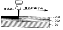
Fig. 2 A is the cutaway view of present embodiment, and by CVD (chemical vapor deposition) method, deposit is the amorphous silicon membrane 203 about the about 50nm~200nm of underlying membrane 202, thickness that is made of silicon oxide film about the about 100nm of thickness for example on insulating properties substrate 201.At this moment, the thickness of the silicon oxide film of amorphous silicon membrane and bottom is not limited to present embodiment.In addition, the structure of underlying membrane 202 can be the stacked film of silicon nitride film or silicon oxide film and silicon nitride film etc.Then, shown in Fig. 2 B and 2C, carry out the crystallization of amorphous silicon film 203, formed single crystalline Si film 204 by laser scanning.Fig. 2 D has represented the section shape in the face vertical with laser scanning of single crystalline Si film 204.At this moment, by laser radiation, amorphous silicon film 203 fusing because condensing of causing of surface tension, has formed a plurality of belt-like single crystal films that the profile construction of each crystalline film is made of an oval-shaped part.In the present embodiment, laser scanning is to use Solid State Laser to scan at certain orientation, but the kind of not special limit laser.In addition, also can for example at first make Si film 203 polycrystallizations, by carrying out scanning, can form monocrystal thin films then based on Solid State Laser by the combination of the different laser of wavelength with excimer laser.
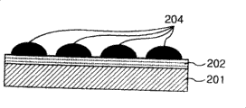
Fig. 3 A, 3B are the characteristic pattern of expression by the single crystalline Si film of this crystallization method formation, and Fig. 3 A has represented the picture of scanning electron microscopy (SEM), and Fig. 3 B has represented the bright-field picture (left side) and the dark field picture (right side) of transmission electron microscope (TEM).As shown in Figure 3A, on the insulating properties substrate, formed the single crystalline Si film 204 of the band shape of extending as can be known in the direction identical with laser scanning direction.Shown in the little figure of Fig. 3 A, these belt-like single crystals Si film is characterised in that: the cross-sectional configuration in the face vertical with length direction is oval.This be because the Si that melts by laser scanning since surface tension condense because the scanning by laser again, in lateral growth crystallization, the belt-like single crystal Si film of just having grown and having had round cross sectional shape.In addition, according to the bright-field picture (left side) of the TEM shown in Fig. 3 B,, do not find observed grain circle in the polycrystalline Si film in the past, and, be the single crystal film that in crystalline film, does not comprise a boundary or defective etc. as can be known according to dark field picture (right side) in the inside of crystalline film.Be that the film that forms in the present embodiment is characterised in that: be formed in the single crystalline Si film of the band shape on the substrate, and the cross-sectional configuration in the face vertical with the length direction of crystalline film has the shape of circular or an oval-shaped part.
(embodiment 2)
In embodiment 2, illustrated in the crystallization step based on laser scanning of explanation in described embodiment 1, specific place on the insulating properties substrate forms the embodiment of single crystalline Si film, promptly for the Position Control of single crystalline Si film at the embodiment that the initial film before the crystallization is carried out composition, with utilization on one side the different underlying membrane of soakage that melts Si is carried out Position Control, Yi Bian form the embodiment of single crystalline Si film.
Fig. 4 A~Fig. 4 G is after explanation forms different shape to amorphous silicon membrane 203, forms the figure of the embodiment of monocrystal thin films by laser radiation.At first, shown in Fig. 4 A, on insulating properties substrate 201, form underlying membrane 202, amorphous silicon film 203, shown in Fig. 4 (B), coating, the exposure of photomask, development, etch process by resist, with the interval of 10 μ m, whole last cycle of described insulating properties substrate formed the belt-like zone of the amorphous silicon film 203 about the about 5 μ m of width after, make this amorphous silicon film 203 crystallizations by laser scanning.If use this method just can form the single crystalline Si film with same widths and length on whole ground of last cycle of substrate.
Additional embodiments as the composition of the amorphous silicon film before the laser scanning 203, shown in Fig. 4 C, both sides in the zone of monocrystallineization, remove part by amorphous silicon film, excavate the hole 205 of rectangle, or shown in Fig. 4 D, make the source of TFT leak between the thickness of Film Thickness Ratio channel region of rectangle amorphous silicon film 206 in zone also thick, excavate the hole of rectangle again in the channel region both sides of this TFT, or shown in Fig. 4 E, have the composition of width regional between the source leakage of TFT than the shape of channel region field width, or as Fig. 4 F, shown in the 4G, after carrying out the composition of shapes such as circle or square,, just can control the position in single crystal film and zone, island by carrying out crystallization.It should be noted that, the width of pattern shown in described 4A~4G, at interval, length etc. can also carry out all changes.In addition, the zone of carrying out composition can be described insulating properties whole area of substrates, perhaps can only carry out composition to the specific place that forms high performance TFT.
Fig. 5 A~5E is explanation by to the underlying membrane utilization of the different film of the soakage of Si of fusing as the Si film, carries out the figure of other embodiment of Position Control in the zone, island of single crystal film.Shown in Fig. 5 A, be configured in the different two kinds of films 207,208 of soakage under the amorphous silicon membrane 203 after, by carrying out laser scanning, shown in Fig. 5 B, the Si of fusing that condensed on the film 207 big to the soakage of Si, the unijunction crystallization just can be controlled the position in the zone, island 204 of single crystalline Si film.In the present embodiment, under amorphous silicon membrane 203, formed the different film of soakage, but as method for distinguishing, also can under amorphous silicon film, form the strong film of soakage 207, the film 208 a little less than the side in the zone, island 203 of the amorphous silicon film that will form pattern forms soakage.In addition, also can on amorphous silicon membrane 203, dispose the different film of soakage.In addition, shown in Fig. 5 C, on whole of substrate, form the strong film 207 of soakage, dispose the island pattern of the weak film 208 of soakage thereon, form amorphous silicon film 203 thereon comprehensively.Then, by carrying out crystallization, shown in Fig. 5 D, between the pattern a little less than the soakage 208, can form zone, single crystal film island 204 based on laser scanning.On the zone, island 204 of this single crystal film, can form thin-film semiconductor device, shown in Fig. 5 E, also can remove film 208 after, form thin-film semiconductor device.
Fig. 6 A~Fig. 6 D is the figure of feature of the cross sectional shape in the zone, single crystalline Si film island that forms on the expression insulating properties substrate.The cross sectional shape in the zone, monocrystal thin films island that forms in the present embodiment as shown in Figure 6A, can by the width (W) in crystallization cross section, thickness (H), radius of curvature (R), with contact angle (θ) definition of substrate.These parameters are by the soakage of thickness, patterning process, Si film and the underlying membrane of the thin film semiconductor on the insulating properties substrate, the surface tension of Si film, the kind and the scan method decision of laser.If represent an example, then use the sample of the thickness of single crystalline Si film as 50nm, undertaken monocrystallineization by laser scanning, obtain about the about 1.0 μ m of W, about the about 100nm of H, about about 30 ° of θ, the belt-like single crystal film about the about 100 μ m of length.It should be noted that present embodiment is not limited to these values,, can obtain the zone, island of more large-area monocrystal thin films by the thickness that changes amorphous silicon, the energy of laser radiation etc.In addition, by on the material of the different film of soakage, the shape of composition etc., working hard, shown in Fig. 6 B~6D, can on the insulating properties substrate, form the zone, island of single crystal film with various cross sectional shapes.
Fig. 7 A, 7B are in the belt-like single crystal Si film that forms in the present embodiment of explanation, based on Fig. 7 A (top) in the result of the analysis of electron ray diffraction approach, the crystal plane orientation that obtains, sum up Fig. 7 B to the crystal orientation of the vertical direction of each crystal plane.When based on the decision in the crystal plane orientation of electron ray diffraction approach, the incident direction of electron beam is for the vertical direction of substrate.In addition,, be necessary to make sample to tilt in ± 5 °, but the inclination in this angle does not exert an influence to the decision in crystal plane orientation for the incident direction of electron beam in order to obtain best crystal orientation.In the analysis result of reality, in the crystal plane orientation of the direction vertical (V-direction) with substrate, all measuring points more than 90% be<110, in addition<100〉and<111 exist at random.Main orientation representation in promptly vertical with the substrate of the monocrystal thin films that forms in the present embodiment direction is<110 〉.In addition, with the result in the face orientation in the cross section of electronics ray diffraction method investigation belt-like single crystal film be laser scanning direction promptly the face orientation of banded length direction (L-direction) be<110 be main directed.In Fig. 7 B, represent the crystal orientation (scan method of L-direction indication laser herein) of L-direction with respect to the crystal orientation of V-direction.For example, if the V-direction be<110, the L-direction vertical with it be<100, or<110 or<111〉direction.
As mentioned above, by use based on laser scanning the initial film before the monocrystallineization is carried out the method for composition, can form the zone, island of single crystalline Si film in specific place, can more improve the surface tension effect, can form high-quality single crystalline Si film.In addition, in the present embodiment, amorphous silicon membrane has been carried out composition, but as other embodiment, also can carry out polycrystallization to amorphous silicon membrane, carry out the composition of polycrystalline Si film then with excimer laser, use solid state laser etc. then, carry out monocrystallineization.In addition,, replace on the insulating properties substrate, forming amorphous silicon membrane as the initial Si film that carries out before the laser scanning, can for example be known as Cat-CVD (catalysis CVD) utilization low temperature CVD method, the substrate of catalyst add the polycrystalline Si film that the hot CVD method forms.After again the polycrystalline Si film that forms with these CVD methods being carried out composition, undertaken monocrystallineization by laser scanning.
(embodiment 3)
Present embodiment illustrates in described embodiment 1 and 2 example that forms thin-film semiconductor device in the single crystal film 204 that the manufacture method of explanation forms, i.e. its component construction and manufacture method with reference to accompanying drawing.
Fig. 8 A is the single crystalline Si film 204 of the band shape that forms on the insulating properties substrate, and having dotted length direction is A, and its vertical direction is B.Fig. 8 B is the figure of the cross-sectional configuration of the MOS type TFT that forms on the belt-like single crystal Si film shown in the key diagram 8A, and direction was consistent with length direction (A direction) between leaked in the source.The figure in left side represents the cross-sectional configuration of A part.On single crystalline Si film 204, form gate insulating film 301, and form single crystalline Si film contact hole 302 and 303, electrode 304 and 305, gate electrode 306, dielectric film 307.In addition, the cross-sectional configuration of the part of the dotted line C that draws to the grid center has been represented on the right side.It is characterized in that: be the channel region that has formed TFT on the oval-shaped single crystalline Si film 204 at cross sectional shape.
Fig. 8 C is the figure of cross-sectional configuration that is illustrated in the TFT of the source that disposed on the direction (B direction) vertical with the length direction of the belt-like single crystal film 204 shown in described Fig. 8 A, drain electrode.In the present embodiment, extend at the length direction (A direction) of belt-like single crystal Si film 204 because be configured to gate electrode 306, thus can make grid width very wide, thus can improve the current driving ability of TFT.
In addition, Fig. 8 D is to use a plurality of described belt-like single crystal Si films 204, constitutes the example of the TFT of raceway groove.In this TFT, can be at the contact hole between leak in formation source on each belt-like single crystal Si film, but as shown in the figure, can be processed into rectangle to the Si film that in the Si film that forms in one side with single crystalline Si film 204 or other layer up and down, forms, in the Si of this rectangle film 320 and 321, contact hole 302 and 303 are set at single crystalline Si film 204.By like this, the damage of the underlying membrane of crossing the single crystalline Si film 204 that etching causes in the time of suppressing the opening of contact hole.In addition, represented the situation of single grid here, but also can adopt TFT structure with a plurality of gate electrodes.In addition, also can use isotropic etching method work sheet epitaxial 204, change circle or plurality of stepped serrations shape, form TFT by before the formation of TFT.
Fig. 8 E is explanation has formed the embodiment of a plurality of TFT310 on described single crystalline Si film 204 figure.In the present embodiment, the area of rectangle single crystalline Si film 204 forms about about 5 μ m * 20 μ m, uses the Micrometer-Nanometer Processing Technology about the about 0.1 μ m of minimum process size, has formed TFT.Can do various changes to the configuration of TFT, the direction of source-drain electrode etc. according to necessity.Like this, the thin-film semiconductor device of a plurality of TFT that formation is made of the single crystalline Si film etc. can be realized integrated circuit.
As other embodiment, forming for example zone, the island monocrystallineization of the amorphous silicon of the shape shown in Fig. 4 D, Fig. 4 E, in the zone, island of this single crystalline Si film, source-drain electrode and grid are set by laser scanning, can form TFT.As mentioned above, the TFT that on the insulating properties substrate, can constitute by the single crystalline Si film with fairly simple method realization.These TFT are high performance, have reliability, and characteristic variations is little, so use these TFT, can be the large scale integrated circuit that forms on the single crystalline Si substrate that is formed on the quartz base plate in the past at complete insulating film substrate.On large tracts of land and cheap glass substrate, can form the image display device of circuit built-in.
It should be noted that present embodiment is the example that forms MOS type TFT, still, because the film of obtaining according to the present invention is the single crystalline Si film, so utilize its speciality, except MOS type TFT, can form for example element of other structures of bipolar transistor etc. certainly.
(embodiment 4)
Below, the thin-film semiconductor device that is made of the single crystalline Si film shown in the described embodiment 1~3, for example embodiment of MOS type TFT have been used in explanation in image display device with reference to Fig. 9 A, 9B.Present embodiment is a system on the panel that has carried systems such as the image display device that is made of liquid crystal and organic EL, the drive circuit that is used to drive it, DAC circuit, power circuit, logical circuit, frame memory on the same substrate.These circuit are to constitute by having implemented TFT of the present invention, form TFT on same glass substrate, so the manufacturing process temperature is for for example below 500 ℃.
If it is the manufacturing process of TFT is described, then as described below.At first, shown in Fig. 9 A, deposited amorphous silicon thin film 203 on cheap large-scale insulating properties substrate 201 such as for example glass or plastics etc. is whole of excimer laser scanning substrate by first laser step for example, has formed the polycrystalline Si film.Then, carry out the composition of polycrystalline Si film according to necessity to forming the zone 401 of the circuit of the display element array part periphery of drive circuit, D/A conversion circuit, power circuit, logical circuit, frame memory etc. for example, by the i.e. Solid State Laser for example of second laser step, carry out laser scanning once again, in zone 401, form the TFT that constitutes by the single crystalline Si film with method of the present invention, constituted necessary circuit.
Described crystallization step is to make whole crystallization of substrate by excimer laser, only makes peripheral circuit area 401 once again by the laser scanning monocrystallineization, but also can be method for distinguishing.For example, behind the deposited amorphous silicon thin film, undertaken monocrystallineization, be not only peripheral circuit area, also form the TFT that constitutes by peripheral circuit area, form the pixel built-in circuit of pixel TFT and pixel store etc. in the display element array part by comprehensive laser scanning.In addition,, passing through for example comprehensive deposit of CVD method behind the polycrystalline Si film,, forming the TFT that constitutes by the single crystalline Si film by laser scanning selectively only in the place that forms peripheral circuit area in order to omit the laser scanning step as possible.
Fig. 9 B is the plane model figure that the apparatus structure of system on the panel of the TFT that is formed by described manufacturing process has been used in expression.The high performance TFT that constitutes by the single crystalline Si film in the periphery setting of image displaying part 410, the peripheral circuit of configuration frame memory, picture signal driving system circuit 411, vertical scan system circuit 412, logical circuit 413, interface circuit 414, power circuit 415, DAC circuit 416 etc., by 417 these peripheral circuits of connection and the pixel circuits that connect up, constituted system on the panel.According to enforcement of the present invention, can obtain the system on the panel of high image quality, low power consumption, highly reliable, slim, light weight.
(embodiment 5)
Present embodiment is an electronic instrument of having used system on the panel shown in the described embodiment 4, and Figure 10 has represented its form.For example can be applied to display, mobile phone, portable data assistance various electronic instruments such as (PDA) that slim large-screen TV, PC use, and by utilizing TFT of the present invention, the peripheral circuit that in the past is made of the installation of LSI is built on the same substrate, the speciality of high image quality, low power consumption, highly reliable, slim, light weight can be merged, cost degradation can be realized.
According to the present invention, can be at low temperatures, the thin-film semiconductor device of the TFT that formation is made of the single crystalline Si film on the insulating properties substrate etc. can be realized the image display device (system on the panel) of the system of having carried and the integrated circuit on the complete insulating properties substrate.
Claims (5)
1. thin-film semiconductor device has: insulating properties substrate and be arranged on isolated zone, monocrystal thin films island on this insulating properties substrate,
Wherein, zone, described monocrystal thin films island is the belt-like single crystal film, the cross section vertical with substrate in zone, described monocrystal thin films island has subcircular, near oval or by the cross sectional shape that their part constitutes, and is formed with the active region of thin-film transistor in this zone, monocrystal thin films island.
2. thin-film semiconductor device according to claim 1, wherein: the source of described thin-film transistor, leakage direction are configured near parallel or near vertical with the length direction of described belt-like single crystal film.
3. thin-film semiconductor device according to claim 1, wherein: in the active region of described thin-film transistor, comprise more than one described belt-like single crystal film at least.
4. thin-film semiconductor device according to claim 1, wherein: the active region that in described belt-like single crystal film, is formed with the above thin-film transistor at least.
5. thin-film semiconductor device according to claim 1, wherein: this thin-film semiconductor device is made of insulating properties substrate and the zone, monocrystal thin films island that is arranged on the described insulating properties substrate, this zone, monocrystal thin films island, with the primary crystallization orientation of the perpendicular direction of this substrate be<110, and with respect to this substrate be the crystal orientation of the length direction in horizontal direction and this zone, monocrystal thin films island be<100.
Applications Claiming Priority (2)
| Application Number | Priority Date | Filing Date | Title |
|---|---|---|---|
| JP2002192852A JP4329312B2 (en) | 2002-07-02 | 2002-07-02 | Thin film semiconductor device, manufacturing method thereof, and image display device |
| JP192852/2002 | 2002-07-02 |
Publications (2)
| Publication Number | Publication Date |
|---|---|
| CN1467859A CN1467859A (en) | 2004-01-14 |
| CN100456497C true CN100456497C (en) | 2009-01-28 |
Family
ID=29996983
Family Applications (1)
| Application Number | Title | Priority Date | Filing Date |
|---|---|---|---|
| CNB031199097A Expired - Fee Related CN100456497C (en) | 2002-07-02 | 2003-02-28 | Thin-film semiconductor device, manufacturing method of the same and image display apparatus |
Country Status (5)
| Country | Link |
|---|---|
| US (2) | US6847069B2 (en) |
| JP (1) | JP4329312B2 (en) |
| KR (1) | KR100998148B1 (en) |
| CN (1) | CN100456497C (en) |
| TW (1) | TWI266371B (en) |
Families Citing this family (14)
| Publication number | Priority date | Publication date | Assignee | Title |
|---|---|---|---|---|
| US7732334B2 (en) * | 2004-08-23 | 2010-06-08 | Semiconductor Energy Laboratory Co., Ltd. | Method for manufacturing semiconductor device |
| CN100592520C (en) * | 2004-10-22 | 2010-02-24 | 株式会社半导体能源研究所 | Semiconductor device and display device comprising same |
| JP2006128233A (en) | 2004-10-27 | 2006-05-18 | Hitachi Ltd | Semiconductor material, field effect transistor, and manufacturing method thereof |
| KR100570219B1 (en) * | 2004-12-23 | 2006-04-12 | 주식회사 하이닉스반도체 | Double gate line of the semiconductor and method for manufacturing thereof |
| JP2006261188A (en) * | 2005-03-15 | 2006-09-28 | Seiko Epson Corp | Semiconductor device and its manufacturing method |
| US8022408B2 (en) | 2005-05-13 | 2011-09-20 | Samsung Electronics Co., Ltd. | Crystalline nanowire substrate, method of manufacturing the same, and method of manufacturing thin film transistor using the same |
| KR101127132B1 (en) * | 2005-05-13 | 2012-03-21 | 삼성전자주식회사 | Si nanowire substrate and fabrication method of the same, and fabrication method of thin film transistor using the same |
| JP4850452B2 (en) * | 2005-08-08 | 2012-01-11 | 株式会社 日立ディスプレイズ | Image display device |
| US20090250700A1 (en) * | 2008-04-08 | 2009-10-08 | Themistokles Afentakis | Crystalline Semiconductor Stripe Transistor |
| US20090250791A1 (en) * | 2008-04-08 | 2009-10-08 | Themistokles Afentakis | Crystalline Semiconductor Stripes |
| JP5669439B2 (en) * | 2010-05-21 | 2015-02-12 | 株式会社半導体エネルギー研究所 | Method for manufacturing semiconductor substrate |
| CN102280474B (en) * | 2010-06-09 | 2014-02-19 | 尹海洲 | IGBT (insulated-gate bipolar transistor) device and manufacturing method thereof |
| GB201310854D0 (en) | 2013-06-18 | 2013-07-31 | Isis Innovation | Photoactive layer production process |
| JP6857517B2 (en) * | 2016-06-16 | 2021-04-14 | ディフテック レーザーズ インコーポレイテッド | How to make crystalline islands on a substrate |
Citations (5)
| Publication number | Priority date | Publication date | Assignee | Title |
|---|---|---|---|---|
| JPH08316485A (en) * | 1995-05-12 | 1996-11-29 | Fuji Xerox Co Ltd | Formation of semiconductor crystal and manufacture of semiconductor device using this |
| JPH08340118A (en) * | 1995-06-09 | 1996-12-24 | Sony Corp | Manufacture of thin film semiconductor device |
| CN1152792A (en) * | 1992-12-04 | 1997-06-25 | 株式会社半导体能源研究所 | Semiconductor device and making process |
| US5808321A (en) * | 1993-06-12 | 1998-09-15 | Semiconductor Energy Laboratory Co., Ltd. | Semiconductor device with recrystallized active area |
| EP1054452A2 (en) * | 1999-05-15 | 2000-11-22 | Semiconductor Energy Laboratory Co., Ltd. | TFT and method for its fabrication |
Family Cites Families (8)
| Publication number | Priority date | Publication date | Assignee | Title |
|---|---|---|---|---|
| JP3213338B2 (en) * | 1991-05-15 | 2001-10-02 | 株式会社リコー | Manufacturing method of thin film semiconductor device |
| JPH10289876A (en) * | 1997-04-16 | 1998-10-27 | Hitachi Ltd | Laser crystallizing method, semiconductor device formed thereby, and applied equipment |
| JPH11121753A (en) | 1997-10-14 | 1999-04-30 | Hitachi Ltd | Semiconductor device and manufacture thereof |
| JP2000243970A (en) | 1999-02-24 | 2000-09-08 | Matsushita Electric Ind Co Ltd | Thin film transistor, manufacture thereof, liquid crystal display device using the same and manufacture thereof |
| US6271101B1 (en) * | 1998-07-29 | 2001-08-07 | Semiconductor Energy Laboratory Co., Ltd. | Process for production of SOI substrate and process for production of semiconductor device |
| JP2001345451A (en) * | 2000-05-30 | 2001-12-14 | Hitachi Ltd | Thin-film semiconductor integrated-circuit device, and picture display using the same, and their manufacturing methods |
| US6580122B1 (en) * | 2001-03-20 | 2003-06-17 | Advanced Micro Devices, Inc. | Transistor device having an enhanced width dimension and a method of making same |
| US6692999B2 (en) * | 2001-06-26 | 2004-02-17 | Fujitsu Limited | Polysilicon film forming method |
-
2002
- 2002-07-02 JP JP2002192852A patent/JP4329312B2/en not_active Expired - Fee Related
-
2003
- 2003-02-25 TW TW092103932A patent/TWI266371B/en not_active IP Right Cessation
- 2003-02-26 US US10/372,809 patent/US6847069B2/en not_active Expired - Fee Related
- 2003-02-27 KR KR1020030012276A patent/KR100998148B1/en not_active IP Right Cessation
- 2003-02-28 CN CNB031199097A patent/CN100456497C/en not_active Expired - Fee Related
-
2004
- 2004-12-07 US US11/004,858 patent/US7084020B2/en not_active Expired - Fee Related
Patent Citations (5)
| Publication number | Priority date | Publication date | Assignee | Title |
|---|---|---|---|---|
| CN1152792A (en) * | 1992-12-04 | 1997-06-25 | 株式会社半导体能源研究所 | Semiconductor device and making process |
| US5808321A (en) * | 1993-06-12 | 1998-09-15 | Semiconductor Energy Laboratory Co., Ltd. | Semiconductor device with recrystallized active area |
| JPH08316485A (en) * | 1995-05-12 | 1996-11-29 | Fuji Xerox Co Ltd | Formation of semiconductor crystal and manufacture of semiconductor device using this |
| JPH08340118A (en) * | 1995-06-09 | 1996-12-24 | Sony Corp | Manufacture of thin film semiconductor device |
| EP1054452A2 (en) * | 1999-05-15 | 2000-11-22 | Semiconductor Energy Laboratory Co., Ltd. | TFT and method for its fabrication |
Also Published As
| Publication number | Publication date |
|---|---|
| US7084020B2 (en) | 2006-08-01 |
| CN1467859A (en) | 2004-01-14 |
| US20050095822A1 (en) | 2005-05-05 |
| JP2004039765A (en) | 2004-02-05 |
| KR20040004039A (en) | 2004-01-13 |
| KR100998148B1 (en) | 2010-12-02 |
| JP4329312B2 (en) | 2009-09-09 |
| TWI266371B (en) | 2006-11-11 |
| TW200401366A (en) | 2004-01-16 |
| US20040005747A1 (en) | 2004-01-08 |
| US6847069B2 (en) | 2005-01-25 |
Similar Documents
| Publication | Publication Date | Title |
|---|---|---|
| CN100456497C (en) | Thin-film semiconductor device, manufacturing method of the same and image display apparatus | |
| CN100356506C (en) | Crystal mask, amorphous silicon crystallization method and method of manufacturing array base plate using same | |
| JP4358998B2 (en) | Thin film transistor device and manufacturing method thereof | |
| JP2001023899A (en) | Semiconductor thin film, liquid crystal display device provided with the same, and manufacture of the film | |
| TW535295B (en) | Method for crystallizing a silicon layer and fabricating a TFT using the same | |
| KR101243667B1 (en) | Polysilicon liquid crystal display device and method for fabricating thereof | |
| CN1577772A (en) | Method of fabricating bottom-gated polycrystalline silicon thin film transistor | |
| US20060113596A1 (en) | Single crystal substrate and method of fabricating the same | |
| CN1312523C (en) | Liquid crystal display device and method of fabricating the same | |
| US4868140A (en) | Semiconductor device and method of manufacturing the same | |
| KR100783224B1 (en) | Thin-film semiconductor integrated circuit device and picture display device with using thereof and manufacturing method thereof | |
| TWI527087B (en) | Polysilicon layer, method of preparing the polysilicon layer, thin film transistor using the polysilicon layer, and organic light emitting display device including the thin film transistor | |
| KR100628989B1 (en) | Crystallization method of amorphous silicon thin film | |
| CN203367290U (en) | Thin film transistor array substrate and liquid crystal display | |
| KR100366959B1 (en) | crystallization method | |
| CN100372119C (en) | Semiconductor structure with composite polysilicon layer and displaying panel therefor | |
| KR20020032196A (en) | Polysilicon-thin film transistor device and method of fabricating the same | |
| JP2000183357A (en) | Thin film transistor and manufacture thereof | |
| KR100275206B1 (en) | Method for manufacturing poly-silicon single electron device via excimer-laser irradiation | |
| CN100573284C (en) | Liquid crystal disply device and its preparation method | |
| KR100709282B1 (en) | The manafacturing method of the silicon thin film transistor | |
| Lee et al. | Influences of directional crystallization using field aided lateral crystallization on the electrical characteristics of poly-Si thin film transistors | |
| JPH11284191A (en) | Vertical type thin-film transistor and its manufacture | |
| KR20080098978A (en) | A formation method of doped polysilicon thin films through a energy transport layer | |
| JPS59150478A (en) | Thin film circuit device |
Legal Events
| Date | Code | Title | Description |
|---|---|---|---|
| C06 | Publication | ||
| PB01 | Publication | ||
| C10 | Entry into substantive examination | ||
| SE01 | Entry into force of request for substantive examination | ||
| C14 | Grant of patent or utility model | ||
| GR01 | Patent grant | ||
| C17 | Cessation of patent right | ||
| CF01 | Termination of patent right due to non-payment of annual fee |
Granted publication date: 20090128 Termination date: 20130228 |