CN100451914C - Phase locked loop fast power up methods and apparatus - Google Patents
Phase locked loop fast power up methods and apparatus Download PDFInfo
- Publication number
- CN100451914C CN100451914C CNB028169697A CN02816969A CN100451914C CN 100451914 C CN100451914 C CN 100451914C CN B028169697 A CNB028169697 A CN B028169697A CN 02816969 A CN02816969 A CN 02816969A CN 100451914 C CN100451914 C CN 100451914C
- Authority
- CN
- China
- Prior art keywords
- frequency
- clock signal
- signal
- multiplier
- processor
- Prior art date
- Legal status (The legal status is an assumption and is not a legal conclusion. Google has not performed a legal analysis and makes no representation as to the accuracy of the status listed.)
- Expired - Lifetime
Links
- 238000000034 method Methods 0.000 title claims description 28
- 230000001360 synchronised effect Effects 0.000 claims description 15
- 230000033228 biological regulation Effects 0.000 claims description 5
- 238000012544 monitoring process Methods 0.000 claims description 3
- 230000000630 rising effect Effects 0.000 claims description 2
- 238000012545 processing Methods 0.000 description 9
- 238000010586 diagram Methods 0.000 description 7
- 230000006870 function Effects 0.000 description 7
- 230000008859 change Effects 0.000 description 4
- 238000012937 correction Methods 0.000 description 4
- 238000013016 damping Methods 0.000 description 4
- 230000003213 activating effect Effects 0.000 description 3
- 230000001934 delay Effects 0.000 description 3
- 230000009471 action Effects 0.000 description 2
- 230000004913 activation Effects 0.000 description 2
- 238000013461 design Methods 0.000 description 2
- 230000005059 dormancy Effects 0.000 description 2
- 230000006872 improvement Effects 0.000 description 2
- GOLXNESZZPUPJE-UHFFFAOYSA-N spiromesifen Chemical compound CC1=CC(C)=CC(C)=C1C(C(O1)=O)=C(OC(=O)CC(C)(C)C)C11CCCC1 GOLXNESZZPUPJE-UHFFFAOYSA-N 0.000 description 2
- 239000013078 crystal Substances 0.000 description 1
- 230000003111 delayed effect Effects 0.000 description 1
- 238000001514 detection method Methods 0.000 description 1
- 238000005516 engineering process Methods 0.000 description 1
- 238000001914 filtration Methods 0.000 description 1
- 230000005764 inhibitory process Effects 0.000 description 1
- 230000000266 injurious effect Effects 0.000 description 1
- 238000012423 maintenance Methods 0.000 description 1
- 230000007246 mechanism Effects 0.000 description 1
- 230000002093 peripheral effect Effects 0.000 description 1
- 230000001915 proofreading effect Effects 0.000 description 1
- 230000001105 regulatory effect Effects 0.000 description 1
Images


Classifications
-
- G—PHYSICS
- G06—COMPUTING; CALCULATING OR COUNTING
- G06F—ELECTRIC DIGITAL DATA PROCESSING
- G06F11/00—Error detection; Error correction; Monitoring
- G06F11/36—Preventing errors by testing or debugging software
- G06F11/362—Software debugging
- G06F11/3636—Software debugging by tracing the execution of the program
-
- G—PHYSICS
- G06—COMPUTING; CALCULATING OR COUNTING
- G06F—ELECTRIC DIGITAL DATA PROCESSING
- G06F1/00—Details not covered by groups G06F3/00 - G06F13/00 and G06F21/00
- G06F1/04—Generating or distributing clock signals or signals derived directly therefrom
-
- G—PHYSICS
- G06—COMPUTING; CALCULATING OR COUNTING
- G06F—ELECTRIC DIGITAL DATA PROCESSING
- G06F1/00—Details not covered by groups G06F3/00 - G06F13/00 and G06F21/00
- G06F1/04—Generating or distributing clock signals or signals derived directly therefrom
- G06F1/08—Clock generators with changeable or programmable clock frequency
-
- G—PHYSICS
- G06—COMPUTING; CALCULATING OR COUNTING
- G06F—ELECTRIC DIGITAL DATA PROCESSING
- G06F1/00—Details not covered by groups G06F3/00 - G06F13/00 and G06F21/00
- G06F1/26—Power supply means, e.g. regulation thereof
- G06F1/32—Means for saving power
- G06F1/3203—Power management, i.e. event-based initiation of a power-saving mode
- G06F1/3234—Power saving characterised by the action undertaken
- G06F1/3237—Power saving characterised by the action undertaken by disabling clock generation or distribution
-
- G—PHYSICS
- G06—COMPUTING; CALCULATING OR COUNTING
- G06F—ELECTRIC DIGITAL DATA PROCESSING
- G06F1/00—Details not covered by groups G06F3/00 - G06F13/00 and G06F21/00
- G06F1/26—Power supply means, e.g. regulation thereof
- G06F1/32—Means for saving power
- G06F1/3203—Power management, i.e. event-based initiation of a power-saving mode
- G06F1/3234—Power saving characterised by the action undertaken
- G06F1/324—Power saving characterised by the action undertaken by lowering clock frequency
-
- G—PHYSICS
- G06—COMPUTING; CALCULATING OR COUNTING
- G06F—ELECTRIC DIGITAL DATA PROCESSING
- G06F1/00—Details not covered by groups G06F3/00 - G06F13/00 and G06F21/00
- G06F1/26—Power supply means, e.g. regulation thereof
- G06F1/32—Means for saving power
- G06F1/3203—Power management, i.e. event-based initiation of a power-saving mode
- G06F1/3234—Power saving characterised by the action undertaken
- G06F1/3287—Power saving characterised by the action undertaken by switching off individual functional units in the computer system
-
- G—PHYSICS
- G06—COMPUTING; CALCULATING OR COUNTING
- G06F—ELECTRIC DIGITAL DATA PROCESSING
- G06F1/00—Details not covered by groups G06F3/00 - G06F13/00 and G06F21/00
- G06F1/26—Power supply means, e.g. regulation thereof
- G06F1/32—Means for saving power
- G06F1/3203—Power management, i.e. event-based initiation of a power-saving mode
- G06F1/3234—Power saving characterised by the action undertaken
- G06F1/3296—Power saving characterised by the action undertaken by lowering the supply or operating voltage
-
- G—PHYSICS
- G06—COMPUTING; CALCULATING OR COUNTING
- G06F—ELECTRIC DIGITAL DATA PROCESSING
- G06F12/00—Accessing, addressing or allocating within memory systems or architectures
- G06F12/02—Addressing or allocation; Relocation
- G06F12/08—Addressing or allocation; Relocation in hierarchically structured memory systems, e.g. virtual memory systems
- G06F12/0802—Addressing of a memory level in which the access to the desired data or data block requires associative addressing means, e.g. caches
- G06F12/0806—Multiuser, multiprocessor or multiprocessing cache systems
- G06F12/0842—Multiuser, multiprocessor or multiprocessing cache systems for multiprocessing or multitasking
-
- G—PHYSICS
- G06—COMPUTING; CALCULATING OR COUNTING
- G06F—ELECTRIC DIGITAL DATA PROCESSING
- G06F13/00—Interconnection of, or transfer of information or other signals between, memories, input/output devices or central processing units
- G06F13/14—Handling requests for interconnection or transfer
- G06F13/20—Handling requests for interconnection or transfer for access to input/output bus
- G06F13/28—Handling requests for interconnection or transfer for access to input/output bus using burst mode transfer, e.g. direct memory access DMA, cycle steal
-
- G—PHYSICS
- G06—COMPUTING; CALCULATING OR COUNTING
- G06F—ELECTRIC DIGITAL DATA PROCESSING
- G06F13/00—Interconnection of, or transfer of information or other signals between, memories, input/output devices or central processing units
- G06F13/38—Information transfer, e.g. on bus
- G06F13/382—Information transfer, e.g. on bus using universal interface adapter
- G06F13/385—Information transfer, e.g. on bus using universal interface adapter for adaptation of a particular data processing system to different peripheral devices
-
- G—PHYSICS
- G06—COMPUTING; CALCULATING OR COUNTING
- G06F—ELECTRIC DIGITAL DATA PROCESSING
- G06F9/00—Arrangements for program control, e.g. control units
- G06F9/06—Arrangements for program control, e.g. control units using stored programs, i.e. using an internal store of processing equipment to receive or retain programs
- G06F9/30—Arrangements for executing machine instructions, e.g. instruction decode
- G06F9/38—Concurrent instruction execution, e.g. pipeline, look ahead
- G06F9/3836—Instruction issuing, e.g. dynamic instruction scheduling or out of order instruction execution
- G06F9/3851—Instruction issuing, e.g. dynamic instruction scheduling or out of order instruction execution from multiple instruction streams, e.g. multistreaming
-
- G—PHYSICS
- G06—COMPUTING; CALCULATING OR COUNTING
- G06F—ELECTRIC DIGITAL DATA PROCESSING
- G06F9/00—Arrangements for program control, e.g. control units
- G06F9/06—Arrangements for program control, e.g. control units using stored programs, i.e. using an internal store of processing equipment to receive or retain programs
- G06F9/30—Arrangements for executing machine instructions, e.g. instruction decode
- G06F9/38—Concurrent instruction execution, e.g. pipeline, look ahead
- G06F9/3867—Concurrent instruction execution, e.g. pipeline, look ahead using instruction pipelines
- G06F9/3869—Implementation aspects, e.g. pipeline latches; pipeline synchronisation and clocking
-
- G—PHYSICS
- G06—COMPUTING; CALCULATING OR COUNTING
- G06F—ELECTRIC DIGITAL DATA PROCESSING
- G06F9/00—Arrangements for program control, e.g. control units
- G06F9/06—Arrangements for program control, e.g. control units using stored programs, i.e. using an internal store of processing equipment to receive or retain programs
- G06F9/46—Multiprogramming arrangements
- G06F9/48—Program initiating; Program switching, e.g. by interrupt
- G06F9/4806—Task transfer initiation or dispatching
- G06F9/4843—Task transfer initiation or dispatching by program, e.g. task dispatcher, supervisor, operating system
-
- H—ELECTRICITY
- H03—ELECTRONIC CIRCUITRY
- H03L—AUTOMATIC CONTROL, STARTING, SYNCHRONISATION, OR STABILISATION OF GENERATORS OF ELECTRONIC OSCILLATIONS OR PULSES
- H03L7/00—Automatic control of frequency or phase; Synchronisation
- H03L7/06—Automatic control of frequency or phase; Synchronisation using a reference signal applied to a frequency- or phase-locked loop
- H03L7/08—Details of the phase-locked loop
- H03L7/0802—Details of the phase-locked loop the loop being adapted for reducing power consumption
-
- H—ELECTRICITY
- H03—ELECTRONIC CIRCUITRY
- H03L—AUTOMATIC CONTROL, STARTING, SYNCHRONISATION, OR STABILISATION OF GENERATORS OF ELECTRONIC OSCILLATIONS OR PULSES
- H03L7/00—Automatic control of frequency or phase; Synchronisation
- H03L7/06—Automatic control of frequency or phase; Synchronisation using a reference signal applied to a frequency- or phase-locked loop
- H03L7/16—Indirect frequency synthesis, i.e. generating a desired one of a number of predetermined frequencies using a frequency- or phase-locked loop
- H03L7/18—Indirect frequency synthesis, i.e. generating a desired one of a number of predetermined frequencies using a frequency- or phase-locked loop using a frequency divider or counter in the loop
- H03L7/183—Indirect frequency synthesis, i.e. generating a desired one of a number of predetermined frequencies using a frequency- or phase-locked loop using a frequency divider or counter in the loop a time difference being used for locking the loop, the counter counting between fixed numbers or the frequency divider dividing by a fixed number
-
- G—PHYSICS
- G06—COMPUTING; CALCULATING OR COUNTING
- G06F—ELECTRIC DIGITAL DATA PROCESSING
- G06F12/00—Accessing, addressing or allocating within memory systems or architectures
- G06F12/02—Addressing or allocation; Relocation
- G06F12/08—Addressing or allocation; Relocation in hierarchically structured memory systems, e.g. virtual memory systems
- G06F12/0802—Addressing of a memory level in which the access to the desired data or data block requires associative addressing means, e.g. caches
- G06F12/0844—Multiple simultaneous or quasi-simultaneous cache accessing
- G06F12/0855—Overlapped cache accessing, e.g. pipeline
- G06F12/0859—Overlapped cache accessing, e.g. pipeline with reload from main memory
-
- G—PHYSICS
- G06—COMPUTING; CALCULATING OR COUNTING
- G06F—ELECTRIC DIGITAL DATA PROCESSING
- G06F2213/00—Indexing scheme relating to interconnection of, or transfer of information or other signals between, memories, input/output devices or central processing units
- G06F2213/38—Universal adapter
- G06F2213/3814—Wireless link with a computer system port
-
- H—ELECTRICITY
- H03—ELECTRONIC CIRCUITRY
- H03L—AUTOMATIC CONTROL, STARTING, SYNCHRONISATION, OR STABILISATION OF GENERATORS OF ELECTRONIC OSCILLATIONS OR PULSES
- H03L7/00—Automatic control of frequency or phase; Synchronisation
- H03L7/06—Automatic control of frequency or phase; Synchronisation using a reference signal applied to a frequency- or phase-locked loop
- H03L7/08—Details of the phase-locked loop
- H03L7/085—Details of the phase-locked loop concerning mainly the frequency- or phase-detection arrangement including the filtering or amplification of its output signal
- H03L7/095—Details of the phase-locked loop concerning mainly the frequency- or phase-detection arrangement including the filtering or amplification of its output signal using a lock detector
-
- H—ELECTRICITY
- H04—ELECTRIC COMMUNICATION TECHNIQUE
- H04W—WIRELESS COMMUNICATION NETWORKS
- H04W88/00—Devices specially adapted for wireless communication networks, e.g. terminals, base stations or access point devices
- H04W88/02—Terminal devices
- H04W88/06—Terminal devices adapted for operation in multiple networks or having at least two operational modes, e.g. multi-mode terminals
-
- Y—GENERAL TAGGING OF NEW TECHNOLOGICAL DEVELOPMENTS; GENERAL TAGGING OF CROSS-SECTIONAL TECHNOLOGIES SPANNING OVER SEVERAL SECTIONS OF THE IPC; TECHNICAL SUBJECTS COVERED BY FORMER USPC CROSS-REFERENCE ART COLLECTIONS [XRACs] AND DIGESTS
- Y02—TECHNOLOGIES OR APPLICATIONS FOR MITIGATION OR ADAPTATION AGAINST CLIMATE CHANGE
- Y02D—CLIMATE CHANGE MITIGATION TECHNOLOGIES IN INFORMATION AND COMMUNICATION TECHNOLOGIES [ICT], I.E. INFORMATION AND COMMUNICATION TECHNOLOGIES AIMING AT THE REDUCTION OF THEIR OWN ENERGY USE
- Y02D10/00—Energy efficient computing, e.g. low power processors, power management or thermal management
-
- Y—GENERAL TAGGING OF NEW TECHNOLOGICAL DEVELOPMENTS; GENERAL TAGGING OF CROSS-SECTIONAL TECHNOLOGIES SPANNING OVER SEVERAL SECTIONS OF THE IPC; TECHNICAL SUBJECTS COVERED BY FORMER USPC CROSS-REFERENCE ART COLLECTIONS [XRACs] AND DIGESTS
- Y02—TECHNOLOGIES OR APPLICATIONS FOR MITIGATION OR ADAPTATION AGAINST CLIMATE CHANGE
- Y02D—CLIMATE CHANGE MITIGATION TECHNOLOGIES IN INFORMATION AND COMMUNICATION TECHNOLOGIES [ICT], I.E. INFORMATION AND COMMUNICATION TECHNOLOGIES AIMING AT THE REDUCTION OF THEIR OWN ENERGY USE
- Y02D30/00—Reducing energy consumption in communication networks
- Y02D30/50—Reducing energy consumption in communication networks in wire-line communication networks, e.g. low power modes or reduced link rate
-
- Y—GENERAL TAGGING OF NEW TECHNOLOGICAL DEVELOPMENTS; GENERAL TAGGING OF CROSS-SECTIONAL TECHNOLOGIES SPANNING OVER SEVERAL SECTIONS OF THE IPC; TECHNICAL SUBJECTS COVERED BY FORMER USPC CROSS-REFERENCE ART COLLECTIONS [XRACs] AND DIGESTS
- Y02—TECHNOLOGIES OR APPLICATIONS FOR MITIGATION OR ADAPTATION AGAINST CLIMATE CHANGE
- Y02D—CLIMATE CHANGE MITIGATION TECHNOLOGIES IN INFORMATION AND COMMUNICATION TECHNOLOGIES [ICT], I.E. INFORMATION AND COMMUNICATION TECHNOLOGIES AIMING AT THE REDUCTION OF THEIR OWN ENERGY USE
- Y02D30/00—Reducing energy consumption in communication networks
- Y02D30/70—Reducing energy consumption in communication networks in wireless communication networks
-
- Y—GENERAL TAGGING OF NEW TECHNOLOGICAL DEVELOPMENTS; GENERAL TAGGING OF CROSS-SECTIONAL TECHNOLOGIES SPANNING OVER SEVERAL SECTIONS OF THE IPC; TECHNICAL SUBJECTS COVERED BY FORMER USPC CROSS-REFERENCE ART COLLECTIONS [XRACs] AND DIGESTS
- Y10—TECHNICAL SUBJECTS COVERED BY FORMER USPC
- Y10S—TECHNICAL SUBJECTS COVERED BY FORMER USPC CROSS-REFERENCE ART COLLECTIONS [XRACs] AND DIGESTS
- Y10S331/00—Oscillators
- Y10S331/02—Phase locked loop having lock indicating or detecting means
Abstract
A PLL frequency multiplier is provided having a latency substantially equal to the wake-up time of the PLL. An operative clock signal is provided to a processor while the PLL is acquiring phase lock by insuring that the clock signal does not contain frequencies above a target frequency of a PLL and below a predetermined threshold frequency. In particular, a frquency divider and a frequency detector are provided to prevent the frequency of the clock signall from operating outside the range defined by the threshold and target frequencies.
Description
Related application
It is 60/315,655 by the application number of submissions such as Allen on 35U.S.C. § 119 (e) basis that the application requires August 29 calendar year 2001, and title is the rights and interests of the provisional application of " DIGITAL BASEBANDPROCESSOR ".Whole merging of above provisional application are in this application with for referencial use.
Technical field
The present invention relates to phaselocked loop (PLL) frequency multiplier, especially for provide operation clock signal to reduce the method and apparatus of the consumption relevant by interim locking time with activating PLL at PLL.
Background technology
Among many computing systems, digital device etc., often the various clock signals that processor is needed are synchronized to single reference clock signal, are assigned to the suitable logical circuit of processor, subsystem and element then.Term " processor " is often referred to the equipment of any actuating logic computing, calculation task and/or control function.Processor can comprise one or more subsystems, element and/or other processors.Processor generally comprises various logic and/or digital element, and they utilize clock signal to operate, be used for latch data, advance and/or the logic state that sorts, calculating synchronously and logical operation and/or other timing functions are provided.
For example, portable phone comprises the processor with a plurality of subsystems or element, and such as digital signal processor (DSP), it moves with high clock frequency, is used for carrying out in real time, computation-intensive and often be the task of time strictness; Microcontroller (MCU) with low clock frequency action, is for example carried out various control function, coordination incident, executive system software or the like.In addition, DSP and MCU can operate or have the supporting element with a plurality of clock frequency actions separately.The computation requirement that depends on processor in the demand of any fixed time clock frequency.
The frequency multiplier of being realized by analog or digital phaselocked loop (PLL) or delay lock loop (DLL) is through being commonly used to generate high frequency clock signal, and be locked into the reference clock homophase.Then this high frequency clock signal can provide be used for drive logic or element, offer the clock distribution tree of digital device and/or distribute to the timing demand that processor satisfies system in addition.Like this, the clock frequency demand of the various elements of processor can and be synchronized to single reference signal by single reference signal support.
Provide term in the clock signal " to provide " to describe signal do not have disabled, by bypass, be under an embargo (gated off) or be prevented from being applied to logic gate, digital element and/or the circuit etc. of indication, or by its reception and be used for operation.Usually, term clock element will be with describing any above-mentioned element here.For example, clock signal can offer bypass and select, forbids logic, clock distribution tree or the like, but finally offers one or more such as the low level element of needs such as logic gate, trigger as logic level, timing signal, latch etc.The set of these low level elements or this low level element is commonly called the clock element.
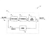
Fig. 1 is the block diagram that generates the existing frequency multiplier 10 of clock signal from input clock signal.Frequency multiplier 10 comprises PLL 12, and this PLL 12 generates high frequency clock signal 32 and locks this signal and input clock signal 30 homophases.
Term clock signal or simple clock typically refer to any analog or digital cyclical signal, especially are used for generating into logic element, digital circuit or other (that is clock element) cyclical signal of at least one timing signal or logic level.Clock signal can be any in the various waveforms, and these waveforms are including but not limited to sine wave, square wave, train of impulses etc.For example, clock signal can be the signal of final state as the processor that advances, locking data, actuating logic operation etc.Also may be thought of as clock signal such as the sinusoidal wave signal of swing (swing) with from the signal of the crystal oscillator that for example therefrom forms and/or derive one or more clock signals.
Voltage controlled oscillator (VCO) is generally oscillator provides voltage, and the signal that has with the proportional frequency of voltage that provides is provided this oscillator.Like this, the voltage correction signal 42 that VCO 26 receives from loop filter 24, and correspondingly adjust the voltage that offers oscillator.Thereby adjust the frequency of clock signal 32, to proofread and correct by phase comparator 22 detected phase errors (being that clock signal 32 is improved to and input clock signal 30 homophases).
The clock signal of generally following generation to be phase-locked to input clock signal has various delays.Particularly the phaselocked loop convergence needs certain hour (that is, locking clock signal and input clock signal homophase) at interval.The delay that takes place when obtaining phase locking often is called locking time.
When Fig. 2 is phase-locked to the clock signal of input clock signal for diagram utilization frequency multiplier as shown in Figure 1 produces, often follow the sequential chart of the delay of its generation.Coordinate Fig. 5 represents the function of the frequency of clock signal (for example, clock signal 32) as the time.In Fig. 2, will suppose that PLL is at time t
0Be unactivated.For example, do not have input signal to offer PLL, be not activated VCO, do not produce output signal.
In other words, time t
0When expression wants time of input clock being provided and powering up to VCO to frequency multiplier, promptly when wants to activate PLL.
Can offer the time that needs some before the phase comparator of PLL at stable input signal.This time is a part at interval, is called wakeup time, is expressed as interval 60.Different PLL or DLL realization can have other delays relevant with wakeup time.For example, in the PLL of Fig. 1, have and start VCO and begin to provide voltage relevant delay to oscillator.Usually, wakeup time is meant the time interval relevant with the element of enabling various signals and/or PLL.Particularly, wakeup time is meant the time interval of wanting to produce between output signal and the signal generator output signal first time.
In addition, have and PLL obtains the delay of the needed time correlation of phase locking between the input and output clock signal.These delays are expressed as the time interval 64 and 66, are called PLL locking time and PLL locking timer respectively.The time intervals 64 expression obtains the time of the phase locking institute actual needs between the input and output clock signal.Yet, often be difficult to detect accurately when PLL is locked effectively.More complicated is that the actual lock time can change, as the function of the frequency growth of desired frequency multiplier, the noisiness in the input clock signal etc.Like this, when estimating the locking time of PLL, have to a certain degree uncertainty.
In order to prevent to detect and/or estimate the uncertainty of actual lock in the time, the locking timer can be used for writing down the time interval that equals or exceeds PLL worst case locking time.When PLL activated for the first time, the locking timer began countdown.Generally, up to the locking timer expiration, think that just PLL is locked and stable.Therefore, the stand-by period of frequency multiplier often retrains (for example, interval 66) by the delay of writing down in the locking timer.The term wait generally is meant from frequency multiplier exports effective clock signal institute's elapsed time interval before.
Effectively clock signal is meant and can offers the clock signal that the clock element is used for carrying out expectation function.Generally, effectively clock signal provides available timing reference and/or logical signal, thereby can carry out useful calculating and/or processing, and can obliterated data or produce other injurious effects.For example, effectively clock signal can be to be enough to push ahead processor, latch data, synchronous logic time and/or to carry out the clock signal that other need the logical operation of clock signal, and operation can not exceed the tolerance deviation of clock element and can not cause clock element operation mistake.
The stand-by period that the whole bag of tricks reduces frequency multiplier has been proposed.Yet these methods often concentrated on the locking time of reducing phaselocked loop, regulated the locking time of worst case thereby reduce the delay that is needed by the locking timer.
Summary of the invention
The applicant has been found that by reducing frequency multiplier this method locking time and obtains the stand-by period, during the system wait frequency multiplier obtains phase locking, the loss and the power consumption in significant processing time arranged still.In addition, some dispositions can need to have the frequency multiplier than by the minimizing frequency multiplier stand-by period weak point that this method obtains locking time.
Therefore, comprise a kind of method that is used to reduce the consumption that activates frequency multiplier according to one embodiment of present invention, this frequency multiplier provides first clock signal synchronous with input clock signal.This method comprises operation: the input clock signal that will have first frequency offers frequency multiplier, is used for synchronous first clock signal; Produce first clock signal, this first clock signal has the second frequency that fully converges to target frequency, and this target frequency is greater than first frequency, and the generation of first clock signal determines the locking time of beginning at interval; Produce second clock signal from first clock signal, this second clock signal has the 3rd frequency, and the 3rd frequency is less than second frequency and be no more than target frequency; Determine when synchronous with input clock signal first clock signal is, synchronous definite end interval locking time; With in interim locking time, second clock signal is offered at least one clock element, locking time at interval after, first clock signal is offered at least one clock element.
According to still another embodiment of the invention, comprise a kind of method that is used for providing in interim locking time of frequency multiplier operation clock signal, this frequency multiplier is suitable for the clock signal that provides synchronous with input clock signal.This method comprises operation: by input clock signal and clock signal are connected in the feedback control loop, the phase difference between input clock signal and the clock signal is reduced to zero substantially.In the operating period that reduces the phase difference between input clock signal and the clock signal, this method also comprises: utilize the frequency N frequency division with clock signal, the clock signal after frequency reduces is provided; Only after determining that clock signal after frequency reduces has frequency above the defined threshold frequency, the clock signal after frequency reduced offers at least one clock element.
According to still another embodiment of the invention, comprise comparer, be used to receive input clock signal and feedback signal with first frequency, this comparer is suitable for providing error signal, and this error signal is illustrated in the difference of first characteristic between input clock signal and the feedback signal; Signal generator is connected to this comparer, is used to provide the clock signal with second frequency, and generator is reduced in the difference of first characteristic between input clock signal and the feedback signal based on second characteristic of error signal adjustment clock signal; Feedback control loop offers comparer based on clock signal with feedback signal, and feedback control loop was associated at interval with the required very first time, and the difference of first characteristic that will be between input clock signal and clock signal is reduced to zero basically; With the device that is used for providing based on clock signal operation signal in the interim very first time.
According to still another embodiment of the invention, comprise a kind of frequency multiplier, be suitable for providing operation clock signal synchronously with input clock signal at clock signal, this frequency multiplier comprises: comparer, be used to receive input clock signal and feedback signal with first frequency, this comparer is suitable for providing error signal, and this error signal is illustrated in the difference of first characteristic between input clock signal and the feedback signal; Signal generator is connected to comparer, is used to provide the clock signal with second frequency, and generator is reduced in the difference of first characteristic between input clock signal and the feedback signal based on second characteristic of error signal adjustment clock signal; First frequency divider is used to reduce second frequency, produces the feedback clock signal that offers phase comparator; Second frequency divider by with the second frequency Fractional-N frequency, provides second clock signal with the 3rd frequency; And detecting device, be suitable for monitoring at least one in first clock signal and second clock signal, this detector configurations is for to offer at least one clock element with second clock signal, this operation is only determined to carry out after the 3rd frequency has surpassed the threshold frequency of stipulating at detecting device, and the threshold frequency of this regulation is greater than first frequency.
Description of drawings
Fig. 1 is the block diagram of phaselocked loop (PLL) frequency multiplier;
Fig. 2 be in the PLL frequency multiplier of Fig. 1 with the sequential chart that activates the delay relevant with obtaining phase locking;
Fig. 3 diagram is used to comprise the timing scheme and the control of the processor of PLL frequency multiplier;
Fig. 4 diagram has reduced the PLL frequency multiplier of stand-by period according to embodiments of the invention;
Fig. 5 be in the PLL frequency multiplier shown in Figure 4 with activate the delay relevant with obtaining phase locking, reach the PLL frequency multiplier minimizing the sequential chart of stand-by period;
Fig. 6 diagram has reduced the PLL frequency multiplier of stand-by period in accordance with another embodiment of the present invention;
Embodiment
At many equipment, especially provide in the equipment of energy by battery, such as mobile phone, portable computer, PDA(Personal Digital Assistant) and other hand portable equipments, the running time of power consumption meeting negative influence these equipment before needs charge once more or replace power supply.
The power consumption that the applicant has been found that equipment and the voltage that offers device handler square relevant, and proportional with the frequency of processor operations.The power consumption of equipment can be expressed as:
P
D=cV
2F (equation 1)
Here:
The voltage of V=supply arrangement (being the voltage difference between Vdd and the GND)
F=frequency (for example clock frequency of processor)
One of c=is by the constant that circuit determined in voltage V and frequency F work
In addition, the applicant recognizes that also the needed voltage of Operation Processor may provide the function to the clock frequency of processor.
Therefore, a kind of method that reduces plant capacity consumption is exactly that the frequency dynamic that will offer processor is adjusted to calculating and/or the required minimum frequency of processing demands that satisfies processor.
System shown in Figure 3 regularly scheme will be used for illustrating the various dispositions that can take place in exemplary processor.For example, processor may have system's timing scheme that regularly scheme is approximate with system shown in Figure 3.PLL multiplexer 10 receives as the clock signal of system 80 of input and exports high frequency clock signal 82.Then, high frequency clock signal 82 offers various processor elements, and these elements are operated in the clock zone shown in three kinds: clock zone 90a, clock zone 90b and clock zone 90c.
Clock zone 90a for example offers clock signal 84 digital signal processor (DSP) 100a and special DSP coprocessor 100b.The frequency of clock signal 84 (that is, offering the frequency of the clock of element among the clock zone 90a) determines by multiplexer 70a with door 72a.Multiplexer 70a selects high frequency clock signal 82 or clock signal of system 80 to distribute to the various clock elements of operating in clock zone 90a.With door 72a or the clock signal of being selected by multiplexer 70a is provided, perhaps forbid clock signal, thus the clock trees (not shown) of forbidding being used for clock signal 84 is distributed to the clock element of DSP and coprocessor.
Similar, clock zone 90b offers clock signal 86, for example, by the DSP subsystem be used for swap data, transmit the private bus (dsp bus 100c) of control signal etc. and such as high-speed cache or the such private memory (DSP SRAM 100D) of scratchpad memory.Multiplexer 70b selects high frequency clock signal or system clock, with door or permission or the clock signal that provided by multiplexer is provided.In addition, when high frequency clock was selected, frequency divider 74b allowed high frequency clock signal 82 to reduce frequency (for example, reducing by 2 times).
Yet, in order to need processing power seldom from the paging channel acquired information.So like this, during paging channel obtained, processor only needed the system clock operation.On the contrary, in case information enters portable phone (for example, storing memory buffer unit into),, need DSP to handle this information in order to have determined whether calling.Yet the most of the time does not need DSP in this duty.
So like this, when the computational demand of processor did not need PLL, expectation forbade it, for example, and as DSP during in idle condition.Enter idle condition by DSP, can forbid high frequency clock signal (that is, frequency multiplier can dormancy or forbidding).Yet, when needing the processing power of DSP once more, for example, when being used for handling,, must activate PLL for the clock frequency of the required necessity of the demand that increases on the processor is provided from information that paging channel receives.
Yet, having the consumption relevant with activating frequency multiplier, it is relevant with the stand-by period of PLL.Especially, in interim locking time of PLL, consumed power but do not do the work of computational.Follow the loss that activates effective processing time that frequency multiplier brings, make in some cases, preferably need frequency multiplier to keep activating, and no matter extra power consumption.
Term activates frequency multiplier and is used to illustrate the related operation of frequency that increases the frequency multiplier clock signal.Frequency multiplier is enabled and the frequency multiplier ratio that increases PLL all thinks to activate frequency multiplier from dormancy or disabled status.Follow the consumption that activates PLL can think to have time composition and power composition.
The applicant had realized that before clock signal is considered to effectively, there is no need to obtain the phase locking between input clock signal and the clock signal.Especially, the applicant determined, the output clock is enough to reach the maximum frequency of the not overshoot of minimum frequency of regulation, thereby makes the output clock be considered to operating clock.Minimum and maximum frequency are decided by the characteristic of the clock element that clock signal is offered.
For example, if clock signal is the clock that is used to drive processor, then this clock signal need be able to push ahead processor and the minimum frequency that can not cause sequential to be destroyed.In addition, clock signal need remain under the maximum frequency of processor support, to guarantee proper operation.
In according to one embodiment of present invention, provide operation clock signal to reduce to activate the consumption of frequency multiplier by interim locking time at frequency multiplier.Especially, the stand-by period of frequency multiplier is reduced to the wakeup time of frequency multiplier and equates substantially.So like this, during locking time, can finish the work of computational, and increase the effective processing time during the activation frequency multiplier.
Below the more detailed elaboration notion relevant with device and their embodiment with the method according to this invention.Should be appreciated that various aspects of the present invention discussed above and following summary, can use implemented in many forms, the present invention is not limited to any specific implementation.The example of specific implementation only is used for illustrative purposes.
The PLL frequency multiplier of for example, setting forth below will be used to illustrate various aspect of the present invention.Yet the field of frequency multiplier comprises various deformation and realization, can't all relate to herein.Should be appreciated that the present invention is not limited to any specific frequency multiplier and realizes, so like this, any have certain hour at interval, is used for the frequency multiplier that clock signal and input clock signal is synchronous all to think within the scope of the present invention.
Term " frequency multiplier " is applied to provide any element with the synchronous clock signal of input clock signal, and this clock signal has the frequency greater than input clock signal.Usually, frequency multiplier comprises signal generator, is used for producing the signal with expected frequency; Be used for the method that the signal that will be produced and input clock signal compare; Relatively be used for signal and the synchronous method of input clock signal that to be produced according to this.
When this relatively is based on phase place, term phaselocked loop (PLL) will be used to illustrate such frequency multiplier.
Can realize the phase bit comparison by variety of way, follow the tracks of zero in (that is, the rising of comparison clock signal and/or track edge), signal zero passage, signal derivative or the like such as the edge.In addition, can obtain phase locking by any in the whole bag of tricks, such as, according to phase bit comparison change clock signal frequency, come delayed output clock signal or the like according to phase error.
Fig. 4 represents an embodiment according to frequency multiplier of the present invention.Frequency multiplier 10 ' comprises phaselocked loop 12 '.The represented PLL 12 of the mode of operation of this phaselocked loop and Fig. 1 is similar.Especially, PLL 12 ' comprises phase comparator 22 ', and phase error signal 40 ' is provided, the phase difference between this signal indication input clock signal 30 ' and the feedback clock signal 34 '.Loop filter 24 ' receiving phase error signal 40 ' also provides voltage correction signal 42 '.VCO 26 ' receives correction signal 42 ' and adjusts the voltage that offers oscillator, provides trend to reduce the clock signal of phase error signal 40 ' amplitude.Frequency divider 28 ' carries out frequency division to clock signal, and feedback clock signal 34 ' is provided, this signal have with input clock signal 30 ' the essentially identical frequency and with clock signal 32 ' the essentially identical phase place.
In addition, frequency multiplier 12 ' comprises frequency detector 50 and frequency divider 52.The clock signal 32 ' that is produced by VCO 26 ' is provided for detecting device 50 and frequency divider 52.Detecting device 50 and frequency divider 52 are guaranteed to offer in the clock signal of processor and are not comprised the frequency that may cause the processor operations mistake or cause loss of data, that is, detecting device 50 and frequency divider 52 provide operation clock signal 36.
Wakeup interval (for example, the interval 60 among Fig. 2) afterwards with locking clock signal and input clock signal homophase before, the easy frequency of clock signal exceeds the desired frequency of clock element of receive clock signal.For example, clock signal can experience the frequency on the target frequency, and this target frequency is meant the expected frequence that is reached by frequency multiplier.Especially, target frequency is that PLL has locked the frequency of back by the signal of VCO generation.
In addition, just after VCO starts (that is, when wakeup time finishes at interval), clock signal can experience the frequency of the needed threshold frequency of clock element that is lower than the receive clock signal.So like this, for operation clock signal is provided, should suppress by the frequency outside threshold frequency and the defined frequency range of target frequency.
The activation that Fig. 5 represents PLL at interval frequency and the performance diagram of time, this PLL is not a critical damping.When the stand-by period of considering PLL, PLL often is not a critical damping, that is, PLL be not damping to prevent the overshoot of target frequency.Typically, damping PLL will have the locking time of prolongation, and be not suitable for the application that many consideration PLL activate consumption.
The target frequency of the clock signal of PLL (that is the frequency that is obtained by frequency multiplier) is expressed as frequency 110 by the dotted line on the frequency axis.For example, target frequency can be the high frequency clock that offers DSP as Fig. 3 explanation.
After starting VCO (that is, at time t
w), the almost instantaneous frequency 100 that reaches of clock signal is by time t
wThe perpendicular line at place schematically shows.As shown in the figure, in interim locking time, the frequency agility of clock signal, and PLL trend overshoot target frequency.So like this, clock signal will experience until the frequency of frequency 120.Clock signal is vibrated near target frequency then, locks as PLL up to converging to target frequency.
The frequency that those surpass target frequency 110 if offer for example processor, may cause the processor operations mistake.This may cause destroying or obliterated data, mistake regularly or synchronously or may produce other bad influences to the operation of processor.So like this, if think that the clock signal that interim locking time offers processor is an operability, then should suppress to surpass those frequencies of target frequency.
In order to stop frequency application on the target frequency to the clock element of processor, in the embodiment of Fig. 3 explanation, clock signal 32 ' offers frequency divider 52.Frequency divider 52 is the clock signal Fractional-N frequency, guaranteeing can not operate the frequency of required maximum frequency owing to surpassing the clock element processor, and makes easy obliterated data of clock element or faulty operation.
Yet the selection of N should stop the clock signal that offers processor to experience the frequency that those may cause the processor operations mistake, that is, should give operation clock signal is provided.
In addition, the clock element of receive clock signal can have the minimum frequency that it can be operated.For example, the timing of processor can rely on provides the clock signal that is higher than minimum frequency.In order to ensure being operability when the clock signal offers clock element or element for the first time, frequency detector 50 is used for monitoring clock signal.
Only when clock signal surpassed threshold frequency, just allowing provided the output of frequency divider as operation clock signal 36.Threshold frequency depends on the type and the demand of the clock element of receive clock signal.
Fig. 4 represents to be used for providing operation clock signal 36 in interim locking time after having surpassed threshold frequency by the switch 72 of frequency detector control.Yet, any method can be used for when determine signal be operability after, clock signal is offered clock element and element.Typically, after PLL locked, frequency divider 52 was by bypass (for example, by off switch 72 with open switch 70, perhaps by some suitable mechanism), and clock signal offered the various clock elements of processor as operation clock signal.
So like this, between PLL interval locking time, frequency multiplier 10 ' offers processor with operation clock signal.Then PLL locking time at interval between, can carry out the work, logical operation of computational, regularly and other various Processing tasks.The stand-by period of frequency multiplier is the wakeup time of PLL no better than, so like this, has reduced the consumption that activates PLL.
In addition, follow the time loss that activates PLL can adapt to processing environment, the stand-by period that wherein depends on locking time has stoped frequency multiplier disabled.Like this, the clock frequency that offers processor can dynamically be adjusted, and with the demand of the computational of coincidence processor, and needn't also keep higher-energy state when not needing to calculate grade.
Arrangement, quantity and the type that should be appreciated that the element that illustrates among the above embodiment only is exemplary.For a person skilled in the art, can do many distortion in design.Yet these distortion should not deviate from scope of the present invention.
For example, provide the frequency divider (for example, frequency divider 52) that is used for suppressing the frequency on the target frequency to need not be additional and/or independent frequency divider.For example, (for example, frequency divider 28 ') can be used for realizing the inhibition to the overshoot frequency to all or part of frequency divider in the control loop of PLL.
Among Fig. 6, frequency divider 28 " is illustrated as two minute counters that row are connected in series.After first two minute counter, distribute clock signal, and provide as operation clock signal 36 ', promptly frequency divider 52 ' be frequency divider 28 " first frequency divider stage.So like this, frequency divider 52 ' provides frequency to reduce those frequencies that factor 2 suppresses to surpass the frequency multiplier target frequency.Yet, depend on that desired frequency reduces, can from frequency divider 28 " any level draw signal.In addition, frequency divider 28 " does not need to comprise two minute counters, and can be any suitable frequency division element with any suitable frequency ratio.
In addition, be used for determining when that the frequency detector (for example, frequency detector 50) that surpasses threshold frequency can detect the frequency of clock signal, rather than the frequency of the signal that provides by VCO is provided as shown in Figure 7 directly.For example, frequency detector can be monitored the frequency of the signal that has been provided to frequency divider or has distributed from frequency divider, and this frequency divider is used to suppress to surpass frequency (for example, the frequency divider 52,52 ') of target frequency.
In addition, frequency detector can be programmed for and detect when clock signal has surpassed variable threshold frequency.For example, the processor of representing with reference to Fig. 3 100, what the division factor of the maximum of selecting from any one clock zone in preset time can the decision threshold frequency should be, with the clock signal of the frequency of the minimum frequency demand of guaranteeing to meet having or surpass the clock element, offer the element of each receive clock signal.As an example, when clock zone 90c has selected then to need to increase threshold frequency by 14 factor frequency divisions, when selecting littler factor or not reducing factor, then reduce threshold frequency.
In certain embodiments, do not need to be used to detect the frequency detector that when surpasses threshold frequency.For example, (for example, feature VCO) and reception may be such by the demand of the clock element of the clock signal of frequency multiplier output to signal generator, and promptly the initial clock signal that is provided by it behind the enabling signal generator is on threshold frequency.In this case, can when begin for the first time output signal with detection signal generator simply, and no matter the logic of frequency is replaced frequency detector (for example, frequency detector 50).Because the known signal generator reaches the frequency that exceeds threshold frequency immediately, so signal generator one starts, clock signal is exactly an operability.
In order only to be had the clock signal of the frequency in the particular range, for a person skilled in the art, for the quantity of element, type and configuration can do many other change, distortion and replace.These distortion should be thought within the scope of the present invention.
Elaborated many embodiment of the present invention, for a person skilled in the art, will be easy to it is made various changes and improvement.These changes and improvement are defined as within the scope of the present invention.
Therefore, above explanation does not limit only as an example.The present invention is only limited by claim and part of equal value.
Claims (33)
1. in the frequency multiplier that provides with synchronous first clock signal of input clock signal, a kind of method that is used to reduce the consumption that activates frequency multiplier, this method comprises operation:
The input clock signal that will have first frequency offers this frequency multiplier;
Produce this first clock signal, it has the second frequency that fully converges to target frequency, and this target frequency is greater than this first frequency;
Detect and work as this second frequency above minimum frequency and the time before this second frequency arrives this target frequency, this time is determined the beginning at first interval;
Produce second clock signal from this first clock signal, this second clock signal has the 3rd frequency, the 3rd frequency is less than this second frequency and be no more than this target frequency, and the 3rd frequency converges to a factor of this target frequency basically;
Determine when synchronous with this input clock signal this first clock signal is, this first interval of this synchronous definite end; With
In this first interim, provide this second clock signal to operate at least one clock element, and after this first interval, this first clock signal is offered this at least one clock element.
2. method as claimed in claim 1, the operation that wherein produces this second clock signal comprises that N divides the operation of this second frequency, wherein N determines the factor of this target frequency.
3. method as claimed in claim 2, wherein N divides the operation of this second frequency to comprise this second frequency at least two minutes.
4. frequency multiplier comprises:
Comparer is used to receive input clock signal and feedback signal with first frequency, and this comparer provides error signal, and this error signal is illustrated in the difference of first characteristic between this input clock signal and this feedback signal;
Signal generator, be connected to this comparer, be used to provide the clock signal with second frequency, this signal generator is adjusted second characteristic of this clock signal based on this error signal, is reduced in the difference of this first characteristic between this input clock signal and this feedback signal;
Feedback control loop with frequency divider, based on this clock signal this feedback signal is offered comparer, this feedback control loop was associated at interval with the very first time, be used for reducing the difference of this first characteristic, thereby first characteristic of first characteristic of this input clock signal and this feedback signal is basic identical; With
Be used for providing based on this clock signal the device of operation signal in this interim very first time, this device comprises at least a portion frequency divider, this frequency divider is connected to this clock signal, this second frequency is reduced to the target frequency that is lower than this clock signal.
5. frequency multiplier as claimed in claim 4, wherein be used to provide the device of operation signal to comprise detecting device, this detecting device is used for determining when this second frequency has surpassed the threshold frequency greater than this first frequency, thereby after this second frequency surpasses this threshold frequency and arrived the factor of the target frequency of determining by this frequency divider at this second frequency before, provide this operation signal.
6. frequency multiplier as claimed in claim 5, this threshold frequency is determined in the growth that wherein relies between this first frequency and this target frequency.
7. frequency multiplier as claimed in claim 4, wherein this first characteristic is a phase place.
8. frequency multiplier as claimed in claim 7, wherein this comparer is determined at least one rising edge of this input clock signal and this feedback signal and the difference between the negative edge.
9. frequency multiplier as claimed in claim 7, wherein this comparer is determined the difference between the zero crossing of this input clock signal and this feedback signal.
10. frequency multiplier as claimed in claim 7, wherein this second characteristic is a frequency.
11. frequency multiplier as claimed in claim 7, wherein this second characteristic delay that is this clock signal.
12. frequency multiplier as claimed in claim 4 combines with at least one processor.
13. as the combination of claim 12, wherein this input clock signal is this processor system clock signal.
14. as the combination of claim 12, wherein this clock signal is assigned to the clock element of this at least one processor.
15. as the combination of claim 12, wherein this at least one processor comprises a plurality of subsystems, a plurality of subsystems can be with a plurality of frequencies operations.
16. as the combination of claim 15, wherein frequency multiplier offers clock signal a plurality of subsystems of this at least one processor.
17. in the frequency multiplier that is suitable for providing with input clock signal synchronous clock signal with target frequency, a kind of method that is used for providing operation clock signal in interim locking time of frequency multiplier, this method comprises operation:
Phase difference in the minimizing feedback control loop between this input clock signal and this clock signal, this feedback control loop is the phase difference between this input clock signal and this clock signal relatively, and adjust this clock signal and reduce this phase difference
In the operating period that reduces the phase difference between this input clock signal and this clock signal:
With the frequency N frequency division of this clock signal, provide this clock signal after frequency reduces; With
This clock signal after the frequency reduction is offered at least one clock element, this operates in this clock signal of determining after frequency reduces has after the frequency above the defined threshold frequency, and frequency this clock signal after reducing begins before having this target frequency that reaches the N frequency division.
18. as the method for claim 17, the frequency of wherein adjusting this clock signal reduces the phase difference between this input clock signal and the feedback signal.
19. as the method for claim 17, the delay of wherein adjusting this clock signal reduces the phase difference between this input clock signal and the feedback signal.
20. method as claim 17, this clock signal after wherein definite frequency reduces has the operation that surpasses the frequency of stipulating this threshold frequency and comprises: detect the frequency of this clock signal after frequency reduces, and this threshold frequency of this frequency and regulation is compared.
21. as the method for claim 17, comprise also from voltage controlled oscillator producing this clock signal that the frequency that voltage controlled oscillator is adjusted this clock signal reduces phase difference.
22., determine that wherein the operation that this clock signal after frequency reduces has above the frequency of stipulating this threshold frequency comprises: detect this voltage controlled oscillator and when produce for the first time this clock signal as the method for claim 21.
23. a frequency multiplier is suitable for providing operation clock signal with input clock signal synchronously at clock signal, this frequency multiplier comprises:
Comparer is used to receive this input clock signal and feedback signal with first frequency, and this comparer is suitable for providing error signal, and this error signal is illustrated in the difference of first characteristic between this input clock signal and this feedback signal;
Signal generator, be connected to this comparer, first clock signal is provided, this first clock signal has the second frequency that converges on target frequency substantially, this signal generator is adjusted second characteristic of this first clock signal based on this error signal, is reduced in the difference of first characteristic between this first input clock signal and this feedback signal;
Frequency divider is connected to this signal generator, has first at least, and this first is configured to this second frequency Fractional-N frequency, so that second clock signal with the 3rd frequency to be provided;
Detecting device, be suitable for monitoring at least one in this first clock signal and this second clock signal, this detector configurations is for to offer at least one clock element with this second clock signal, this operate in this detecting device determine this second frequency surpassed greater than after the threshold frequency of the regulation of this first frequency and this second frequency begin before having reached this target frequency.
24. as the frequency multiplier of claim 23, wherein this frequency divider has second portion at least, this second portion is configured to reduce this second frequency and produces this feedback clock signal that offers this comparer.
25. as the frequency multiplier of claim 24, wherein this frequency divider comprises a plurality of levels, each level has the first frequency divider factor, and the first of this frequency divider comprises in a plurality of levels at least one.
26. as the frequency multiplier of claim 25, wherein this first frequency divider factor equals 2.
27. as the frequency multiplier of claim 23, wherein this first clock signal of this detector monitors detects this signal generator and when produces for the first time this first clock signal, when surpasses this threshold frequency of regulation to determine the 3rd frequency.
28. the frequency multiplier as claim 23 combines with at least one processor.
29. as the combination of claim 28, wherein this input clock signal is this at least one processor system clock signal.
30. as the combination of claim 28, wherein this first and second clock signal is assigned to the clock element of this at least one processor.
31. as the combination of claim 28, wherein this at least one processor comprises a plurality of subsystems, a plurality of subsystems can be with a plurality of frequencies operations.
32. as the combination of claim 31, wherein this frequency multiplier offers this clock signal a plurality of subsystems of this at least one processor.
33. method as claimed in claim 1, wherein this frequency multiplier offers at least one processor with this first clock signal, and provides the operation of this second clock signal to be included in this first interim this second clock signal is offered this at least one processor.
Applications Claiming Priority (2)
| Application Number | Priority Date | Filing Date | Title |
|---|---|---|---|
| US31565501P | 2001-08-29 | 2001-08-29 | |
| US60/315,655 | 2001-08-29 |
Publications (2)
| Publication Number | Publication Date |
|---|---|
| CN1549960A CN1549960A (en) | 2004-11-24 |
| CN100451914C true CN100451914C (en) | 2009-01-14 |
Family
ID=23225453
Family Applications (9)
| Application Number | Title | Priority Date | Filing Date |
|---|---|---|---|
| CNB028167791A Expired - Lifetime CN1299201C (en) | 2001-08-29 | 2002-08-29 | Methods and apparatus for improving throughput of cache-based embedded processors by switching tasks in response to a cache miss |
| CNB028169697A Expired - Lifetime CN100451914C (en) | 2001-08-29 | 2002-08-29 | Phase locked loop fast power up methods and apparatus |
| CNB028169700A Expired - Lifetime CN100517215C (en) | 2001-08-29 | 2002-08-29 | Method and apparatus for timing and event processing in wireless systems |
| CNB028169271A Expired - Lifetime CN100361109C (en) | 2001-08-29 | 2002-08-29 | Generic serial port architecture and system |
| CNB028169263A Expired - Lifetime CN100570577C (en) | 2001-08-29 | 2002-08-29 | High-speed procedure is followed the tracks of |
| CNB02816928XA Expired - Lifetime CN100399472C (en) | 2001-08-29 | 2002-08-29 | Methods and apparatus for utilizing flash burst mode to improve processor performance |
| CN2009102091339A Expired - Lifetime CN101673238B (en) | 2001-08-29 | 2002-08-29 | program tracker and program tracking method |
| CN02816976XA Expired - Lifetime CN1549961B (en) | 2001-08-29 | 2002-08-29 | Dynamic voltage control method and apparatus |
| CNB028169689A Expired - Lifetime CN100471079C (en) | 2001-08-29 | 2002-08-29 | Method and apparatus for clock and power control in wireless systems |
Family Applications Before (1)
| Application Number | Title | Priority Date | Filing Date |
|---|---|---|---|
| CNB028167791A Expired - Lifetime CN1299201C (en) | 2001-08-29 | 2002-08-29 | Methods and apparatus for improving throughput of cache-based embedded processors by switching tasks in response to a cache miss |
Family Applications After (7)
| Application Number | Title | Priority Date | Filing Date |
|---|---|---|---|
| CNB028169700A Expired - Lifetime CN100517215C (en) | 2001-08-29 | 2002-08-29 | Method and apparatus for timing and event processing in wireless systems |
| CNB028169271A Expired - Lifetime CN100361109C (en) | 2001-08-29 | 2002-08-29 | Generic serial port architecture and system |
| CNB028169263A Expired - Lifetime CN100570577C (en) | 2001-08-29 | 2002-08-29 | High-speed procedure is followed the tracks of |
| CNB02816928XA Expired - Lifetime CN100399472C (en) | 2001-08-29 | 2002-08-29 | Methods and apparatus for utilizing flash burst mode to improve processor performance |
| CN2009102091339A Expired - Lifetime CN101673238B (en) | 2001-08-29 | 2002-08-29 | program tracker and program tracking method |
| CN02816976XA Expired - Lifetime CN1549961B (en) | 2001-08-29 | 2002-08-29 | Dynamic voltage control method and apparatus |
| CNB028169689A Expired - Lifetime CN100471079C (en) | 2001-08-29 | 2002-08-29 | Method and apparatus for clock and power control in wireless systems |
Country Status (7)
| Country | Link |
|---|---|
| US (10) | US7159134B2 (en) |
| EP (9) | EP1421465B1 (en) |
| JP (10) | JP2005502123A (en) |
| CN (9) | CN1299201C (en) |
| AU (2) | AU2002331774A1 (en) |
| DE (6) | DE60228268D1 (en) |
| WO (8) | WO2003021426A2 (en) |
Families Citing this family (328)
| Publication number | Priority date | Publication date | Assignee | Title |
|---|---|---|---|---|
| DE60228268D1 (en) * | 2001-08-29 | 2008-09-25 | Mediatek Inc | G ONE SUPPLY VOLTAGE |
| GB0123421D0 (en) * | 2001-09-28 | 2001-11-21 | Memquest Ltd | Power management system |
| US7502817B2 (en) * | 2001-10-26 | 2009-03-10 | Qualcomm Incorporated | Method and apparatus for partitioning memory in a telecommunication device |
| US6944780B1 (en) | 2002-01-19 | 2005-09-13 | National Semiconductor Corporation | Adaptive voltage scaling clock generator for use in a digital processing component and method of operating the same |
| EP1351117A1 (en) * | 2002-04-03 | 2003-10-08 | Hewlett-Packard Company | Data processing system and method |
| US7941675B2 (en) * | 2002-12-31 | 2011-05-10 | Burr James B | Adaptive power control |
| US7112978B1 (en) | 2002-04-16 | 2006-09-26 | Transmeta Corporation | Frequency specific closed loop feedback control of integrated circuits |
| US7133972B2 (en) | 2002-06-07 | 2006-11-07 | Micron Technology, Inc. | Memory hub with internal cache and/or memory access prediction |
| US7117316B2 (en) | 2002-08-05 | 2006-10-03 | Micron Technology, Inc. | Memory hub and access method having internal row caching |
| US7149874B2 (en) * | 2002-08-16 | 2006-12-12 | Micron Technology, Inc. | Memory hub bypass circuit and method |
| US7836252B2 (en) | 2002-08-29 | 2010-11-16 | Micron Technology, Inc. | System and method for optimizing interconnections of memory devices in a multichip module |
| US7395447B2 (en) * | 2002-09-16 | 2008-07-01 | Silicon Labs Cp, Inc. | Precision oscillator for an asynchronous transmission system |
| US7290156B2 (en) * | 2003-12-17 | 2007-10-30 | Via Technologies, Inc. | Frequency-voltage mechanism for microprocessor power management |
| US7770042B2 (en) * | 2002-10-03 | 2010-08-03 | Via Technologies, Inc. | Microprocessor with improved performance during P-state transitions |
| US7814350B2 (en) * | 2002-10-03 | 2010-10-12 | Via Technologies, Inc. | Microprocessor with improved thermal monitoring and protection mechanism |
| US7774627B2 (en) * | 2002-10-03 | 2010-08-10 | Via Technologies, Inc. | Microprocessor capable of dynamically increasing its performance in response to varying operating temperature |
| US7698583B2 (en) * | 2002-10-03 | 2010-04-13 | Via Technologies, Inc. | Microprocessor capable of dynamically reducing its power consumption in response to varying operating temperature |
| US7849332B1 (en) * | 2002-11-14 | 2010-12-07 | Nvidia Corporation | Processor voltage adjustment system and method |
| US7882369B1 (en) | 2002-11-14 | 2011-02-01 | Nvidia Corporation | Processor performance adjustment system and method |
| US7886164B1 (en) | 2002-11-14 | 2011-02-08 | Nvidia Corporation | Processor temperature adjustment system and method |
| US7080268B2 (en) * | 2002-12-03 | 2006-07-18 | Intel Corporation | Method and apparatus for regulating power to electronic circuits |
| US7065663B2 (en) * | 2002-12-19 | 2006-06-20 | Intel Corporation | Methods and apparatus to control power state transitions |
| US7146822B2 (en) * | 2002-12-30 | 2006-12-12 | Intel Corporation | Centrifugal liquid pump with perimeter magnetic drive |
| US7444524B2 (en) * | 2002-12-30 | 2008-10-28 | Intel Corporation | Dynamic voltage transitions |
| AU2003303597A1 (en) | 2002-12-31 | 2004-07-29 | Therasense, Inc. | Continuous glucose monitoring system and methods of use |
| US7228242B2 (en) | 2002-12-31 | 2007-06-05 | Transmeta Corporation | Adaptive power control based on pre package characterization of integrated circuits |
| US7953990B2 (en) | 2002-12-31 | 2011-05-31 | Stewart Thomas E | Adaptive power control based on post package characterization of integrated circuits |
| US8771183B2 (en) | 2004-02-17 | 2014-07-08 | Abbott Diabetes Care Inc. | Method and system for providing data communication in continuous glucose monitoring and management system |
| KR20050115227A (en) * | 2003-01-23 | 2005-12-07 | 유니버시티 오브 로체스터 | Multiple clock domain microprocessor |
| US7206959B1 (en) * | 2003-01-24 | 2007-04-17 | National Semiconductor Corporation | Closed-loop, supply-adjusted ROM memory circuit |
| US7069461B1 (en) * | 2003-01-24 | 2006-06-27 | National Semiconductor Corporation | Closed-loop, supply-adjusted RAM memory circuit |
| US7587287B2 (en) | 2003-04-04 | 2009-09-08 | Abbott Diabetes Care Inc. | Method and system for transferring analyte test data |
| EP1467582B1 (en) | 2003-04-11 | 2008-03-05 | Telefonaktiebolaget LM Ericsson (publ) | Method for synchronization in a mobile radio terminal |
| KR101053010B1 (en) | 2003-05-07 | 2011-07-29 | 모사이드 테크놀로지스, 인코포레이티드 | Managing power on integrated circuits using power islands |
| JP4033066B2 (en) * | 2003-05-07 | 2008-01-16 | ソニー株式会社 | Frequency control apparatus, information processing apparatus, frequency control method, and program |
| JP2004348662A (en) * | 2003-05-26 | 2004-12-09 | Toshiba Corp | Electronic instrument, power controller and power control method |
| US7375553B1 (en) * | 2003-05-28 | 2008-05-20 | Actel Corporation | Clock tree network in a field programmable gate array |
| US8066639B2 (en) | 2003-06-10 | 2011-11-29 | Abbott Diabetes Care Inc. | Glucose measuring device for use in personal area network |
| US7245145B2 (en) | 2003-06-11 | 2007-07-17 | Micron Technology, Inc. | Memory module and method having improved signal routing topology |
| US6822481B1 (en) * | 2003-06-12 | 2004-11-23 | Agilent Technologies, Inc. | Method and apparatus for clock gating clock trees to reduce power dissipation |
| US7120727B2 (en) | 2003-06-19 | 2006-10-10 | Micron Technology, Inc. | Reconfigurable memory module and method |
| US7260685B2 (en) | 2003-06-20 | 2007-08-21 | Micron Technology, Inc. | Memory hub and access method having internal prefetch buffers |
| US7836222B2 (en) * | 2003-06-26 | 2010-11-16 | International Business Machines Corporation | System and method for tracking messages between a processing unit and an external device |
| KR100540483B1 (en) * | 2003-06-30 | 2006-01-11 | 주식회사 하이닉스반도체 | Semiconductor memory device capable of accessing data in continuous burst mode independent of location of accessing data and driving method thereof |
| US7389364B2 (en) * | 2003-07-22 | 2008-06-17 | Micron Technology, Inc. | Apparatus and method for direct memory access in a hub-based memory system |
| US7210059B2 (en) * | 2003-08-19 | 2007-04-24 | Micron Technology, Inc. | System and method for on-board diagnostics of memory modules |
| US7133991B2 (en) * | 2003-08-20 | 2006-11-07 | Micron Technology, Inc. | Method and system for capturing and bypassing memory transactions in a hub-based memory system |
| US7196562B1 (en) * | 2003-08-26 | 2007-03-27 | Integrated Device Technology, Inc. | Programmable clock drivers that support CRC error checking of configuration data during program restore operations |
| US7136958B2 (en) | 2003-08-28 | 2006-11-14 | Micron Technology, Inc. | Multiple processor system and method including multiple memory hub modules |
| US7287245B2 (en) * | 2003-09-17 | 2007-10-23 | Faraday Technology Corp. | Method for real-time instruction information tracing |
| US7194593B2 (en) | 2003-09-18 | 2007-03-20 | Micron Technology, Inc. | Memory hub with integrated non-volatile memory |
| US7225303B2 (en) * | 2003-09-22 | 2007-05-29 | Micron Technology, Inc. | Method and apparatus for accessing a dynamic memory device by providing at least one of burst and latency information over at least one of redundant row and column address lines |
| JP4837247B2 (en) | 2003-09-24 | 2011-12-14 | パナソニック株式会社 | Processor |
| US7085943B2 (en) * | 2003-09-26 | 2006-08-01 | Freescale Semiconductor, Inc. | Method and circuitry for controlling supply voltage in a data processing system |
| US20050081075A1 (en) * | 2003-10-14 | 2005-04-14 | Andrej Kocev | Computer system, carrier medium and method for adjusting an expiration period |
| US7120743B2 (en) | 2003-10-20 | 2006-10-10 | Micron Technology, Inc. | Arbitration system and method for memory responses in a hub-based memory system |
| TWI254882B (en) * | 2003-11-07 | 2006-05-11 | Via Tech Inc | Rate multiplication method and rate multiplier |
| GB2408357A (en) * | 2003-11-18 | 2005-05-25 | Motorola Inc | Regulating a voltage supply to a semiconductor device |
| US7631307B2 (en) * | 2003-12-05 | 2009-12-08 | Intel Corporation | User-programmable low-overhead multithreading |
| US7012461B1 (en) | 2003-12-23 | 2006-03-14 | Transmeta Corporation | Stabilization component for a substrate potential regulation circuit |
| US7649402B1 (en) | 2003-12-23 | 2010-01-19 | Tien-Min Chen | Feedback-controlled body-bias voltage source |
| US7129771B1 (en) | 2003-12-23 | 2006-10-31 | Transmeta Corporation | Servo loop for well bias voltage source |
| US7692477B1 (en) | 2003-12-23 | 2010-04-06 | Tien-Min Chen | Precise control component for a substrate potential regulation circuit |
| KR101136036B1 (en) * | 2003-12-24 | 2012-04-18 | 삼성전자주식회사 | Processor system and method for reducing power consumption in idle mode |
| US7330992B2 (en) | 2003-12-29 | 2008-02-12 | Micron Technology, Inc. | System and method for read synchronization of memory modules |
| US7188219B2 (en) | 2004-01-30 | 2007-03-06 | Micron Technology, Inc. | Buffer control system and method for a memory system having outstanding read and write request buffers |
| US7412574B2 (en) * | 2004-02-05 | 2008-08-12 | Micron Technology, Inc. | System and method for arbitration of memory responses in a hub-based memory system |
| US7788451B2 (en) | 2004-02-05 | 2010-08-31 | Micron Technology, Inc. | Apparatus and method for data bypass for a bi-directional data bus in a hub-based memory sub-system |
| US7479753B1 (en) | 2004-02-24 | 2009-01-20 | Nvidia Corporation | Fan speed controller |
| CN100361040C (en) * | 2004-02-24 | 2008-01-09 | 中国科学院计算技术研究所 | Dynamic frequency conversion device for core of processor under SOC architecture and method |
| US7240170B2 (en) * | 2004-02-25 | 2007-07-03 | Analog Devices, Inc. | High/low priority memory |
| US7366864B2 (en) | 2004-03-08 | 2008-04-29 | Micron Technology, Inc. | Memory hub architecture having programmable lane widths |
| US7313707B2 (en) * | 2004-03-09 | 2007-12-25 | Hewlett-Packard Development Company, L.P. | Systems and methods for configuring ports |
| US7613911B2 (en) * | 2004-03-12 | 2009-11-03 | Arm Limited | Prefetching exception vectors by early lookup exception vectors within a cache memory |
| FI20040418A (en) * | 2004-03-18 | 2005-09-19 | Nokia Corp | Digital system clock control |
| US7769950B2 (en) * | 2004-03-24 | 2010-08-03 | Qualcomm Incorporated | Cached memory system and cache controller for embedded digital signal processor |
| US7257683B2 (en) | 2004-03-24 | 2007-08-14 | Micron Technology, Inc. | Memory arbitration system and method having an arbitration packet protocol |
| US7120723B2 (en) | 2004-03-25 | 2006-10-10 | Micron Technology, Inc. | System and method for memory hub-based expansion bus |
| US6980042B2 (en) | 2004-04-05 | 2005-12-27 | Micron Technology, Inc. | Delay line synchronizer apparatus and method |
| US7590797B2 (en) | 2004-04-08 | 2009-09-15 | Micron Technology, Inc. | System and method for optimizing interconnections of components in a multichip memory module |
| US7363419B2 (en) | 2004-05-28 | 2008-04-22 | Micron Technology, Inc. | Method and system for terminating write commands in a hub-based memory system |
| US7519788B2 (en) | 2004-06-04 | 2009-04-14 | Micron Technology, Inc. | System and method for an asynchronous data buffer having buffer write and read pointers |
| US7310748B2 (en) | 2004-06-04 | 2007-12-18 | Micron Technology, Inc. | Memory hub tester interface and method for use thereof |
| US7971191B2 (en) * | 2004-06-10 | 2011-06-28 | Hewlett-Packard Development Company, L.P. | System and method for analyzing a process |
| US7042260B2 (en) * | 2004-06-14 | 2006-05-09 | Micron Technology, Inc. | Low power and low timing jitter phase-lock loop and method |
| EP1759250A1 (en) * | 2004-06-15 | 2007-03-07 | Koninklijke Philips Electronics N.V. | Control scheme for binary control of a performance parameter |
| EP1607835A1 (en) * | 2004-06-15 | 2005-12-21 | Koninklijke Philips Electronics N.V. | Closed-loop control for performance tuning |
| US7562233B1 (en) | 2004-06-22 | 2009-07-14 | Transmeta Corporation | Adaptive control of operating and body bias voltages |
| US7401241B2 (en) | 2004-06-22 | 2008-07-15 | Intel Corporation | Controlling standby power of low power devices |
| US7774625B1 (en) * | 2004-06-22 | 2010-08-10 | Eric Chien-Li Sheng | Adaptive voltage control by accessing information stored within and specific to a microprocessor |
| KR100598011B1 (en) * | 2004-06-29 | 2006-07-06 | 삼성전자주식회사 | Circuit of using Clock Signal and Method of generating the Clock Signal |
| US8472990B2 (en) * | 2004-07-23 | 2013-06-25 | St Ericsson Sa | Apparatus using interrupts for controlling a processor for radio isolation and associated method |
| US20050008095A1 (en) * | 2004-07-23 | 2005-01-13 | Rush Frederick A. | Apparatus using interrupts for controlling a processor for radio isolation and associated methods |
| US7681065B2 (en) * | 2004-08-16 | 2010-03-16 | Broadcom Corporation | Method and system for a message processor switch for performing incremental redundancy in edge compliant terminals |
| US7312487B2 (en) * | 2004-08-16 | 2007-12-25 | International Business Machines Corporation | Three dimensional integrated circuit |
| US7308590B2 (en) * | 2004-10-15 | 2007-12-11 | Intel Corporation | Automatic dynamic processor operating voltage control |
| US7434073B2 (en) * | 2004-11-29 | 2008-10-07 | Intel Corporation | Frequency and voltage scaling architecture |
| US7456829B2 (en) * | 2004-12-03 | 2008-11-25 | Hewlett-Packard Development Company, L.P. | Methods and systems to control electronic display brightness |
| CN1319274C (en) * | 2004-12-10 | 2007-05-30 | 展讯通信(上海)有限公司 | Locking time of radio-frequency receiving system and frequency error estimation after locking |
| US7379718B2 (en) | 2004-12-20 | 2008-05-27 | Marvell World Trade Ltd. | Method and apparatus to manage power consumption of a semiconductor device |
| US7337335B2 (en) * | 2004-12-21 | 2008-02-26 | Packet Digital | Method and apparatus for on-demand power management |
| US7228446B2 (en) * | 2004-12-21 | 2007-06-05 | Packet Digital | Method and apparatus for on-demand power management |
| FR2882449A1 (en) * | 2005-01-21 | 2006-08-25 | Meiosys Soc Par Actions Simpli | NON-INTRUSIVE METHOD OF REJECTING INTERNAL EVENTS WITHIN AN APPLICATION PROCESS, AND SYSTEM IMPLEMENTING SAID METHOD |
| FR2881246B1 (en) * | 2005-01-21 | 2007-03-23 | Meiosys Soc Par Actions Simpli | PERFECT PROCESS FOR MANAGING, JOURNALIZING OR REJECTING NON-DETERMINISTIC OPERATIONS IN THE CONDUCT OF AN APPLICATION PROCESS |
| US7409520B2 (en) | 2005-01-25 | 2008-08-05 | International Business Machines Corporation | Systems and methods for time division multiplex multithreading |
| JP2006236241A (en) * | 2005-02-28 | 2006-09-07 | Toshiba Corp | Peripheral device |
| US20060215567A1 (en) * | 2005-03-25 | 2006-09-28 | Arun Raghunath | Method and apparatus for monitoring path statistics |
| US7529911B1 (en) * | 2005-05-26 | 2009-05-05 | Sun Microsystems, Inc. | Hardware-based technique for improving the effectiveness of prefetching during scout mode |
| CN1881798B (en) * | 2005-06-16 | 2011-08-31 | 旺玖科技股份有限公司 | Rational number frequency multiplication circuit and method for producing rational number frequency multiplication |
| US8745627B2 (en) * | 2005-06-27 | 2014-06-03 | Qualcomm Incorporated | System and method of controlling power in a multi-threaded processor |
| US20070008011A1 (en) * | 2005-06-29 | 2007-01-11 | Paulette Thurston | Distributed power and clock management in a computerized system |
| WO2007007300A2 (en) * | 2005-07-14 | 2007-01-18 | Nxp B.V. | Using historic load profiles to dynamically adjust operating frequency and available power to a handheld multimedia device processor core |
| US7953960B2 (en) * | 2005-10-18 | 2011-05-31 | International Business Machines Corporation | Method and apparatus for delaying a load miss flush until issuing the dependent instruction |
| US7600145B2 (en) * | 2005-10-26 | 2009-10-06 | Intel Corporation | Clustered variations-aware architecture |
| US7766829B2 (en) * | 2005-11-04 | 2010-08-03 | Abbott Diabetes Care Inc. | Method and system for providing basal profile modification in analyte monitoring and management systems |
| US7809928B1 (en) * | 2005-11-29 | 2010-10-05 | Nvidia Corporation | Generating event signals for performance register control using non-operative instructions |
| US8253748B1 (en) | 2005-11-29 | 2012-08-28 | Nvidia Corporation | Shader performance registers |
| TW200805047A (en) * | 2005-12-23 | 2008-01-16 | Koninkl Philips Electronics Nv | Performance analysis based system level power management |
| CN100346306C (en) * | 2006-01-06 | 2007-10-31 | 浙江大学 | Energy-saving compiling method based on dynamic frequency modulation technology |
| US7499724B2 (en) * | 2006-01-30 | 2009-03-03 | Harris Corporation | Event sequencer used for controlling the sequence and timing of events in software defined radio |
| JP2007233718A (en) * | 2006-03-01 | 2007-09-13 | Canon Inc | Control device and semiconductor integrated circuit |
| US20070214374A1 (en) * | 2006-03-13 | 2007-09-13 | Mark Hempstead | Ultra low power system for sensor network applications |
| US8226891B2 (en) | 2006-03-31 | 2012-07-24 | Abbott Diabetes Care Inc. | Analyte monitoring devices and methods therefor |
| US7620438B2 (en) | 2006-03-31 | 2009-11-17 | Abbott Diabetes Care Inc. | Method and system for powering an electronic device |
| US7617409B2 (en) * | 2006-05-01 | 2009-11-10 | Arm Limited | System for checking clock-signal correspondence |
| US7502913B2 (en) | 2006-06-16 | 2009-03-10 | Microsoft Corporation | Switch prefetch in a multicore computer chip |
| DE502006006706D1 (en) * | 2006-06-20 | 2010-05-27 | Siemens Ag | Method for monitoring a cyclic control program |
| GB2457752B (en) * | 2006-06-30 | 2010-05-05 | Intel Corp | Leakage power estimation |
| US7672393B2 (en) * | 2006-08-02 | 2010-03-02 | Richtek Technology Corporation | Single-wire asynchronous serial interface |
| EP1895426A1 (en) * | 2006-08-25 | 2008-03-05 | Ali Corporation | Transmitter and transmitting system utilizing the same |
| JP4808108B2 (en) | 2006-08-29 | 2011-11-02 | パナソニック株式会社 | Processor system |
| US8200807B2 (en) * | 2006-08-31 | 2012-06-12 | The Mathworks, Inc. | Non-blocking local events in a state-diagramming environment |
| US7958291B2 (en) * | 2006-10-10 | 2011-06-07 | Atmel Rousset S.A.S. | Supplemental communication interface |
| US7840825B2 (en) * | 2006-10-24 | 2010-11-23 | International Business Machines Corporation | Method for autonomous dynamic voltage and frequency scaling of microprocessors |
| EP1919103B8 (en) * | 2006-11-02 | 2016-11-30 | Google Technology Holdings LLC | Method and apparatus for automatic frequency correction in a multimode device |
| WO2008056293A2 (en) * | 2006-11-08 | 2008-05-15 | Nxp B.V. | Fast adaptive voltage scaling |
| TWI335531B (en) * | 2006-12-13 | 2011-01-01 | Inst Information Industry | Apparatus, method, application program, and computer readable medium thereof for generating and utilizing a feature code to monitor a program |
| US7840849B2 (en) * | 2006-12-21 | 2010-11-23 | Novell, Inc. | Methods and apparatus for debugging software including divisions of an execution history of a debuggee program |
| US8667198B2 (en) * | 2007-01-07 | 2014-03-04 | Apple Inc. | Methods and systems for time keeping in a data processing system |
| US7917784B2 (en) * | 2007-01-07 | 2011-03-29 | Apple Inc. | Methods and systems for power management in a data processing system |
| US7949801B2 (en) * | 2007-01-31 | 2011-05-24 | Pitney Bowes Inc. | Main processor initiating command timing signal via DMA to coprocessor in order to synchronize execution of instructions |
| US20080199894A1 (en) | 2007-02-15 | 2008-08-21 | Abbott Diabetes Care, Inc. | Device and method for automatic data acquisition and/or detection |
| US8123686B2 (en) | 2007-03-01 | 2012-02-28 | Abbott Diabetes Care Inc. | Method and apparatus for providing rolling data in communication systems |
| US7937076B2 (en) * | 2007-03-07 | 2011-05-03 | Harris Corporation | Software defined radio for loading waveform components at runtime in a software communications architecture (SCA) framework |
| JP4950716B2 (en) * | 2007-03-22 | 2012-06-13 | 株式会社日立ハイテクノロジーズ | Image processing system and scanning electron microscope apparatus |
| US7900069B2 (en) * | 2007-03-29 | 2011-03-01 | Intel Corporation | Dynamic power reduction |
| US7743279B2 (en) | 2007-04-06 | 2010-06-22 | Apple Inc. | Program counter (PC) trace |
| US7917799B2 (en) * | 2007-04-12 | 2011-03-29 | International Business Machines Corporation | Method and system for digital frequency clocking in processor cores |
| US8161314B2 (en) * | 2007-04-12 | 2012-04-17 | International Business Machines Corporation | Method and system for analog frequency clocking in processor cores |
| DE102007019543A1 (en) | 2007-04-25 | 2008-10-30 | Rohde & Schwarz Gmbh & Co. Kg | Measuring device with serial digital interface |
| US9134782B2 (en) | 2007-05-07 | 2015-09-15 | Nvidia Corporation | Maintaining optimum voltage supply to match performance of an integrated circuit |
| US8461985B2 (en) | 2007-05-08 | 2013-06-11 | Abbott Diabetes Care Inc. | Analyte monitoring system and methods |
| US8456301B2 (en) | 2007-05-08 | 2013-06-04 | Abbott Diabetes Care Inc. | Analyte monitoring system and methods |
| US8665091B2 (en) | 2007-05-08 | 2014-03-04 | Abbott Diabetes Care Inc. | Method and device for determining elapsed sensor life |
| US7928850B2 (en) | 2007-05-08 | 2011-04-19 | Abbott Diabetes Care Inc. | Analyte monitoring system and methods |
| US20080281171A1 (en) * | 2007-05-08 | 2008-11-13 | Abbott Diabetes Care, Inc. | Analyte monitoring system and methods |
| US7845568B2 (en) * | 2007-05-09 | 2010-12-07 | Atmel Rousset S.A.S. | Managing power and timing in a smart card device |
| JP5209046B2 (en) * | 2007-05-23 | 2013-06-12 | アギア システムズ インコーポレーテッド | System and method for time-saving cell search for mobile devices in single and multiple wireless technology communication systems |
| US8645740B2 (en) * | 2007-06-08 | 2014-02-04 | Apple Inc. | Methods and systems to dynamically manage performance states in a data processing system |
| US9313067B2 (en) * | 2007-08-14 | 2016-04-12 | Qualcomm Incorporated | Multi-bandwidth communication system using a shared baseband processor |
| US7711864B2 (en) | 2007-08-31 | 2010-05-04 | Apple Inc. | Methods and systems to dynamically manage performance states in a data processing system |
| US7921312B1 (en) | 2007-09-14 | 2011-04-05 | National Semiconductor Corporation | System and method for providing adaptive voltage scaling with multiple clock domains inside a single voltage domain |
| TWI402647B (en) * | 2007-09-14 | 2013-07-21 | Asustek Comp Inc | Voltage control device, method and computer device capable of dynamically regulating voltage and effectively saving energy |
| GB2453174B (en) * | 2007-09-28 | 2011-12-07 | Advanced Risc Mach Ltd | Techniques for generating a trace stream for a data processing apparatus |
| US7945804B2 (en) * | 2007-10-17 | 2011-05-17 | International Business Machines Corporation | Methods and systems for digitally controlled multi-frequency clocking of multi-core processors |
| US9354890B1 (en) | 2007-10-23 | 2016-05-31 | Marvell International Ltd. | Call stack structure for enabling execution of code outside of a subroutine and between call stack frames |
| US20090108817A1 (en) * | 2007-10-30 | 2009-04-30 | Topower Computer Industrial Co., Ltd. | Method for actuation by boosting power source voltage |
| CN101436167B (en) * | 2007-11-16 | 2011-03-23 | 宏达国际电子股份有限公司 | Method for interpreting tandem transmitting signal |
| US8578193B2 (en) | 2007-11-28 | 2013-11-05 | International Business Machines Corporation | Apparatus, method and program product for adaptive real-time power and perfomance optimization of multi-core processors |
| KR20090059602A (en) * | 2007-12-07 | 2009-06-11 | 한국전자통신연구원 | Encrypting device having session memory bus |
| GB0724337D0 (en) * | 2007-12-13 | 2008-01-23 | Icera Inc | Radio access technology |
| US8589706B2 (en) | 2007-12-26 | 2013-11-19 | Intel Corporation | Data inversion based approaches for reducing memory power consumption |
| US8230436B2 (en) * | 2008-01-10 | 2012-07-24 | Microsoft Corporation | Aggregating recurrent schedules to optimize resource consumption |
| US8166145B2 (en) * | 2008-01-10 | 2012-04-24 | Microsoft Corporation | Managing event-based conditional recurrent schedules |
| US20090182802A1 (en) * | 2008-01-10 | 2009-07-16 | Microsoft Corporation | Mobile device management scheduling |
| US9442758B1 (en) | 2008-01-21 | 2016-09-13 | Marvell International Ltd. | Dynamic processor core switching |
| US8370663B2 (en) | 2008-02-11 | 2013-02-05 | Nvidia Corporation | Power management with dynamic frequency adjustments |
| US8595538B2 (en) * | 2008-03-03 | 2013-11-26 | Quintic Holdings | Single-clock-based multiple-clock frequency generator |
| US8312299B2 (en) | 2008-03-28 | 2012-11-13 | Packet Digital | Method and apparatus for dynamic power management control using serial bus management protocols |
| EP2963832A1 (en) | 2008-03-31 | 2016-01-06 | Telefonaktiebolaget L M Ericsson (Publ) | Event handling in a communication circuit |
| US7826382B2 (en) | 2008-05-30 | 2010-11-02 | Abbott Diabetes Care Inc. | Close proximity communication device and methods |
| US8090826B2 (en) * | 2008-06-27 | 2012-01-03 | Microsoft Corporation | Scheduling data delivery to manage device resources |
| US8112475B2 (en) | 2008-06-27 | 2012-02-07 | Microsoft Corporation | Managing data delivery based on device state |
| US8904083B2 (en) * | 2008-07-30 | 2014-12-02 | Infineon Technologies Ag | Method and apparatus for storing data in solid state memory |
| JP2010072897A (en) * | 2008-09-18 | 2010-04-02 | Nec Electronics Corp | Clock supply device |
| US8122270B2 (en) * | 2008-09-29 | 2012-02-21 | Intel Corporation | Voltage stabilization for clock signal frequency locking |
| US8127160B2 (en) | 2008-10-13 | 2012-02-28 | International Business Machines Corporation | Dynamic frequency and voltage scaling for a computer processor |
| JP2010097277A (en) * | 2008-10-14 | 2010-04-30 | Toshiba Corp | Information processing apparatus |
| US20100094572A1 (en) * | 2008-10-15 | 2010-04-15 | International Business Machines Corporation | Dynamic Frequency And Voltage Scaling For A Computer Processor |
| JP5509579B2 (en) * | 2008-11-21 | 2014-06-04 | セイコーエプソン株式会社 | VIDEO OUTPUT DEVICE, VIDEO OUTPUT METHOD, AND PROJECTOR |
| US8230138B2 (en) * | 2008-11-28 | 2012-07-24 | Panasonic Corporation | Memory control device, data processor, and data read method |
| TWI363498B (en) * | 2008-12-03 | 2012-05-01 | Ind Tech Res Inst | A tri-mode delay type phase lock loop |
| JP5816407B2 (en) * | 2009-02-27 | 2015-11-18 | ルネサスエレクトロニクス株式会社 | Semiconductor integrated circuit device |
| US8285917B2 (en) * | 2009-03-26 | 2012-10-09 | Scaleo Chip | Apparatus for enhancing flash memory access |
| WO2010127050A1 (en) | 2009-04-28 | 2010-11-04 | Abbott Diabetes Care Inc. | Error detection in critical repeating data in a wireless sensor system |
| US8368556B2 (en) * | 2009-04-29 | 2013-02-05 | Abbott Diabetes Care Inc. | Method and system for providing data communication in continuous glucose monitoring and management system |
| US9184490B2 (en) | 2009-05-29 | 2015-11-10 | Abbott Diabetes Care Inc. | Medical device antenna systems having external antenna configurations |
| EP2473099A4 (en) | 2009-08-31 | 2015-01-14 | Abbott Diabetes Care Inc | Analyte monitoring system and methods for managing power and noise |
| WO2011026147A1 (en) | 2009-08-31 | 2011-03-03 | Abbott Diabetes Care Inc. | Analyte signal processing device and methods |
| US8213974B2 (en) * | 2009-09-01 | 2012-07-03 | Research In Motion Limited | System and method for sequencing radio items for a multi downlink multi carrier receiver |
| EP2290542B1 (en) * | 2009-09-01 | 2013-03-27 | Research In Motion Limited | System and method for sequencing radio items for a multi downlink multi carrier receiver |
| JP2011118469A (en) | 2009-11-30 | 2011-06-16 | Toshiba Corp | Device and method for managing memory |
| JP2011139370A (en) * | 2009-12-28 | 2011-07-14 | Canon Inc | Electronic apparatus and control method thereof |
| US9256265B2 (en) | 2009-12-30 | 2016-02-09 | Nvidia Corporation | Method and system for artificially and dynamically limiting the framerate of a graphics processing unit |
| US9830889B2 (en) | 2009-12-31 | 2017-11-28 | Nvidia Corporation | Methods and system for artifically and dynamically limiting the display resolution of an application |
| US9582443B1 (en) * | 2010-02-12 | 2017-02-28 | Marvell International Ltd. | Serial control channel processor for executing time-based instructions |
| US9000804B2 (en) | 2010-03-03 | 2015-04-07 | Freescale Semiconductor, Inc. | Integrated circuit device comprising clock gating circuitry, electronic device and method for dynamically configuring clock gating |
| US8423802B2 (en) * | 2010-04-07 | 2013-04-16 | Andes Technology Corporation | Power scaling module and power scaling unit of an electronic system having a function unit in a standby state which is insensitive to change in frequency or voltage during synchronization |
| US8839006B2 (en) | 2010-05-28 | 2014-09-16 | Nvidia Corporation | Power consumption reduction systems and methods |
| US8766666B2 (en) | 2010-06-10 | 2014-07-01 | Micron Technology, Inc. | Programmable device, hierarchical parallel machines, and methods for providing state information |
| CN101860353B (en) * | 2010-06-17 | 2012-02-29 | 广州市广晟微电子有限公司 | Clock circuit control device in digital-analog mixed chip and method thereof |
| US8667308B2 (en) | 2010-06-18 | 2014-03-04 | Apple Inc. | Dynamic voltage dithering |
| WO2012004863A1 (en) * | 2010-07-07 | 2012-01-12 | ルネサスエレクトロニクス株式会社 | Data processing device and data processing system |
| US20120017035A1 (en) * | 2010-07-16 | 2012-01-19 | Plx Technology, Inc. | Runtime reprogramming of a processor code space memory area |
| US9996102B2 (en) | 2010-07-20 | 2018-06-12 | Nxp Usa, Inc. | Clock circuit and method for providing an electronic device with an adjustable clock signal |
| JP2012033001A (en) | 2010-07-30 | 2012-02-16 | Toshiba Corp | Information processing apparatus and information processing method |
| US20120042212A1 (en) * | 2010-08-10 | 2012-02-16 | Gilbert Laurenti | Mixed Mode Processor Tracing |
| JP5598161B2 (en) * | 2010-08-26 | 2014-10-01 | ヤマハ株式会社 | Clock generation circuit |
| US8732495B2 (en) | 2010-08-31 | 2014-05-20 | Integrated Device Technology, Inc. | Systems, apparatuses and methods for dynamic voltage and frequency control of components used in a computer system |
| WO2012030329A1 (en) * | 2010-08-31 | 2012-03-08 | Integrated Device Technology, Inc. | Systems, apparatuses and methods for dynamic voltage and frequency control of components used in a computer system |
| US20120072632A1 (en) * | 2010-09-17 | 2012-03-22 | Paul Kimelman | Deterministic and non-Deterministic Execution in One Processor |
| JP5581960B2 (en) * | 2010-10-14 | 2014-09-03 | 凸版印刷株式会社 | Semiconductor device |
| CN102457270B (en) * | 2010-10-29 | 2013-09-04 | 扬智科技股份有限公司 | Control method of low-gain voltage-controlled oscillator |
| CN103201702B (en) * | 2010-11-09 | 2016-04-20 | 国际商业机器公司 | To the method and system that evaluation work load manages |
| EP2647127B1 (en) * | 2010-12-01 | 2016-05-11 | Telefonaktiebolaget LM Ericsson (publ) | Phase-locked loop control voltage determination |
| DE102011122074A1 (en) | 2010-12-20 | 2012-06-21 | Dmos Gmbh | Bus system for communication field, has bus coupler whose energy consumption is reduced by switching subscriber circuits to sleep state based on syntactic or semantic evaluation of bus line regarding ongoing current communications |
| CN102082506B (en) * | 2010-12-22 | 2012-12-12 | 复旦大学 | Clock frequency selection circuit suitable for switching power converter |
| CN102611148A (en) * | 2011-01-24 | 2012-07-25 | 祥硕科技股份有限公司 | Method for configuring charging port and controller |
| TW201232239A (en) * | 2011-01-24 | 2012-08-01 | Asmedia Technology Inc | Method and controller allocating charging ports |
| JP5284401B2 (en) | 2011-03-24 | 2013-09-11 | 株式会社東芝 | Operation switching device and program |
| US8572421B2 (en) | 2011-04-05 | 2013-10-29 | Apple Inc. | Adjusting device performance based on processing profiles |
| US8856571B2 (en) | 2011-04-05 | 2014-10-07 | Apple Inc. | Adjusting device performance over multiple time domains |
| US9910823B2 (en) | 2011-05-16 | 2018-03-06 | Cypress Semiconductor Corporation | Stack processor using a ferroelectric random access memory (F-RAM) having an instruction set optimized to minimize memory fetch |
| US9588881B2 (en) | 2011-05-16 | 2017-03-07 | Cypress Semiconductor Corporation | Stack processor using a ferroelectric random access memory (F-RAM) for code space and a portion of the stack memory space having an instruction set optimized to minimize processor stack accesses |
| US8934279B2 (en) * | 2011-05-16 | 2015-01-13 | Cypress Semiconductor Corporation | Stack processor using a ferroelectric random access memory (F-RAM) for code space and a portion of the stack memory space |
| US9135082B1 (en) * | 2011-05-20 | 2015-09-15 | Google Inc. | Techniques and systems for data race detection |
| CN102170499B (en) * | 2011-05-24 | 2013-10-02 | 惠州Tcl移动通信有限公司 | Mobile terminal and power supply control system thereof |
| US8884920B1 (en) | 2011-05-25 | 2014-11-11 | Marvell International Ltd. | Programmatic sensing of capacitive sensors |
| US8855969B2 (en) | 2011-06-27 | 2014-10-07 | International Business Machines Corporation | Frequency guard band validation of processors |
| US9098694B1 (en) | 2011-07-06 | 2015-08-04 | Marvell International Ltd. | Clone-resistant logic |
| US9081517B2 (en) * | 2011-08-31 | 2015-07-14 | Apple Inc. | Hardware-based automatic clock gating |
| US9069553B2 (en) | 2011-09-06 | 2015-06-30 | Marvell World Trade Ltd. | Switching tasks between heterogeneous cores |
| GB2495959A (en) * | 2011-10-26 | 2013-05-01 | Imagination Tech Ltd | Multi-threaded memory access processor |
| AU2012335830B2 (en) | 2011-11-07 | 2017-05-04 | Abbott Diabetes Care Inc. | Analyte monitoring device and methods |
| JP2013106166A (en) * | 2011-11-14 | 2013-05-30 | Sony Corp | Clock gating circuit and bus system |
| US9977482B2 (en) | 2011-12-21 | 2018-05-22 | Intel Corporation | Method and apparatus for setting an I/O bandwidth-based processor frequency floor |
| CN102594344B (en) * | 2012-01-09 | 2015-03-18 | 青岛海信移动通信技术股份有限公司 | Centralized clock device and mobile terminal device |
| TWI497304B (en) * | 2012-03-13 | 2015-08-21 | Novatek Microelectronics Corp | Serial interface transmitting method and related device |
| CN103324588B (en) * | 2012-03-22 | 2016-05-04 | 联咏科技股份有限公司 | Serial interfaces transfer approach and device thereof |
| US8943352B1 (en) | 2012-05-07 | 2015-01-27 | Dust Networks, Inc. | Low power timing, configuring, and scheduling |
| JP6103825B2 (en) * | 2012-06-07 | 2017-03-29 | キヤノン株式会社 | Semiconductor integrated circuit, information processing device |
| US9317460B2 (en) * | 2012-06-15 | 2016-04-19 | International Business Machines Corporation | Program event recording within a transactional environment |
| CN103513698B (en) * | 2012-06-29 | 2017-03-01 | 联想(北京)有限公司 | A kind of clock signal calibration, device and electronic equipment |
| US8710879B2 (en) * | 2012-07-06 | 2014-04-29 | Silicon Integrated System Corp. | Apparatus and method for multiplying frequency of a clock signal |
| US9968306B2 (en) | 2012-09-17 | 2018-05-15 | Abbott Diabetes Care Inc. | Methods and apparatuses for providing adverse condition notification with enhanced wireless communication range in analyte monitoring systems |
| US9129072B2 (en) * | 2012-10-15 | 2015-09-08 | Qualcomm Incorporated | Virtual GPIO |
| US10499884B2 (en) | 2012-12-06 | 2019-12-10 | White Eagle Sonic Technologies, Inc. | System and method for scanning for a second object within a first object using an adaptive scheduler |
| US9773496B2 (en) | 2012-12-06 | 2017-09-26 | White Eagle Sonic Technologies, Inc. | Apparatus and system for adaptively scheduling ultrasound system actions |
| US10076313B2 (en) | 2012-12-06 | 2018-09-18 | White Eagle Sonic Technologies, Inc. | System and method for automatically adjusting beams to scan an object in a body |
| US9983905B2 (en) | 2012-12-06 | 2018-05-29 | White Eagle Sonic Technologies, Inc. | Apparatus and system for real-time execution of ultrasound system actions |
| US9529080B2 (en) | 2012-12-06 | 2016-12-27 | White Eagle Sonic Technologies, Inc. | System and apparatus having an application programming interface for flexible control of execution ultrasound actions |
| DE102013001143A1 (en) * | 2013-01-23 | 2014-07-24 | Giesecke & Devrient Gmbh | Method for executing a program via a microprocessor on a security module |
| JP5892083B2 (en) * | 2013-02-12 | 2016-03-23 | 日本電気株式会社 | Parameter setting device, parameter setting program and parameter setting method |
| US9823719B2 (en) * | 2013-05-31 | 2017-11-21 | Intel Corporation | Controlling power delivery to a processor via a bypass |
| US9256276B2 (en) * | 2013-09-27 | 2016-02-09 | Intel Corporation | Utilization of processor capacity at low operating frequencies |
| US9814106B2 (en) * | 2013-10-30 | 2017-11-07 | Apple Inc. | Backlight driver chip incorporating a phase lock loop (PLL) with programmable offset/delay and seamless operation |
| CN108595355B (en) * | 2013-10-30 | 2021-05-25 | 英特尔公司 | Method, apparatus and system for measuring latency in a physical unit of a circuit |
| TWI497314B (en) * | 2013-11-06 | 2015-08-21 | Univ Nat Chiao Tung | Adaptive-computing wireless processor |
| JP6381899B2 (en) * | 2013-12-05 | 2018-08-29 | ルネサスエレクトロニクス株式会社 | Semiconductor device design method, design support program, design device, and semiconductor device |
| US10200951B2 (en) * | 2014-02-20 | 2019-02-05 | Qualcomm Incorporated | Low power low latency protocol for data exchange |
| KR102320399B1 (en) * | 2014-08-26 | 2021-11-03 | 삼성전자주식회사 | Power management integrated circuit, mobile device having the same and clock adjusting method thereof |
| US9841795B2 (en) | 2014-09-22 | 2017-12-12 | Nxp Usa, Inc. | Method for resetting an electronic device having independent device domains |
| KR102271469B1 (en) | 2014-10-24 | 2021-06-30 | 삼성전자주식회사 | Semiconductor device and semiconductor system comprising the same |
| CN104699578B (en) * | 2015-01-09 | 2017-12-26 | 同济大学 | The constant temperature instruction-level self-test method of heating mode detection delay failure within a kind of |
| US9450582B2 (en) | 2015-02-03 | 2016-09-20 | Freescale Semiconductor, Inc. | Programmable buffer system |
| US9696782B2 (en) | 2015-02-09 | 2017-07-04 | Microsoft Technology Licensing, Llc | Battery parameter-based power management for suppressing power spikes |
| US10158148B2 (en) | 2015-02-18 | 2018-12-18 | Microsoft Technology Licensing, Llc | Dynamically changing internal state of a battery |
| US9748765B2 (en) | 2015-02-26 | 2017-08-29 | Microsoft Technology Licensing, Llc | Load allocation for multi-battery devices |
| JP6466740B2 (en) * | 2015-03-02 | 2019-02-06 | 株式会社メガチップス | Clock generation circuit |
| WO2016164543A1 (en) | 2015-04-07 | 2016-10-13 | Analog Devices, Inc. | Quality factor estimation for resonators |
| US10432337B2 (en) * | 2015-05-15 | 2019-10-01 | Avago Technologies International Sales Pte. Limited | Apparatus and method for timestamping of data packets |
| CN104881529B (en) * | 2015-05-18 | 2018-05-29 | 南京航空航天大学 | Sampling based on finite state machine keeps the implementation method of control strategy |
| US10210919B2 (en) | 2015-06-03 | 2019-02-19 | Altera Corporation | Integrated circuits with embedded double-clocked components |
| US9503067B1 (en) * | 2015-06-22 | 2016-11-22 | Realtek Semiconductor Corporation | Time shifter and method thereof |
| US9874863B2 (en) * | 2015-08-24 | 2018-01-23 | Keysight Technologies, Inc. | Finite state machine-based trigger event detection employing interpolation |
| US9939862B2 (en) | 2015-11-13 | 2018-04-10 | Microsoft Technology Licensing, Llc | Latency-based energy storage device selection |
| US10061366B2 (en) | 2015-11-17 | 2018-08-28 | Microsoft Technology Licensing, Llc | Schedule-based energy storage device selection |
| US9793570B2 (en) | 2015-12-04 | 2017-10-17 | Microsoft Technology Licensing, Llc | Shared electrode battery |
| CN105608027B (en) * | 2015-12-18 | 2018-10-19 | 华为技术有限公司 | Non-volatile memory apparatus and the method for accessing non-volatile memory apparatus |
| US10303203B2 (en) | 2016-01-25 | 2019-05-28 | Samsung Electronics Co., Ltd. | Semiconductor device, semiconductor system and method for operating semiconductor device |
| KR102467172B1 (en) | 2016-01-25 | 2022-11-14 | 삼성전자주식회사 | Semiconductor device |
| US10296065B2 (en) * | 2016-01-25 | 2019-05-21 | Samsung Electronics Co., Ltd. | Clock management using full handshaking |
| US10248155B2 (en) | 2016-01-25 | 2019-04-02 | Samsung Electronics Co., Ltd. | Semiconductor device including clock generating circuit and channel management circuit |
| KR102474620B1 (en) * | 2016-01-25 | 2022-12-05 | 삼성전자주식회사 | Semiconductor device, semiconductor system and method for operating semiconductor device |
| DE102017110823A1 (en) | 2016-01-25 | 2018-07-26 | Samsung Electronics Co., Ltd. | Semiconductor device, semiconductor system and method of operating the semiconductor device |
| US10209734B2 (en) | 2016-01-25 | 2019-02-19 | Samsung Electronics Co., Ltd. | Semiconductor device, semiconductor system, and method of operating the semiconductor device |
| JP2017191564A (en) * | 2016-04-15 | 2017-10-19 | 富士通株式会社 | Arithmetic processing unit and control method of arithmetic processing unit |
| US10445099B2 (en) * | 2016-04-19 | 2019-10-15 | Xiaolin Wang | Reconfigurable microprocessor hardware architecture |
| KR20170124017A (en) * | 2016-04-29 | 2017-11-09 | 삼성전자주식회사 | Memory device adjusting operation voltage, application processor controlling memory device and operating method of memory device |
| US10935949B2 (en) * | 2016-05-17 | 2021-03-02 | Mitsubishi Electric Corporation | Controller system |
| US10254782B2 (en) * | 2016-08-30 | 2019-04-09 | Micron Technology, Inc. | Apparatuses for reducing clock path power consumption in low power dynamic random access memory |
| US10305495B2 (en) * | 2016-10-06 | 2019-05-28 | Analog Devices, Inc. | Phase control of clock signal based on feedback |
| US10659063B2 (en) * | 2016-11-01 | 2020-05-19 | Nvidia Corporation | Adaptive voltage frequency scaling for optimal power efficiency |
| JP2018120449A (en) * | 2017-01-26 | 2018-08-02 | ソニーセミコンダクタソリューションズ株式会社 | Arithmetic processing unit and information processing system |
| JP6819327B2 (en) * | 2017-02-03 | 2021-01-27 | 富士通株式会社 | Clock generation circuit, serial-parallel conversion circuit and information processing device |
| CN108415762A (en) * | 2017-02-10 | 2018-08-17 | 凯欧斯科技(香港)有限公司 | The application management method and mobile device of mobile device |
| US10120819B2 (en) * | 2017-03-20 | 2018-11-06 | Nxp Usa, Inc. | System and method for cache memory line fill using interrupt indication |
| KR102435034B1 (en) * | 2017-06-21 | 2022-08-23 | 삼성전자주식회사 | Digital phase locked loop and operating method of digital phase locked loop |
| US10809790B2 (en) * | 2017-06-30 | 2020-10-20 | Intel Corporation | Dynamic voltage-level clock tuning |
| US10578435B2 (en) | 2018-01-12 | 2020-03-03 | Analog Devices, Inc. | Quality factor compensation in microelectromechanical system (MEMS) gyroscopes |
| US11360504B2 (en) * | 2018-05-25 | 2022-06-14 | Advanced Micro Devices, Inc. | Adaptable voltage margin for a processor |
| WO2019234999A1 (en) | 2018-06-05 | 2019-12-12 | パナソニックIpマネジメント株式会社 | Input/output circuit |
| GB201810478D0 (en) * | 2018-06-26 | 2018-08-08 | Nordic Semiconductor Asa | Precision timing between systems |
| US11041722B2 (en) | 2018-07-23 | 2021-06-22 | Analog Devices, Inc. | Systems and methods for sensing angular motion in the presence of low-frequency noise |
| CN111435267A (en) * | 2019-01-15 | 2020-07-21 | 海信集团有限公司 | Method, device and equipment for automatically adjusting power consumption and computer readable storage medium |
| CN109787625B (en) * | 2019-03-05 | 2022-04-05 | 上海芷锐电子科技有限公司 | Voltage burr protection system that system overclocking arouses based on two PLL |
| IT201900006633A1 (en) * | 2019-05-08 | 2020-11-08 | Stmicroelectronics Application Gmbh | PROCESSING SYSTEM, RELATED INTEGRATED CIRCUIT, DEVICE AND PROCEDURE |
| CN110081933B (en) * | 2019-05-10 | 2021-07-20 | 上海岚盒信息技术有限公司 | Vibration polling instrument, low-power-consumption frequency domain transformation method thereof and computer readable storage medium |
| CN110413558A (en) * | 2019-07-15 | 2019-11-05 | 广芯微电子(广州)股份有限公司 | A kind of realization low-power consumption serial port module dynamic dividing method |
| KR20210062499A (en) * | 2019-11-21 | 2021-05-31 | 에스케이하이닉스 주식회사 | Semiconductor memory device and operating method thereof |
| CN112104537B (en) * | 2020-03-28 | 2022-04-19 | 上海芯郡电子科技有限公司 | Communication controller |
| KR102414817B1 (en) * | 2020-05-25 | 2022-06-30 | 윈본드 일렉트로닉스 코포레이션 | Delay-locked loop device and operation method thereof |
| US11455264B2 (en) * | 2020-08-10 | 2022-09-27 | International Business Machines Corporation | Minimizing delay while migrating direct memory access (DMA) mapped pages |
| US11656876B2 (en) * | 2020-10-29 | 2023-05-23 | Cadence Design Systems, Inc. | Removal of dependent instructions from an execution pipeline |
| TWI749960B (en) * | 2020-12-23 | 2021-12-11 | 瑞昱半導體股份有限公司 | Data processing apparatus and data accessing circuit |
| KR102392119B1 (en) | 2021-07-21 | 2022-04-27 | 중앙대학교 산학협력단 | Fractional-N Sub-Sampling Phase Locked Loop Using Phase Rotator |
| US11853237B2 (en) * | 2021-11-19 | 2023-12-26 | Micron Technology, Inc. | Input/output sequencer instruction set processing |
| US20230378962A1 (en) * | 2022-05-20 | 2023-11-23 | Apple Inc. | Clock Frequency Limiter |
Citations (5)
| Publication number | Priority date | Publication date | Assignee | Title |
|---|---|---|---|---|
| US5606293A (en) * | 1994-12-14 | 1997-02-25 | Mitsubishi Denki Kabushiki Kaisha | Clock generator for microcomputer having reduced start-up time |
| US5623234A (en) * | 1996-03-04 | 1997-04-22 | Motorola | Clock system |
| US5774701A (en) * | 1995-07-10 | 1998-06-30 | Hitachi, Ltd. | Microprocessor operating at high and low clok frequencies |
| EP0895358A2 (en) * | 1997-07-28 | 1999-02-03 | Motorola, Inc. | Fast start-up processor clock generation method and system |
| US6005904A (en) * | 1997-10-16 | 1999-12-21 | Oasis Design, Inc. | Phase-locked loop with protected output during instances when the phase-locked loop is unlocked |
Family Cites Families (100)
| Publication number | Priority date | Publication date | Assignee | Title |
|---|---|---|---|---|
| US3680050A (en) | 1970-07-10 | 1972-07-25 | Gen Electric | Serial digital pulse phase interface driver and receiver |
| US4110708A (en) | 1977-03-25 | 1978-08-29 | Harris Corporation | Multichannel modulation system including automatic gain shifter |
| GB2031676B (en) | 1978-09-02 | 1983-05-11 | Marconi Instruments Ltd | Frequency modulation systems |
| CH620087B (en) * | 1979-03-09 | Suisse Horlogerie | OSCILLATOR WITH A HIGH FREQUENCY QUARTZ RESONATOR. | |
| JPS5837737B2 (en) | 1979-11-05 | 1983-08-18 | 株式会社日立国際電気 | Digital code transmission method |
| JPS61287335A (en) | 1985-06-13 | 1986-12-17 | Toshiba Corp | Parity generation circuit |
| JPS63126018A (en) * | 1986-11-17 | 1988-05-30 | Hitachi Ltd | Semiconductor integrated circuit |
| US6760866B2 (en) * | 1987-06-02 | 2004-07-06 | Texas Instruments Incorporated | Process of operating a processor with domains and clocks |
| US5535331A (en) * | 1987-09-04 | 1996-07-09 | Texas Instruments Incorporated | Processor condition sensing circuits, systems and methods |
| JP2668898B2 (en) * | 1987-11-06 | 1997-10-27 | 富士通株式会社 | Bus control circuit |
| CA2063413C (en) * | 1989-06-30 | 2000-08-15 | Leroy D. Harper | Computer power management system |
| GB2237157A (en) | 1989-10-20 | 1991-04-24 | Marconi Instruments Ltd | Control of frequency modulators |
| US5038117A (en) * | 1990-01-23 | 1991-08-06 | Hewlett-Packard Company | Multiple-modulator fractional-N divider |
| US6693951B1 (en) * | 1990-06-25 | 2004-02-17 | Qualcomm Incorporated | System and method for generating signal waveforms in a CDMA cellular telephone system |
| US5159205A (en) * | 1990-10-24 | 1992-10-27 | Burr-Brown Corporation | Timing generator circuit including adjustable tapped delay line within phase lock loop to control timing of signals in the tapped delay line |
| JPH05119876A (en) * | 1991-10-25 | 1993-05-18 | Toshiba Corp | Electronic device and integrated circuit included in the device |
| DE69228980T2 (en) * | 1991-12-06 | 1999-12-02 | Nat Semiconductor Corp | Integrated data processing system with CPU core and independent parallel, digital signal processor module |
| FI95980C (en) * | 1992-09-04 | 1996-04-10 | Nokia Mobile Phones Ltd | Method and switchgear for accurate measurement of time with an inaccurate clock |
| JPH06139373A (en) * | 1992-10-27 | 1994-05-20 | Hitachi Ltd | Semiconductor |
| EP0632360A1 (en) * | 1993-06-29 | 1995-01-04 | Xerox Corporation | Reducing computer power consumption by dynamic voltage and frequency variation |
| US5553276A (en) * | 1993-06-30 | 1996-09-03 | International Business Machines Corporation | Self-time processor with dynamic clock generator having plurality of tracking elements for outputting sequencing signals to functional units |
| JPH0744266A (en) * | 1993-08-04 | 1995-02-14 | Canon Inc | Device controller |
| JP3490131B2 (en) * | 1994-01-21 | 2004-01-26 | 株式会社ルネサステクノロジ | Data transfer control method, data processor and data processing system |
| EP0665502B1 (en) * | 1994-01-27 | 2002-06-12 | Sun Microsystems, Inc. | Asynchronous serial communication circuit |
| EP0666529B1 (en) * | 1994-02-02 | 2004-10-06 | Advanced Micro Devices, Inc. | Power management in an asynchronus receiver/transmitter |
| JP3718251B2 (en) * | 1994-02-28 | 2005-11-24 | 株式会社ルネサステクノロジ | Data processing device |
| US5696917A (en) * | 1994-06-03 | 1997-12-09 | Intel Corporation | Method and apparatus for performing burst read operations in an asynchronous nonvolatile memory |
| US5592173A (en) * | 1994-07-18 | 1997-01-07 | Trimble Navigation, Ltd | GPS receiver having a low power standby mode |
| JPH08152945A (en) * | 1994-11-28 | 1996-06-11 | Nec Corp | Power consumption managing device |
| CN1316368C (en) * | 1994-12-28 | 2007-05-16 | 株式会社东芝 | Microprocessor and debugging system |
| US5842037A (en) | 1995-03-20 | 1998-11-24 | Telefonaktiebolaget Lm Ericsson | Interference reduction in TDM-communication/computing devices |
| US5655100A (en) * | 1995-03-31 | 1997-08-05 | Sun Microsystems, Inc. | Transaction activation processor for controlling memory transaction execution in a packet switched cache coherent multiprocessor system |
| US5737547A (en) * | 1995-06-07 | 1998-04-07 | Microunity Systems Engineering, Inc. | System for placing entries of an outstanding processor request into a free pool after the request is accepted by a corresponding peripheral device |
| US5613235A (en) * | 1995-06-29 | 1997-03-18 | Nokia Mobile Phones Limited | Operation of a radiotelephone in a synchronous extended standby mode for conserving battery power |
| JPH0944277A (en) * | 1995-07-25 | 1997-02-14 | Mitsubishi Electric Corp | Microcomputer |
| US5964893A (en) | 1995-08-30 | 1999-10-12 | Motorola, Inc. | Data processing system for performing a trace function and method therefor |
| JP3466793B2 (en) * | 1995-09-28 | 2003-11-17 | 株式会社東芝 | Multiprocessor system |
| US5724505A (en) | 1996-05-15 | 1998-03-03 | Lucent Technologies Inc. | Apparatus and method for real-time program monitoring via a serial interface |
| US5809091A (en) * | 1996-06-04 | 1998-09-15 | Ericsson, Inc. | Timing signal generator for digital communication system |
| US5933627A (en) * | 1996-07-01 | 1999-08-03 | Sun Microsystems | Thread switch on blocked load or store using instruction thread field |
| US5790817A (en) * | 1996-09-25 | 1998-08-04 | Advanced Micro Devices, Inc. | Configurable digital wireless and wired communications system architecture for implementing baseband functionality |
| US6351788B1 (en) * | 1996-10-30 | 2002-02-26 | Hitachi, Ltd. | Data processor and data processing system |
| JPH10187300A (en) * | 1996-12-20 | 1998-07-14 | Sony Corp | Power supply control circuit and its method |
| JPH10190568A (en) * | 1996-12-27 | 1998-07-21 | Matsushita Electric Ind Co Ltd | Radio receiving device |
| EP0856797B1 (en) * | 1997-01-30 | 2003-05-21 | STMicroelectronics Limited | A cache system for concurrent processes |
| US6029061A (en) * | 1997-03-11 | 2000-02-22 | Lucent Technologies Inc. | Power saving scheme for a digital wireless communications terminal |
| US6031429A (en) * | 1997-03-19 | 2000-02-29 | Silicon Magic Corporation | Circuit and method for reducing lock-in time in phase-locked and delay-locked loops |
| US6269426B1 (en) * | 1997-06-24 | 2001-07-31 | Sun Microsystems, Inc. | Method for operating a non-blocking hierarchical cache throttle |
| US6052777A (en) * | 1997-06-25 | 2000-04-18 | Sun Microsystems, Inc. | Method for delivering precise traps and interrupts in an out-of-order processor |
| US6170051B1 (en) * | 1997-08-01 | 2001-01-02 | Micron Technology, Inc. | Apparatus and method for program level parallelism in a VLIW processor |
| US6076157A (en) * | 1997-10-23 | 2000-06-13 | International Business Machines Corporation | Method and apparatus to force a thread switch in a multithreaded processor |
| US5936565A (en) * | 1997-12-10 | 1999-08-10 | Nortel Networks Corporation | Digitally controlled duty cycle integration |
| EP0924947A1 (en) | 1997-12-22 | 1999-06-23 | The Technology Partnership Public Limited Company | Power saving in a digital cellular system terminal |
| US6282184B1 (en) * | 1997-12-22 | 2001-08-28 | Nortel Networks Limited | Common digitizing rate for multiple air interfaces for generic cell sites in cellular radio |
| US6430654B1 (en) * | 1998-01-21 | 2002-08-06 | Sun Microsystems, Inc. | Apparatus and method for distributed non-blocking multi-level cache |
| EP0939495B1 (en) | 1998-02-26 | 2004-04-14 | Motorola Semiconducteurs S.A. | Power saving system for an electronic portable device |
| US6145122A (en) * | 1998-04-27 | 2000-11-07 | Motorola, Inc. | Development interface for a data processor |
| JPH11312026A (en) | 1998-04-28 | 1999-11-09 | Nec Corp | Clock signal switching method and system therefor |
| JP4060442B2 (en) * | 1998-05-28 | 2008-03-12 | 富士通株式会社 | Memory device |
| JP3786521B2 (en) * | 1998-07-01 | 2006-06-14 | 株式会社日立製作所 | Semiconductor integrated circuit and data processing system |
| JP3857052B2 (en) * | 1998-07-02 | 2006-12-13 | 株式会社ルネサステクノロジ | Microprocessor |
| US6141762A (en) * | 1998-08-03 | 2000-10-31 | Nicol; Christopher J. | Power reduction in a multiprocessor digital signal processor based on processor load |
| KR100306966B1 (en) | 1998-08-04 | 2001-11-30 | 윤종용 | Synchronous Burst Semiconductor Memory Device |
| EP0992907B1 (en) | 1998-10-06 | 2005-09-28 | Texas Instruments Inc. | Trace fifo management |
| EP0992906B1 (en) * | 1998-10-06 | 2005-08-03 | Texas Instruments Inc. | Apparatus and method for software breakpoint in a delay slot |
| US6255822B1 (en) * | 1998-10-09 | 2001-07-03 | U.S. Philips Corporation | MRI apparatus having a short uniform field magnet with an internal space |
| US6118306A (en) * | 1998-12-03 | 2000-09-12 | Intel Corporation | Changing clock frequency |
| US6763448B1 (en) | 1999-02-16 | 2004-07-13 | Renesas Technology Corp. | Microcomputer and microcomputer system |
| FI106761B (en) * | 1999-02-19 | 2001-03-30 | Nokia Mobile Phones Ltd | Method and circuit arrangement for implementing mutual synchronization of systems in a multimode device |
| US6336168B1 (en) * | 1999-02-26 | 2002-01-01 | International Business Machines Corporation | System and method for merging multiple outstanding load miss instructions |
| FR2791217B1 (en) * | 1999-03-18 | 2001-06-01 | Sagem | SLEEPING PROCESS IN A MOBILE TELEPHONE |
| US6425086B1 (en) * | 1999-04-30 | 2002-07-23 | Intel Corporation | Method and apparatus for dynamic power control of a low power processor |
| US6341347B1 (en) * | 1999-05-11 | 2002-01-22 | Sun Microsystems, Inc. | Thread switch logic in a multiple-thread processor |
| EP1188112A2 (en) | 1999-05-12 | 2002-03-20 | Analog Devices, Inc. | Digital signal processor computation core |
| JP2001022480A (en) * | 1999-07-09 | 2001-01-26 | Seiko Epson Corp | Information processor |
| JP2001036958A (en) * | 1999-07-16 | 2001-02-09 | Nec Corp | Wait receiving system |
| US6748475B1 (en) * | 1999-11-05 | 2004-06-08 | Analog Devices, Inc. | Programmable serial port architecture and system |
| DE60027748T2 (en) | 1999-11-05 | 2007-04-05 | Analog Devices Inc., Norwood | BUSARCHITECTURE AND DISTRIBUTED BUSARBITRATION PROCESS FOR A COMMUNICATION PROCESSOR |
| DE69940473D1 (en) * | 1999-11-25 | 2009-04-09 | St Microelectronics Srl | Reading method for nonvolatile memory device with automatic detection of a burst read operation and corresponding read circuit |
| EP1103978B1 (en) * | 1999-11-25 | 2009-01-28 | STMicroelectronics S.r.l. | Non-volatile memory device with burst mode reading and corresponding reading method |
| US6205084B1 (en) * | 1999-12-20 | 2001-03-20 | Fujitsu Limited | Burst mode flash memory |
| GB2357602A (en) * | 1999-12-22 | 2001-06-27 | Nokia Mobile Phones Ltd | Memory controller for a memory array comprising different memory types |
| US6625740B1 (en) * | 2000-01-13 | 2003-09-23 | Cirrus Logic, Inc. | Dynamically activating and deactivating selected circuit blocks of a data processing integrated circuit during execution of instructions according to power code bits appended to selected instructions |
| US6564105B2 (en) * | 2000-01-21 | 2003-05-13 | Medtronic Minimed, Inc. | Method and apparatus for communicating between an ambulatory medical device and a control device via telemetry using randomized data |
| US7143401B2 (en) * | 2000-02-17 | 2006-11-28 | Elbrus International | Single-chip multiprocessor with cycle-precise program scheduling of parallel execution |
| DE10009683A1 (en) * | 2000-02-29 | 2001-08-30 | Nokia Mobile Phones Ltd | Interrupting communications unit quiescent state, especially in radio communications system, involves reducing time remaining to next activation to time sufficient for activation |
| US6421214B1 (en) * | 2000-03-03 | 2002-07-16 | Pass & Seymour, Inc. | Arc fault or ground fault detector with self-test feature |
| JP2001313547A (en) * | 2000-05-01 | 2001-11-09 | Mitsubishi Electric Corp | Clock supply method to internal circuit and clock supply circuit |
| EP1182559B1 (en) * | 2000-08-21 | 2009-01-21 | Texas Instruments Incorporated | Improved microprocessor |
| JP2002082832A (en) * | 2000-09-08 | 2002-03-22 | Nec Corp | Cache updating method, cache update control system and recording medium |
| US6636225B2 (en) * | 2000-11-20 | 2003-10-21 | Hewlett-Packard Development Company, L.P. | Managing texture mapping data in a computer graphics system |
| US6871292B1 (en) | 2000-11-20 | 2005-03-22 | Intersil Americas, Inc. | Sequencer and method of selectively inhibiting clock signals to execute reduced instruction sequences in a re-programmable I/O interface |
| US6732236B2 (en) * | 2000-12-18 | 2004-05-04 | Redback Networks Inc. | Cache retry request queue |
| SE0004832L (en) * | 2000-12-22 | 2002-02-26 | Ericsson Telefon Ab L M | Digital bus system |
| US6665776B2 (en) * | 2001-01-04 | 2003-12-16 | Hewlett-Packard Development Company L.P. | Apparatus and method for speculative prefetching after data cache misses |
| US6584546B2 (en) * | 2001-01-16 | 2003-06-24 | Gautam Nag Kavipurapu | Highly efficient design of storage array for use in first and second cache spaces and memory subsystems |
| US20020138778A1 (en) * | 2001-03-22 | 2002-09-26 | Cole James R. | Controlling CPU core voltage to reduce power consumption |
| US6968219B2 (en) * | 2001-08-15 | 2005-11-22 | Qualcomm, Incorporated | Method for reducing power consumption in bluetooth and CDMA modes of operation |
| DE60228268D1 (en) | 2001-08-29 | 2008-09-25 | Mediatek Inc | G ONE SUPPLY VOLTAGE |
| US6865503B2 (en) * | 2002-12-24 | 2005-03-08 | Conexant Systems, Inc. | Method and apparatus for telemetered probing of integrated circuit operation |
-
2002
- 2002-08-29 DE DE60228268T patent/DE60228268D1/en not_active Expired - Lifetime
- 2002-08-29 US US10/230,534 patent/US7159134B2/en not_active Expired - Lifetime
- 2002-08-29 WO PCT/US2002/027695 patent/WO2003021426A2/en active Application Filing
- 2002-08-29 JP JP2003525468A patent/JP2005502123A/en active Pending
- 2002-08-29 EP EP02761537A patent/EP1421465B1/en not_active Expired - Lifetime
- 2002-08-29 JP JP2003525854A patent/JP4338514B2/en not_active Expired - Lifetime
- 2002-08-29 WO PCT/US2002/027669 patent/WO2003021407A1/en active IP Right Grant
- 2002-08-29 US US10/230,868 patent/US6768358B2/en not_active Expired - Lifetime
- 2002-08-29 EP EP02773259A patent/EP1421463B1/en not_active Expired - Lifetime
- 2002-08-29 JP JP2003525461A patent/JP4170218B2/en not_active Expired - Lifetime
- 2002-08-29 AU AU2002331774A patent/AU2002331774A1/en not_active Abandoned
- 2002-08-29 CN CNB028167791A patent/CN1299201C/en not_active Expired - Lifetime
- 2002-08-29 JP JP2003525430A patent/JP4243186B2/en not_active Expired - Lifetime
- 2002-08-29 EP EP02759483A patent/EP1421704B1/en not_active Expired - Lifetime
- 2002-08-29 CN CNB028169697A patent/CN100451914C/en not_active Expired - Lifetime
- 2002-08-29 CN CNB028169700A patent/CN100517215C/en not_active Expired - Lifetime
- 2002-08-29 EP EP02763598A patent/EP1425671B1/en not_active Expired - Lifetime
- 2002-08-29 WO PCT/US2002/027684 patent/WO2003021600A2/en active Application Filing
- 2002-08-29 EP EP02759508A patent/EP1421497B1/en not_active Expired - Lifetime
- 2002-08-29 WO PCT/US2002/027462 patent/WO2003021800A1/en active IP Right Grant
- 2002-08-29 CN CNB028169271A patent/CN100361109C/en not_active Expired - Lifetime
- 2002-08-29 EP EP10159945.4A patent/EP2230603B1/en not_active Expired - Lifetime
- 2002-08-29 WO PCT/US2002/027758 patent/WO2003021446A2/en active Application Filing
- 2002-08-29 JP JP2003525432A patent/JP2005502114A/en active Pending
- 2002-08-29 US US10/230,668 patent/US7007132B2/en not_active Expired - Lifetime
- 2002-08-29 CN CNB028169263A patent/CN100570577C/en not_active Expired - Lifetime
- 2002-08-29 WO PCT/US2002/027920 patent/WO2003021453A2/en active IP Right Grant
- 2002-08-29 JP JP2003525448A patent/JP3852703B2/en not_active Expired - Lifetime
- 2002-08-29 DE DE60210633T patent/DE60210633T2/en not_active Expired - Lifetime
- 2002-08-29 DE DE60239347T patent/DE60239347D1/en not_active Expired - Lifetime
- 2002-08-29 US US10/230,528 patent/US6978350B2/en not_active Expired - Lifetime
- 2002-08-29 JP JP2003525475A patent/JP4799819B2/en not_active Expired - Lifetime
- 2002-08-29 CN CNB02816928XA patent/CN100399472C/en not_active Expired - Lifetime
- 2002-08-29 CN CN2009102091339A patent/CN101673238B/en not_active Expired - Lifetime
- 2002-08-29 CN CN02816976XA patent/CN1549961B/en not_active Expired - Lifetime
- 2002-08-29 US US10/231,722 patent/US7174543B2/en not_active Expired - Lifetime
- 2002-08-29 DE DE60223555T patent/DE60223555T2/en not_active Expired - Lifetime
- 2002-08-29 US US10/230,669 patent/US7315956B2/en not_active Expired - Lifetime
- 2002-08-29 CN CNB028169689A patent/CN100471079C/en not_active Expired - Lifetime
- 2002-08-29 EP EP02773260A patent/EP1421490B1/en not_active Expired - Lifetime
- 2002-08-29 AU AU2002327599A patent/AU2002327599A1/en not_active Abandoned
- 2002-08-29 WO PCT/US2002/027670 patent/WO2003021439A1/en active IP Right Grant
- 2002-08-29 WO PCT/US2002/027666 patent/WO2003021409A2/en active Application Filing
- 2002-08-29 US US10/231,446 patent/US6889331B2/en not_active Expired - Lifetime
- 2002-08-29 EP EP02797802.2A patent/EP1499955B1/en not_active Expired - Lifetime
- 2002-08-29 JP JP2003526013A patent/JP4340536B2/en not_active Expired - Lifetime
- 2002-08-29 DE DE60223051T patent/DE60223051T2/en not_active Expired - Lifetime
- 2002-08-29 US US10/231,526 patent/US7114093B2/en active Active
- 2002-08-29 EP EP02768760A patent/EP1421588B1/en not_active Expired - Lifetime
- 2002-08-29 DE DE60211921T patent/DE60211921T2/en not_active Expired - Lifetime
-
2006
- 2006-07-04 JP JP2006184344A patent/JP4440900B2/en not_active Expired - Lifetime
-
2007
- 2007-11-15 US US11/985,374 patent/US7698590B2/en not_active Expired - Lifetime
- 2007-11-15 US US11/985,375 patent/US8156366B2/en not_active Expired - Lifetime
-
2008
- 2008-10-16 JP JP2008267243A patent/JP2009064456A/en active Pending
Patent Citations (5)
| Publication number | Priority date | Publication date | Assignee | Title |
|---|---|---|---|---|
| US5606293A (en) * | 1994-12-14 | 1997-02-25 | Mitsubishi Denki Kabushiki Kaisha | Clock generator for microcomputer having reduced start-up time |
| US5774701A (en) * | 1995-07-10 | 1998-06-30 | Hitachi, Ltd. | Microprocessor operating at high and low clok frequencies |
| US5623234A (en) * | 1996-03-04 | 1997-04-22 | Motorola | Clock system |
| EP0895358A2 (en) * | 1997-07-28 | 1999-02-03 | Motorola, Inc. | Fast start-up processor clock generation method and system |
| US6005904A (en) * | 1997-10-16 | 1999-12-21 | Oasis Design, Inc. | Phase-locked loop with protected output during instances when the phase-locked loop is unlocked |
Also Published As
Similar Documents
| Publication | Publication Date | Title |
|---|---|---|
| CN100451914C (en) | Phase locked loop fast power up methods and apparatus | |
| US5822387A (en) | Apparatus for fast phase-locked loop (PLL) frequency slewing during power on | |
| US6366157B1 (en) | Methods and circuits for dynamically adjusting a supply voltage and/or a frequency of a clock signal in a digital circuit | |
| US7414444B2 (en) | Clock capture in clock synchronization circuitry | |
| US6285172B1 (en) | Digital phase-locked loop circuit with reduced phase jitter frequency | |
| CN102289246B (en) | Methods and apparatuses for delay-locked loops and phase-locked loops | |
| US6525578B2 (en) | Phase-lock loop with independent phase and frequency adjustments | |
| US8536910B2 (en) | System and method for reducing power consumption in a phased-locked loop circuit | |
| US8610473B2 (en) | Phase lock loop with adaptive loop bandwidth | |
| US6014048A (en) | Clock generator with multiple feedback paths including a delay locked loop path | |
| JPH09500463A (en) | Power control method and device for device | |
| US6614865B1 (en) | Phase-shift-resistant, frequency variable clock generator | |
| EP1769314A2 (en) | Closed-loop control for performance tuning | |
| US10193558B2 (en) | Clock signal and supply voltage variation tracking | |
| US11201626B1 (en) | Phase locked loop device and method of operating ihe same | |
| US5874863A (en) | Phase locked loop with fast start-up circuitry | |
| US20040130357A1 (en) | Logic system with adaptive supply voltage control | |
| US6914490B2 (en) | Method for clock generator lock-time reduction during speedstep transition | |
| US7880517B2 (en) | Delayed-locked loop with power-saving function | |
| US7701266B2 (en) | Clock synchronization circuit and clock synchronization method | |
| CA2394594A1 (en) | Method and apparatus for selectively disabling clock distribution | |
| Rahman et al. | An all-digital unified clock frequency and switched-capacitor voltage regulator for variation tolerance in a sub-threshold ARM cortex M0 processor | |
| US6919769B2 (en) | Method and apparatus for fast lock acquisition in self-biased phase locked loops | |
| ur Rahman et al. | 19.1 Computationally Enabled Total Energy Minimization Under Performance Requirements for a Voltage-Regulated 0.38-to-0.58 V Microprocessor in 65nm CMOS | |
| US7230495B2 (en) | Phase-locked loop circuits with reduced lock time |
Legal Events
| Date | Code | Title | Description |
|---|---|---|---|
| C06 | Publication | ||
| PB01 | Publication | ||
| C10 | Entry into substantive examination | ||
| SE01 | Entry into force of request for substantive examination | ||
| ASS | Succession or assignment of patent right |
Owner name: MEDIATEK INC. Free format text: FORMER OWNER: ANALOG DEVICES INC. Effective date: 20080404 |
|
| C41 | Transfer of patent application or patent right or utility model | ||
| TA01 | Transfer of patent application right |
Effective date of registration: 20080404 Address after: Hsinchu Science Industrial Park, Taiwan Applicant after: MEDIATEK Inc. Address before: Massachusetts, USA Applicant before: ANALOG DEVICES, Inc. |
|
| C14 | Grant of patent or utility model | ||
| GR01 | Patent grant | ||
| CX01 | Expiry of patent term | ||
| CX01 | Expiry of patent term |
Granted publication date: 20090114 |