CN100449792C - Light generating device and manufacturing method thereof - Google Patents
Light generating device and manufacturing method thereof Download PDFInfo
- Publication number
- CN100449792C CN100449792C CNB02157586XA CN02157586A CN100449792C CN 100449792 C CN100449792 C CN 100449792C CN B02157586X A CNB02157586X A CN B02157586XA CN 02157586 A CN02157586 A CN 02157586A CN 100449792 C CN100449792 C CN 100449792C
- Authority
- CN
- China
- Prior art keywords
- type
- amorphous silicon
- interface
- substrate
- amorphous
- Prior art date
- Legal status (The legal status is an assumption and is not a legal conclusion. Google has not performed a legal analysis and makes no representation as to the accuracy of the status listed.)
- Expired - Lifetime
Links
- 238000004519 manufacturing process Methods 0.000 title abstract description 11
- 239000004065 semiconductor Substances 0.000 claims abstract description 79
- 229910021417 amorphous silicon Inorganic materials 0.000 claims abstract description 78
- 230000008676 import Effects 0.000 claims description 53
- 239000012535 impurity Substances 0.000 claims description 33
- 239000013078 crystal Substances 0.000 claims description 31
- 229910052710 silicon Inorganic materials 0.000 claims description 20
- 239000010703 silicon Substances 0.000 claims description 20
- XUIMIQQOPSSXEZ-UHFFFAOYSA-N Silicon Chemical compound [Si] XUIMIQQOPSSXEZ-UHFFFAOYSA-N 0.000 claims description 19
- 238000002425 crystallisation Methods 0.000 claims description 13
- 230000000737 periodic effect Effects 0.000 claims description 13
- 230000008025 crystallization Effects 0.000 claims description 12
- 239000000758 substrate Substances 0.000 abstract description 95
- 239000007789 gas Substances 0.000 abstract description 55
- ZOXJGFHDIHLPTG-UHFFFAOYSA-N Boron Chemical compound [B] ZOXJGFHDIHLPTG-UHFFFAOYSA-N 0.000 abstract description 29
- 229910052796 boron Inorganic materials 0.000 abstract description 29
- UFHFLCQGNIYNRP-UHFFFAOYSA-N Hydrogen Chemical compound [H][H] UFHFLCQGNIYNRP-UHFFFAOYSA-N 0.000 abstract description 17
- 239000010409 thin film Substances 0.000 abstract description 8
- 229910021419 crystalline silicon Inorganic materials 0.000 abstract 4
- 239000010408 film Substances 0.000 description 45
- 229910021421 monocrystalline silicon Inorganic materials 0.000 description 32
- 239000001257 hydrogen Substances 0.000 description 30
- 229910052739 hydrogen Inorganic materials 0.000 description 30
- XYFCBTPGUUZFHI-UHFFFAOYSA-N Phosphine Chemical compound P XYFCBTPGUUZFHI-UHFFFAOYSA-N 0.000 description 23
- 238000000034 method Methods 0.000 description 18
- 150000002431 hydrogen Chemical class 0.000 description 14
- 125000004429 atom Chemical group 0.000 description 13
- BQCADISMDOOEFD-UHFFFAOYSA-N Silver Chemical compound [Ag] BQCADISMDOOEFD-UHFFFAOYSA-N 0.000 description 12
- 239000004332 silver Substances 0.000 description 12
- 229910052709 silver Inorganic materials 0.000 description 12
- 229910000073 phosphorus hydride Inorganic materials 0.000 description 11
- BLRPTPMANUNPDV-UHFFFAOYSA-N Silane Chemical compound [SiH4] BLRPTPMANUNPDV-UHFFFAOYSA-N 0.000 description 10
- 230000015572 biosynthetic process Effects 0.000 description 10
- 230000000694 effects Effects 0.000 description 10
- MRNHPUHPBOKKQT-UHFFFAOYSA-N indium;tin;hydrate Chemical compound O.[In].[Sn] MRNHPUHPBOKKQT-UHFFFAOYSA-N 0.000 description 10
- 239000002245 particle Substances 0.000 description 10
- 229910000077 silane Inorganic materials 0.000 description 10
- 238000004140 cleaning Methods 0.000 description 8
- 239000003085 diluting agent Substances 0.000 description 8
- 238000005268 plasma chemical vapour deposition Methods 0.000 description 8
- 238000004544 sputter deposition Methods 0.000 description 8
- OAICVXFJPJFONN-UHFFFAOYSA-N Phosphorus Chemical compound [P] OAICVXFJPJFONN-UHFFFAOYSA-N 0.000 description 7
- 239000002585 base Substances 0.000 description 7
- 125000004437 phosphorous atom Chemical group 0.000 description 7
- 229910052698 phosphorus Inorganic materials 0.000 description 7
- 239000011574 phosphorus Substances 0.000 description 7
- HEMHJVSKTPXQMS-UHFFFAOYSA-M Sodium hydroxide Chemical compound [OH-].[Na+] HEMHJVSKTPXQMS-UHFFFAOYSA-M 0.000 description 6
- 239000002800 charge carrier Substances 0.000 description 6
- QVGXLLKOCUKJST-UHFFFAOYSA-N atomic oxygen Chemical compound [O] QVGXLLKOCUKJST-UHFFFAOYSA-N 0.000 description 5
- 239000001301 oxygen Substances 0.000 description 5
- 229910052760 oxygen Inorganic materials 0.000 description 5
- 230000008878 coupling Effects 0.000 description 4
- 238000010168 coupling process Methods 0.000 description 4
- 238000005859 coupling reaction Methods 0.000 description 4
- 230000005684 electric field Effects 0.000 description 4
- 238000009832 plasma treatment Methods 0.000 description 4
- 238000001004 secondary ion mass spectrometry Methods 0.000 description 4
- 238000004458 analytical method Methods 0.000 description 3
- 238000005452 bending Methods 0.000 description 3
- 238000005530 etching Methods 0.000 description 3
- 238000012545 processing Methods 0.000 description 3
- IJGRMHOSHXDMSA-UHFFFAOYSA-N Atomic nitrogen Chemical compound N#N IJGRMHOSHXDMSA-UHFFFAOYSA-N 0.000 description 2
- OKTJSMMVPCPJKN-UHFFFAOYSA-N Carbon Chemical compound [C] OKTJSMMVPCPJKN-UHFFFAOYSA-N 0.000 description 2
- KWYUFKZDYYNOTN-UHFFFAOYSA-M Potassium hydroxide Chemical compound [OH-].[K+] KWYUFKZDYYNOTN-UHFFFAOYSA-M 0.000 description 2
- 238000010521 absorption reaction Methods 0.000 description 2
- 239000012670 alkaline solution Substances 0.000 description 2
- 229910052799 carbon Inorganic materials 0.000 description 2
- 230000008859 change Effects 0.000 description 2
- 230000000052 comparative effect Effects 0.000 description 2
- 238000010574 gas phase reaction Methods 0.000 description 2
- 238000010438 heat treatment Methods 0.000 description 2
- AMGQUBHHOARCQH-UHFFFAOYSA-N indium;oxotin Chemical compound [In].[Sn]=O AMGQUBHHOARCQH-UHFFFAOYSA-N 0.000 description 2
- 230000010354 integration Effects 0.000 description 2
- 230000008569 process Effects 0.000 description 2
- 150000003376 silicon Chemical class 0.000 description 2
- 239000000243 solution Substances 0.000 description 2
- 239000003513 alkali Substances 0.000 description 1
- 229910052782 aluminium Inorganic materials 0.000 description 1
- 239000004411 aluminium Substances 0.000 description 1
- XAGFODPZIPBFFR-UHFFFAOYSA-N aluminium Chemical compound [Al] XAGFODPZIPBFFR-UHFFFAOYSA-N 0.000 description 1
- 229910052787 antimony Inorganic materials 0.000 description 1
- WATWJIUSRGPENY-UHFFFAOYSA-N antimony atom Chemical compound [Sb] WATWJIUSRGPENY-UHFFFAOYSA-N 0.000 description 1
- 229910052785 arsenic Inorganic materials 0.000 description 1
- RQNWIZPPADIBDY-UHFFFAOYSA-N arsenic atom Chemical compound [As] RQNWIZPPADIBDY-UHFFFAOYSA-N 0.000 description 1
- 238000003556 assay Methods 0.000 description 1
- -1 but much less Substances 0.000 description 1
- 230000007423 decrease Effects 0.000 description 1
- 230000007547 defect Effects 0.000 description 1
- 238000005516 engineering process Methods 0.000 description 1
- 229910052732 germanium Inorganic materials 0.000 description 1
- GNPVGFCGXDBREM-UHFFFAOYSA-N germanium atom Chemical compound [Ge] GNPVGFCGXDBREM-UHFFFAOYSA-N 0.000 description 1
- 230000009931 harmful effect Effects 0.000 description 1
- 230000005764 inhibitory process Effects 0.000 description 1
- 238000003780 insertion Methods 0.000 description 1
- 230000037431 insertion Effects 0.000 description 1
- 239000000463 material Substances 0.000 description 1
- 238000005259 measurement Methods 0.000 description 1
- 239000003595 mist Substances 0.000 description 1
- 229910052757 nitrogen Inorganic materials 0.000 description 1
- 230000003287 optical effect Effects 0.000 description 1
- 238000005036 potential barrier Methods 0.000 description 1
- 238000011084 recovery Methods 0.000 description 1
- 239000000126 substance Substances 0.000 description 1
- 238000012546 transfer Methods 0.000 description 1
Images


Classifications
-
- H—ELECTRICITY
- H01—ELECTRIC ELEMENTS
- H01L—SEMICONDUCTOR DEVICES NOT COVERED BY CLASS H10
- H01L31/00—Semiconductor devices sensitive to infrared radiation, light, electromagnetic radiation of shorter wavelength or corpuscular radiation and specially adapted either for the conversion of the energy of such radiation into electrical energy or for the control of electrical energy by such radiation; Processes or apparatus specially adapted for the manufacture or treatment thereof or of parts thereof; Details thereof
- H01L31/04—Semiconductor devices sensitive to infrared radiation, light, electromagnetic radiation of shorter wavelength or corpuscular radiation and specially adapted either for the conversion of the energy of such radiation into electrical energy or for the control of electrical energy by such radiation; Processes or apparatus specially adapted for the manufacture or treatment thereof or of parts thereof; Details thereof adapted as photovoltaic [PV] conversion devices
- H01L31/06—Semiconductor devices sensitive to infrared radiation, light, electromagnetic radiation of shorter wavelength or corpuscular radiation and specially adapted either for the conversion of the energy of such radiation into electrical energy or for the control of electrical energy by such radiation; Processes or apparatus specially adapted for the manufacture or treatment thereof or of parts thereof; Details thereof adapted as photovoltaic [PV] conversion devices characterised by at least one potential-jump barrier or surface barrier
- H01L31/072—Semiconductor devices sensitive to infrared radiation, light, electromagnetic radiation of shorter wavelength or corpuscular radiation and specially adapted either for the conversion of the energy of such radiation into electrical energy or for the control of electrical energy by such radiation; Processes or apparatus specially adapted for the manufacture or treatment thereof or of parts thereof; Details thereof adapted as photovoltaic [PV] conversion devices characterised by at least one potential-jump barrier or surface barrier the potential barriers being only of the PN heterojunction type
- H01L31/0745—Semiconductor devices sensitive to infrared radiation, light, electromagnetic radiation of shorter wavelength or corpuscular radiation and specially adapted either for the conversion of the energy of such radiation into electrical energy or for the control of electrical energy by such radiation; Processes or apparatus specially adapted for the manufacture or treatment thereof or of parts thereof; Details thereof adapted as photovoltaic [PV] conversion devices characterised by at least one potential-jump barrier or surface barrier the potential barriers being only of the PN heterojunction type comprising a AIVBIV heterojunction, e.g. Si/Ge, SiGe/Si or Si/SiC solar cells
- H01L31/0747—Semiconductor devices sensitive to infrared radiation, light, electromagnetic radiation of shorter wavelength or corpuscular radiation and specially adapted either for the conversion of the energy of such radiation into electrical energy or for the control of electrical energy by such radiation; Processes or apparatus specially adapted for the manufacture or treatment thereof or of parts thereof; Details thereof adapted as photovoltaic [PV] conversion devices characterised by at least one potential-jump barrier or surface barrier the potential barriers being only of the PN heterojunction type comprising a AIVBIV heterojunction, e.g. Si/Ge, SiGe/Si or Si/SiC solar cells comprising a heterojunction of crystalline and amorphous materials, e.g. heterojunction with intrinsic thin layer or HIT® solar cells; solar cells
-
- H—ELECTRICITY
- H01—ELECTRIC ELEMENTS
- H01L—SEMICONDUCTOR DEVICES NOT COVERED BY CLASS H10
- H01L31/00—Semiconductor devices sensitive to infrared radiation, light, electromagnetic radiation of shorter wavelength or corpuscular radiation and specially adapted either for the conversion of the energy of such radiation into electrical energy or for the control of electrical energy by such radiation; Processes or apparatus specially adapted for the manufacture or treatment thereof or of parts thereof; Details thereof
- H01L31/04—Semiconductor devices sensitive to infrared radiation, light, electromagnetic radiation of shorter wavelength or corpuscular radiation and specially adapted either for the conversion of the energy of such radiation into electrical energy or for the control of electrical energy by such radiation; Processes or apparatus specially adapted for the manufacture or treatment thereof or of parts thereof; Details thereof adapted as photovoltaic [PV] conversion devices
- H01L31/06—Semiconductor devices sensitive to infrared radiation, light, electromagnetic radiation of shorter wavelength or corpuscular radiation and specially adapted either for the conversion of the energy of such radiation into electrical energy or for the control of electrical energy by such radiation; Processes or apparatus specially adapted for the manufacture or treatment thereof or of parts thereof; Details thereof adapted as photovoltaic [PV] conversion devices characterised by at least one potential-jump barrier or surface barrier
- H01L31/075—Semiconductor devices sensitive to infrared radiation, light, electromagnetic radiation of shorter wavelength or corpuscular radiation and specially adapted either for the conversion of the energy of such radiation into electrical energy or for the control of electrical energy by such radiation; Processes or apparatus specially adapted for the manufacture or treatment thereof or of parts thereof; Details thereof adapted as photovoltaic [PV] conversion devices characterised by at least one potential-jump barrier or surface barrier the potential barriers being only of the PIN type
-
- H—ELECTRICITY
- H01—ELECTRIC ELEMENTS
- H01L—SEMICONDUCTOR DEVICES NOT COVERED BY CLASS H10
- H01L31/00—Semiconductor devices sensitive to infrared radiation, light, electromagnetic radiation of shorter wavelength or corpuscular radiation and specially adapted either for the conversion of the energy of such radiation into electrical energy or for the control of electrical energy by such radiation; Processes or apparatus specially adapted for the manufacture or treatment thereof or of parts thereof; Details thereof
- H01L31/18—Processes or apparatus specially adapted for the manufacture or treatment of these devices or of parts thereof
- H01L31/20—Processes or apparatus specially adapted for the manufacture or treatment of these devices or of parts thereof such devices or parts thereof comprising amorphous semiconductor materials
- H01L31/202—Processes or apparatus specially adapted for the manufacture or treatment of these devices or of parts thereof such devices or parts thereof comprising amorphous semiconductor materials including only elements of Group IV of the Periodic System
-
- Y—GENERAL TAGGING OF NEW TECHNOLOGICAL DEVELOPMENTS; GENERAL TAGGING OF CROSS-SECTIONAL TECHNOLOGIES SPANNING OVER SEVERAL SECTIONS OF THE IPC; TECHNICAL SUBJECTS COVERED BY FORMER USPC CROSS-REFERENCE ART COLLECTIONS [XRACs] AND DIGESTS
- Y02—TECHNOLOGIES OR APPLICATIONS FOR MITIGATION OR ADAPTATION AGAINST CLIMATE CHANGE
- Y02E—REDUCTION OF GREENHOUSE GAS [GHG] EMISSIONS, RELATED TO ENERGY GENERATION, TRANSMISSION OR DISTRIBUTION
- Y02E10/00—Energy generation through renewable energy sources
- Y02E10/50—Photovoltaic [PV] energy
- Y02E10/547—Monocrystalline silicon PV cells
-
- Y—GENERAL TAGGING OF NEW TECHNOLOGICAL DEVELOPMENTS; GENERAL TAGGING OF CROSS-SECTIONAL TECHNOLOGIES SPANNING OVER SEVERAL SECTIONS OF THE IPC; TECHNICAL SUBJECTS COVERED BY FORMER USPC CROSS-REFERENCE ART COLLECTIONS [XRACs] AND DIGESTS
- Y02—TECHNOLOGIES OR APPLICATIONS FOR MITIGATION OR ADAPTATION AGAINST CLIMATE CHANGE
- Y02E—REDUCTION OF GREENHOUSE GAS [GHG] EMISSIONS, RELATED TO ENERGY GENERATION, TRANSMISSION OR DISTRIBUTION
- Y02E10/00—Energy generation through renewable energy sources
- Y02E10/50—Photovoltaic [PV] energy
- Y02E10/548—Amorphous silicon PV cells
-
- Y—GENERAL TAGGING OF NEW TECHNOLOGICAL DEVELOPMENTS; GENERAL TAGGING OF CROSS-SECTIONAL TECHNOLOGIES SPANNING OVER SEVERAL SECTIONS OF THE IPC; TECHNICAL SUBJECTS COVERED BY FORMER USPC CROSS-REFERENCE ART COLLECTIONS [XRACs] AND DIGESTS
- Y02—TECHNOLOGIES OR APPLICATIONS FOR MITIGATION OR ADAPTATION AGAINST CLIMATE CHANGE
- Y02P—CLIMATE CHANGE MITIGATION TECHNOLOGIES IN THE PRODUCTION OR PROCESSING OF GOODS
- Y02P70/00—Climate change mitigation technologies in the production process for final industrial or consumer products
- Y02P70/50—Manufacturing or production processes characterised by the final manufactured product
Abstract
The present invention was made to improve interface characteristics between a crystalline semiconductor and an amorphous semiconductor thin film so that junction characteristics can be upgraded. A manufacturing method of a photovoltaic device comprising an i-type amorphous silicon thin film (12) and a p-type amorphous silicon thin layer (13) laminated in this order on a front surface of an n-type single crystalline silicon substrate (11), and an i-type amorphous silicon layer (14) and an n-type amorphous silicon layer (15) laminated in this order on a rear surface of the single crystalline silicon substrate, wherein an i-type amorphous silicon layer (12) is formed after the front surface of the single crystalline silicon substrate (11) is exposed to a plasma discharge using mixed gas of hydrogen gas and a gas containing boron so that atoms of boron may be interposed on an interface between the single crystalline silicon substrate (11) and the i-type amorphous silicon layer (12).
Description
Technical field
The present invention relates to a kind of light generating device and manufacture method thereof of using the heterogeneous semiconductor knot.
Background technology
Light generating device mainly is transformed to the semiconductor species of the part of electric current then according to absorbing light, is divided into single crystals series, many crystallizations series, amorphous state.Studied the speciality of performance amorphous semiconductor film and crystal semiconductor, made the hybrid optical Blast Furnace Top Gas Recovery Turbine Unit (TRT) (for example, the spy opens flat 4-130671 communique) of both cambium layer stack structures.When the crystallization series Si semiconductor that has reciprocal conductivity type by combination and amorphous silicon based semiconductor form semiconductor junction, insert charged particle by junction interface in this light generating device and do not control the amorphous silicon series thin film of intrinsic in fact that (promptly not having conductive doped impurity) or doping trace B etc. belong to the element of periodic table 3B family, interfacial characteristics is increased, and then improve light-to-signal transfer characteristic.
Because form the pn knot of this structure, so even low and worry also can obtain junction characteristic preferably under the situations such as defect influence that impurity in the high-temperature process or oxygen causes in the purity of substrate with the low temperature below 200 ℃.
In addition, form that charged particle is not controlled or the conductivity type amorphous state silicon based thin film of intrinsic amorphous state silicon based thin film and electric charge control in fact in the rear side of above-mentioned light generating device, form the structure that improves characteristic of solar cell by so-called BSF (BackSurface Field) effect.
Fig. 8 is the surface of concavo-convexization of expression single crystal silicon substrate, and the stereogram of the light generating device of the amorphous semiconductor layer structure of the intrinsic in fact (i type) that the insertion charged particle is not controlled on the junction interface of this crystal semiconductor and amorphous semiconductor.As shown in the figure, the surface of n type single crystal silicon (Si) substrate 101 by methods such as alkali etchings with concave-convex surfaceization.The photosurface side of the single crystal silicon substrate 101 after concavo-convexization stacks gradually and forms i type amorphous silicon (a-Si) layer 102, p type amorphous silicon (a-Si) layer 103, by the transparency electrode 104 of formation such as ITO (Indium TinOxide (the indium tin oxide)) light transmitting conductive film of etc.ing.In addition, on transparency electrode 104, form the comb collector 105 that for example constitutes by silver (Ag).
In addition, stack gradually in the rear side of single crystal silicon substrate 101 and to form i type amorphous silicon (a-Si) layer 106, n type amorphous silicon (a-Si) layer 107,, obtain to produce the structure of BSF effect by the transparency electrode 108 that light transmitting conductive films such as ITO constitute.In addition, on transparency electrode 108, form the comb collector 109 that for example constitutes by silver (Ag).
By said structure, by the surface inhibition light reflection of concavo-convexization, efficiently with in the light introducing device.
In addition, above-mentioned light generating device can form by K cryogenic treatment.Because be K cryogenic treatment,, on substrate surface, there are impurity such as oxygen, nitrogen, carbon so be difficult to remove fully attached to moisture on the substrate surface or organic substance.Wherein, the concentration of the oxygen that content is maximum is 1 * 10
20Cm
-3, owing to the interfacial characteristics decline that this impurity causes is worried pn junction characteristic and BSF effect are produced harmful effect.
On the other hand, reported and obtained the method for the amorphous state silicon fiml of intrinsic (for example, Applied Physics Letters 68 volumes, 1996,1201-1203 page or leaf) in fact behind the doping trace B.This report has been put down in writing 1/1000 left and right sides concentration (~1 * 10 that imports with respect to the amorphous state silicon fiml that comprises certain density oxygen
17Cm
-3) boron can compensate this silicon fiml.
But,, but almost characteristic of solar cell is not exerted an influence even import the influence that the boron of above-mentioned amount compensates oxygen.In addition, though the open circuit voltage to characteristic of solar cell exerts an influence improving on the characteristic mainly, no matter have uncompensatedly, open circuit voltage is no change all.
The present invention develops in view of above-mentioned existing issue, its purpose is to improve the interfacial characteristics of crystal semiconductor and amorphous semiconductor film, improve junction characteristic, used the open circuit voltage of semiconductor device of the present invention, especially solar battery apparatus to increase.
Summary of the invention
Light generating device of the present invention be form on a kind of conductivity type crystal semiconductor that charged particle is not controlled or in fact intrinsic amorphous semiconductor film and a conductivity type is set or other conductivity type amorphous semiconductor films, it is characterized in that: on above-mentioned crystal semiconductor and charged particle is not controlled or the amorphous semiconductor film of intrinsic forms in fact interface, have a conductivity type or other conductive-type impurities.
Here, so-called amorphous semiconductor film not only comprises amorphous semiconductor, also comprises crystallite semiconductor.
Above-mentioned crystal semiconductor is a system of crystallization silicon, and amorphous semiconductor film is the amorphous silicon film, and above-mentioned a kind of conductive-type impurity is the atom that belongs to periodic table 5B family, and its interface foreign atom surface density can be 1 * 10
11Cm
-2More than 5 * 10
14Cm
-2Below, in addition, above-mentioned other conductive-type impurities are the atoms that belong to periodic table 3B family, its interface foreign atom surface density can be 1 * 10
11Cm
-2More than 5 * 10
13Cm
-2Below.
In addition, above-mentioned crystal semiconductor is a crystallization series silicon, and amorphous semiconductor film is the amorphous silicon film, and above-mentioned a kind of conductive-type impurity is the atom that belongs to periodic table 3B family, and its interface foreign atom surface density can be 1 * 10
11Cm
-2More than 5 * 10
13Cm
-2Below, in addition, above-mentioned other conductive-type impurities are the atoms that belong to periodic table 5B family, its interface foreign atom surface density can be 1 * 10
11Cm
-2More than 5 * 10
14Cm
-2Below.
As mentioned above, for the pn knot that constitutes by crystal semiconductor and amorphous semiconductor film, by getting involved a kind of conductivity type or other conductive-type impurities in right amount as the crystal semiconductor of substrate and the near interface of amorphous semiconductor film, the coupling again of charge carrier at the interface can be suppressed, junction characteristic can be improved.Solar cell for using this knot can improve open circuit voltage.
In addition, for by above-mentioned crystal semiconductor and the BSF structure that constitutes of the amorphous semiconductor film of intrinsic in fact, by being mingled with a conductivity type or other conductive-type impurities in right amount as the crystal semiconductor of substrate and the near interface of amorphous semiconductor film, can relax the influence of band bending, improve electron stream, improve characteristic of solar cell.
Manufacture method of the present invention is characterised in that and comprises: the cleaning process that carries out the crystal semiconductor substrate surface of a conductivity type or other conductivity types behind the gas of importing hydrogen and a conductivity type that comprises low concentration or other conductive-type impurities by plasma discharge; Form that charged particle is not controlled or the operation of the amorphous semiconductor film of intrinsic in fact at the crystal semiconductor substrate surface; Form the operation that charged particle is controlled to be the amorphous semiconductor film of a conductivity type or other conductivity types thereon.
In addition, another manufacture method of the present invention is characterised in that and comprises: import the gas that comprises the material that constitutes amorphous semiconductor film and comprise the gas of a conductivity type or other conductive-type impurities to the crystal semiconductor substrate surface, and form the operation of first amorphous semiconductor film by gas-phase reaction; On this first amorphous semiconductor film, form the operation of second amorphous semiconductor film of intrinsic in fact by gas-phase reaction; With on this second amorphous semiconductor film, form the operation that charged particle is controlled to be the amorphous semiconductor film of a conductivity type or other conductivity types.
In addition, a manufacture method more of the present invention is characterised in that: comprise: under heated state, and the operation in the gas of hydrogen and a conductivity type that comprises low concentration or other conductive-type impurities with a conductivity type or other conductivity type crystal semiconductor exposure of substrates; Form on the crystal semiconductor substrate surface that charged particle is not controlled or the operation of the amorphous semiconductor film of intrinsic in fact; Form the operation that charged particle is controlled to be the amorphous semiconductor film of a conductivity type or other conductivity types thereon.
According to above-mentioned manufacture method, can on above-mentioned crystal semiconductor and the interface of the stacked formation of amorphous semiconductor film that is essentially intrinsic, there be a conductivity type or other conductive-type impurity atoms.
As mentioned above, for the pn knot that constitutes by crystal semiconductor and amorphous semiconductor film, by being mingled with a conductivity type or other conductive-type impurities in right amount as the crystal semiconductor of substrate and the near interface of amorphous semiconductor film, can suppress the coupling again of charge carrier at the interface, improve junction characteristic.Solar cell for using this knot can improve open circuit voltage.
In addition, for by above-mentioned crystal semiconductor and the BSF structure that constitutes of the amorphous semiconductor film of intrinsic in fact, by being mingled with a conductivity type or other conductive-type impurities in right amount as the crystal semiconductor of substrate and the near interface of amorphous semiconductor film, can relax the influence of band bending, improve electron stream, improve characteristic of solar cell.
Description of drawings
Fig. 1 is a profile of representing the light generating device of the embodiment of the invention 1 by manufacturing process.
Fig. 2 is the band structure figure of semiconductor junction in the light generating device of the embodiment of the invention 1.
Fig. 3 is that the thickness of expression undoped layer is that 160nm, p type layer are about 8nm, observe along the result's of the impurity profile of depth direction ideograph.
Fig. 4 is the open circuit voltage performance plot of the diborane import volume variation of the type of the p as thin as a wafer amorphous silicon layer after the near interface of substrate and amorphous layer imports the micro-diborane of making relatively.
Fig. 5 is a profile of representing the light generating device of the embodiment of the invention 4 by manufacturing process.
Fig. 6 is the performance plot of expression by the P concentration of the light generating device of the sims analysis mensuration embodiment of the invention 4.
Fig. 7 is the performance plot of relation of interface phosphorus atoms density of output (Pmax) and rear side of the light generating device of the expression embodiment of the invention 4.
Fig. 8 is the oblique view of the light generating device of expression concavo-convexization single crystal silicon substrate surface and the structure of inserting i type amorphous semiconductor layer in the junction interface of this crystal semiconductor and amorphous semiconductor.
Embodiment
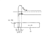
Below, with reference to accompanying drawing embodiments of the invention are described.Fig. 1 is a profile of representing the light generating device of the embodiment of the invention 1 by manufacturing process.
As the crystal semiconductor substrate, single crystal silicon substrate, polycrystal silicon substrate etc. are arranged, as present embodiment, used thickness is 300 microns, the resistivity single crystal silicon substrate 11 less than 5 Ω cm.Use alkaline solutions such as sodium hydroxide solution, potassium hydroxide solution to implement anisotropic etching, carry out concavo-convexization at the surperficial back side of this single crystal silicon substrate 11.
Clean single crystal silicon substrate 11 is put into vacuum chamber, is heated to be lower than 200 ℃, removes attached to the moisture on the substrate surface as far as possible.In the present embodiment, substrate temperature is heated to 170 ℃.
Then, import hydrogen (H
2), carry out plasma discharge, the cleaning base plate surface.This processing has the effect that reduces substrate surface carbon amount as can be known.
In the present embodiment, when hydrogen plasma is handled, import hydrogen (H
2) and diborane gas (B
2H
6), decompose boron (B), and make boron absorption from the teeth outwards, import boron (with reference to Fig. 1 (a)) to the single crystal silicon substrate surface.The condition of this moment is as shown in table 1.
Afterwards, import silane gas (SiH
4) and as the hydrogen (H of diluent gas
2), substrate is remained on 170 ℃, by plasma CVD method, form unadulterated i type amorphous silicon layer 12.Then, import silane gas (SiH
4), as the hydrogen (H of diluent gas
2) and as the diborane gas (B of impurity gas
2H
6), forming p type amorphous silicon layer 13 successively by plasma CVD method, and form pn knot (with reference to Fig. 1 (b)), the condition of this moment is as shown in table 1.
Then, at the hydrogenated amorphous attitude silicon thin film of the same formation of the rear side of said n type single crystal silicon substrate 11.At first, n type single crystal silicon substrate 11 is put into vacuum chamber, be heated to below 200 ℃.In the present embodiment, substrate is heated to 170 ℃.Then, at hydrogen (H
2) in carry out plasma discharge.Afterwards, import silane gas (SiH
4) and as the hydrogen (H of diluent gas
2), substrate is remained on 170 ℃, by plasma CVD method, form unadulterated i type amorphous silicon layer 14.Then, import silane gas (SiH
4), as the hydrogen (H of diluent gas
2) and as the phosphine gas (PH of impurity gas
3), forming n type amorphous silicon layer 15 successively by plasma CVD method, and form BSF structure (with reference to Fig. 1 (c)) in the rear side of n type single crystal silicon substrate 11, the formation condition of this moment is as shown in table 1.
In addition, form tin indium oxide (ITO) film 16 as the face side electrode, form silver electrode 18 as collector electrode by the wire mark method by sputtering method.In addition, form ITO film 17 as the rear side electrode, form silver electrode 19 as collector electrode, finish light generating device (with reference to Fig. 1 (d)) by the wire mark method by sputtering method.
In the above-described embodiments, side forms so-called BSF structure overleaf, but also can not form the BSF structure.When forming the BSF structure, for the order of making amorphous silicon layer, as mentioned above, both can begin to form from face side (p type side), also can begin to form from rear side (n type side).
The concrete formation condition of above-mentioned light generating device is as shown in table 1.
Table 1

Fig. 2 represents the band structure of semiconductor junction of the present invention.Among Fig. 2, solid line is represented band structure of the present invention, and dotted line is illustrated in the existing band structure that does not import diborane in the hydrogen plasma processing.
The light generating device that is formed by said method forms essence on n type single crystal silicon substrate 11 is the amorphous silicon layer 12 of i type and forms n type amorphous silicon layer 13 thereon, forms ITO film 16 again on n type amorphous silicon layer 13.In addition, in the interface of substrate 11 and i type amorphous silicon layer 12, import the required boron of excessive compensation i type amorphous silicon layer.
As shown in Figure 2, by in the interface of single crystallization base plate 11 and i type amorphous silicon layer 12, importing boron greater than compensation amorphous silicon layer aequum, the amorphous silicon layer 12 of near interface becomes extremely weak p type, simultaneously, can be confined to the electric field grow in the single crystal silicon substrate 11 of near interface.Therefore, near electronics and the hole that exists the separating interface is reduced in the probability that the interface is coupled again effectively.In addition, the potential barrier of the not coupling part of the frequency band of valence band in the interface diminishes relatively, and it is easy that charge carrier moves transfiguration.As a result, can improve open circuit voltage in the characteristic of solar cell.
At this moment, though the electric field strength that exists in the i type amorphous silicon layer dies down, can obtain making the charge carrier in the amorphous layer to move the very easy electric field that becomes thus.
In addition, if boron excess is provided, then the electric field strength of i type amorphous silicon layer 12 diminishes, the increase that is coupled again of charge carrier in this part, if further increase, then pile up p type amorphous silicon layer equivalence substantially and directly on n type single crystal silicon substrate, the boron that exists by surplus is coupled again, and characteristic of solar cell reduces.
As light generating device of the present invention, under the formation condition shown in the above-mentioned table 1, make light generating device.So the output characteristic of the light generating device of making is as shown in table 2.Here, use in above-mentioned hydrogen plasma is handled, do not import diborane gas situation as a comparative example.These samples form the BSF layer of rear side simultaneously.
Table 2
| Voc(V) | Isc(A) | F.F. | Pmax(W) | |
| Do not import B 2H 6 | 0.670 | 3.72 | 0.75 | 1.87 |
| Import B 2H 6 | 0.692 | 3.70 | 0.76 | 1.95 |
As known from Table 2, in hydrogen plasma is handled, import diborane gas, find that open circuit voltage improves, and confirms validity of the present invention.
The thickness of the amorphous layer of table 1 illustrated embodiment, i type amorphous silicon layer is about 7nm, p type layer is about 5nm, because can not observe in the resolution capability (10nm to 20nm) of depth direction, be the result that 160nm, p type layer are about 8nm along the impurity profile of depth direction so observe i type amorphous silicon layer thickness shown in Fig. 3 by existing secondary ion mass spectrometry instrument.
Here, analyze, measure the boron atomic density at interface from the amorphous silicon layer side along depth direction, by obtain the volumetric concentration of boron (B) at the depth direction integration by SIMS (secondary ion mass spectroscopy).In addition, calculate the surface density at interface according to the bulk density of (2nm-3nm) before and after the interface of depth direction, as interface boron atomic density.
Among the figure, dotted line is the interface location according to each layer of formation of contour prediction.Have about 6 * 10 in the substrate interface
11Cm
-2The boron (B) of interface boron atomic density amount.Reducing, reduce any from the dullness of the boron amount of substrate interface in substrate and all be more prone to gently than Gaussian Profile from the dullness of the boron amount of p type amorphous silicon surface in intrinsic (i type) amorphous silicon layer, is owing to squeezing into effect when the sputter the sims analysis from experience as can be known.
Therefore, think that in fact boron concentration sharply reduces on each interface, in substrate, do not spread basically from i type amorphous silicon layer and substrate interface.Under the situation of observing actual solar cell, also, think to have the measurement result of the profile of boron (B) profile that is similar to Fig. 3 by using depth direction resolution high (1nm-2nm) to hang down assay methods such as quickening SIMS.
Below, embodiments of the invention 2 are described.
The n type single crystal silicon substrate of having cleaned is put into vacuum chamber, is heated to be lower than 200 ℃, removes attached to the moisture on the substrate surface as far as possible.In the present embodiment, substrate is heated to 170 ℃.
Then, import hydrogen (H
2), carry out plasma discharge, the cleaning base plate surface.Afterwards, import hydrogen (H
2), diborane gas (B
2H
6), silane gas (SiH
4), carry out plasma discharge, substrate surface pile up about 1nm as thin as a wafer and first amorphous silicon layer that imports low concentration p type impurity 1., near interface importing boron.Afterwards, the same with embodiment 1, form successively i type amorphous silicon layer 2., p type amorphous silicon layer, finish pn knot.In addition, form tin indium oxide (ITO) film as the face side electrode, form silver electrode as collector electrode by the wire mark method by sputtering method.
Under the formation condition shown in the table 3, form the light generating device of the embodiment of the invention 2.
Table 3

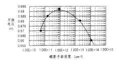
Fig. 4 represents that the open circuit voltage characteristic imports the diborane gas (B that trace is made at the near interface of substrate that is formed by condition shown in the above-mentioned table 3 and amorphous silicon layer relatively
2H
6) after the performance plot that changes of the boron import volume of the type of p as thin as a wafer amorphous silicon layer.
As shown in Figure 4, with do not import diborane gas (B
2H
6) situation compare, the open circuit voltage stage rises, and if doping is more for a long time, open circuit voltage turns to and reduces tendency.Compare with situation about not importing, with the boron atomic plane density of boron import volume, 1 * 10 as the interface
11Cm
-2More than 5 * 10
13Cm
-2Can improve open circuit voltage under the following scope.According to Fig. 4, preferably control diborane gas (B
2H
6) amount, make interface boron atomic plane density in the interface that imports substrate and amorphous silicon layer 1 * 10
11Cm
-2More than 5 * 10
13Cm
-2In the following scope.
Below, embodiments of the invention 3 are described.
The n type single crystal silicon substrate of having cleaned is put into vacuum chamber, is heated to be lower than 200 ℃, removes attached to the moisture on the substrate surface as far as possible.In the present embodiment, substrate is heated to 170 ℃.
Then, import hydrogen (H
2), carry out plasma discharge, the cleaning base plate surface.Afterwards, import hydrogen (H
2), diborane gas (B
2H
6), substrate is exposed to the open air in above-mentioned gas.Diborane gas (B
2H
6) decompose at the substrate surface of heating, be adsorbed on the substrate surface, can import boron to the interface.As exposing condition to the open air, substrate temperature is 170 ℃, 2% diborane gas (B
2H
6) be 100sccm, pressure is 40Pa, the time is 1-600 second.
Afterwards, the same with embodiment 1, form i type amorphous silicon layer, p type amorphous silicon layer successively, finish the pn knot.In addition, form tin indium oxide (ITO) film as the face side electrode, form silver electrode as collector electrode by the wire mark method by sputtering method.
Also the same in the case with embodiment 1, confirm that open circuit voltage improves.In addition, the characteristic difference under the condition that do not expose to the open air basically changes has or not that to expose the variation that causes to the open air big.
As mentioned above, for the pn knot that constitutes by crystallization series silicon and amorphous silicon, by being mingled with boron in right amount as the crystallization series silicon of substrate and the near interface of amorphous silicon film, the charge carrier that can suppress at the interface is coupled again, improves coupled characteristic.Solar cell for using this coupling can improve open circuit voltage.
Illustrated among the foregoing description 1-3 and improved the pn junction characteristic, made the BFS effect good among the embodiment 4.The following describes embodiment 4.
Below, with reference to accompanying drawing embodiments of the invention are described.Fig. 5 is a profile of representing the light generating device of the embodiment of the invention 4 by manufacturing process.
As the crystal semiconductor substrate, single crystal silicon substrate, polycrystal silicon substrate etc. are arranged, the same with embodiment 1 as embodiment 4, used thickness is 300 microns, the resistivity single crystal silicon substrate 11 less than 5 Ω cm.Use alkaline solutions such as sodium hydroxide solution, potassium hydroxide solution that anisotropic etching is implemented at the surperficial back side of this single crystal silicon substrate 11, carry out concavo-convexization.
Then, import hydrogen (H
2), carry out plasma discharge, the cleaning base plate surface.
In embodiment 4, when hydrogen plasma is handled, import hydrogen (H
2) and phosphine gas (PH
3), divide phosphorus decomposing (P), and make phosphorus absorption from the teeth outwards, import phosphorus (with reference to Fig. 5 (a)) to the back side of single crystal silicon substrate 11.The condition of this moment is as shown in table 4.
Afterwards, import silane gas (SiH
4) and as the hydrogen (H of diluent gas
2), substrate is remained on 170 ℃, by plasma CVD method, form unadulterated i type amorphous silicon layer 14.Then, import silane gas (SiH
4), as the hydrogen (H of diluent gas
2) and as the phosphine gas (PH of impurity gas
3), forming n type amorphous silicon layer 15 successively by plasma CVD method, and form BSF structure (with reference to Fig. 5 (b)) in the rear side of n type single crystal silicon substrate 11, the condition of this moment is as shown in table 4.
Then, at the hydrogenated amorphous attitude silicon thin film of the same formation of the rear side of said n type single crystal silicon substrate 11.At first, n type single crystal silicon substrate 11 is put into vacuum chamber, be heated to below 200 ℃.In embodiment 4, substrate is heated to 170 ℃.Then, at hydrogen (H
2) in carry out plasma discharge.Afterwards, import silane gas (SiH
4) and as the hydrogen (H of diluent gas
2), substrate is remained on 170 ℃, forming essence by plasma CVD method is i type amorphous silicon layer 12.Then, import silane gas (SiH
4), as the hydrogen (H of diluent gas
2) and as the diborane gas (B of impurity gas
2H
6), forming p type amorphous silicon layer 13 successively by plasma CVD method, and form pn knot (with reference to Fig. 5 (c)), the condition of this moment is as shown in table 4.
In addition, form ITO film 16 as the face side electrode, form silver electrode 18 as collector electrode by the wire mark method by sputtering method.In addition, form ITO film 17 as the rear side electrode, form silver electrode 19 as collector electrode, finish light generating device (with reference to Fig. 5 (d)) by the wire mark method by sputtering method.
The concrete formation condition of above-mentioned light generating device is as shown in table 4.
Table 4

Then, at the hydrogen and the hydrogen phosphide (PH of single crystal silicon substrate 11 rear side
3) the plasma treatment of mist in, make PH
3The flow change in concentration of gas, the output characteristic result who measures when changing interface phosphorus atoms density is as shown in table 5.As shown in Figure 6, interface phosphorus atoms concentration is measured along depth direction from amorphous silicon layer 16 sides by sims analysis, obtains the volumetric concentration of phosphorus (P) behind the depth direction integration.In addition, according to the zone that adds shade among Fig. 6, be that the bulk density of (2nm-3nm) is calculated the surface density at interface before and after the interface of depth direction, as interface phosphorus atoms concentration.
Table 5
| P density (cm -2) | Voc(V) | Isc(A) | FF | Pmax(W) | |
| Do not import PH 3 | 9.20E+10 | 0.677 | 3.730 | 0.751 | 1.896 |
| Import PH 3a | 5.00E+11 | 0.690 | 3.725 | 0.771 | 1.982 |
| Import PH 3b | 7.00E+12 | 0.710 | 3.720 | 0.766 | 2.023 |
| Import PH 3c | 2.00E+14 | 0.693 | 3.721 | 0.762 | 1.965 |
| Import PH 3d | 5.00E+15 | 0.665 | 3.710 | 0.745 | 1.845 |
As known from Table 5, in the plasma treatment of single crystal silicon substrate 11 rear side, and do not import phosphine gas (PH
3) comparative example compare, according to importing phosphine gas (PH
3) the embodiment of the invention 4 improved open circuit voltage and fill factor (F.F.) as can be known.By importing phosphorus to the interface, can relax the influence of band bending, improve electron stream.
Fig. 7 illustrates to measure and imports phosphine gas (PH
3) after carry out the light generating device under the situation of plasma treatment output (unit output) (Pmax) with the result of the relation of the interface phosphorus atoms density of rear side.
As can be seen from Figure 7, if phosphorus atoms density in interface is 1 * 10
11Cm
-2More than 5 * 10
14Cm
-2Below, then unit output surpasses 1.900W, the result who obtains.Thus, in the plasma treatment of the rear side of single crystal silicon substrate 11, control imports phosphine gas (PH
3) flow, make interface phosphorus atoms density 1 * 10
11Cm
-2More than 5 * 10
14Cm
-2Below.
Below, embodiments of the invention 5 are described.
N type single crystal silicon substrate after cleaning is put into vacuum chamber, is heated to be lower than 200 ℃, removes attached to the moisture on the substrate surface as far as possible.In the present embodiment, substrate is heated to 170 ℃.
Then, import hydrogen (H
2), carry out plasma discharge, the cleaning base plate surface.Afterwards, import hydrogen (H
2), phosphine gas (PH
3), silane gas (SiH
4), carry out plasma discharge, substrate surface pile up about 1nm as thin as a wafer and the 4th amorphous silicon layer that imports low concentration n type impurity 4., near interface importing phosphorus.Afterwards, the same with embodiment 4, form successively i type amorphous silicon layer 5., n type amorphous silicon layer, finish the BSF structure.In addition, also the same in n type single crystal silicon substrate surface side with embodiment 4, form i type amorphous silicon layer, p type amorphous silicon layer successively, and form the pn knot.Form tin indium oxide (ITO) film as face side and rear side electrode by sputtering method, form silver electrode as collector electrode by the wire mark method.
Under condition shown in the table 6, form the light generating device of the embodiment of the invention 5.
Table 6

At this moment, the same with embodiment 4, confirm that open circuit voltage improves.
Below, embodiments of the invention 6 are described.
The n type single crystal silicon substrate of having cleaned is put into vacuum chamber, is heated to be lower than 200 ℃, removes attached to the moisture on the substrate surface as far as possible.In the present embodiment, substrate is heated to 170 ℃.
Then, import hydrogen (H
2), carry out plasma discharge, the cleaning base plate surface.Afterwards, import hydrogen (H
2), phosphine gas (PH
3), substrate is exposed to the open air in above-mentioned gas.Phosphine gas (PH
3) decompose at the substrate surface of heating, be adsorbed on the substrate surface, can import boron to the interface.As exposing condition to the open air, substrate temperature is 170 ℃, 1% phosphine gas (PH
3) be 100sccm, pressure is 40Pa, the time is 1-600 second.
Afterwards, the same with embodiment 4, form i type amorphous silicon layer, n type amorphous silicon layer successively, finish the BSF structure.In addition, also the same in n type single crystal silicon substrate surface side with embodiment 4, form amorphous silicon layer, the p type amorphous silicon layer that is essentially the i type successively, and form the pn knot.Form tin indium oxide (ITO) film as face side and rear side electrode by sputtering method, form silver electrode as collector electrode by the wire mark method.
Also the same in the case with embodiment 4, confirm that open circuit voltage improves.In addition, characteristic does not have difference substantially under the condition that exposes to the open air changes, and has or not that to expose the variation that causes to the open air big.
In addition, the various embodiments described above are used n type substrate, but much less, substrate is being made as the p type, make the amorphous silicon layer of amorphous silicon layer, n type of i type and ITO film, silver electrode in the table side, also just the same processing when dorsal part is made the amorphous silicon layer of amorphous silicon layer, p type of i type and ITO film, silver electrode.In addition, as the crystallization series substrate, under the situation of using n type, p type polycrystal silicon substrate to make, also can obtain same result.
In addition, in the various embodiments described above,, also can in two interfaces at the surperficial back side, import impurity though in a certain side in interface of the face side interface of substrate or rear side, have a conductivity type or other conductive-type impurities.For example, by combination embodiment 1 and embodiment 4, import each self-corresponding impurity in the interface at the surperficial back side of substrate, both sides' combination of effects can expect further to improve the characteristic of solar cell.
In addition, in the above-described embodiments, use amorphous silicon film as amorphous semiconductor film, but equally also can use the micro-crystallization silicon thin film.In addition, in the above-described embodiments, use silicon has been described, but under the situation of using germanium, also can have expected same effect as semi-conductive situation.
In addition, in the above-described embodiments, use phosphorus as the situation that belongs to the atom of periodic table 5B family, use other atoms that belong to periodic table 5B family, for example arsenic element (As), antimony (Sb) etc. also can expect same effect though described.In addition, use boron as the situation that belongs to the atom of periodic table 3B family, use other atoms that belong to periodic table 3B family, for example aluminium element (Al) etc. also can expect same effect though described.
Claims (5)
1, a kind of light generating device, it is characterized in that: the amorphous silicon film that on a conductivity type crystal semiconductor, forms intrinsic, and a conductivity type or other conductivity type amorphous semiconductor films be set on the amorphous silicon film of described intrinsic, wherein, on the interface that the amorphous silicon film of above-mentioned crystal semiconductor and described intrinsic forms, import a conductivity type or other conductive-type impurities greater than compensation amorphous silicon film aequum.
2, light generating device according to claim 1, it is characterized in that: a described conductivity type is the n-type, described other conductivity types are p-types, described crystal semiconductor is a n-type crystallization series silicon, amorphous semiconductor film is the amorphous silicon film, described n-type impurity is the atom that belongs to periodic table 5B family, and its interface foreign atom surface density is 1 * 10
11Cm
-2More than 5 * 10
14Cm
-2Below.
3, light generating device according to claim 1 and 2, it is characterized in that: a described conductivity type is the n-type, described other conductivity types are p-types, described crystal semiconductor is a n-type crystallization series silicon, amorphous semiconductor film is the amorphous silicon film, described p-type impurity is the atom that belongs to periodic table 3B family, and its interface foreign atom surface density is 1 * 10
11Cm
-2More than 5 * 10
13Cm
-2Below.
4, light generating device according to claim 1, it is characterized in that: a described conductivity type is the p-type, described other conductivity types are n-types, described crystal semiconductor is a p-type crystallization series silicon, amorphous semiconductor film is the amorphous silicon film, described p-type impurity is the atom that belongs to periodic table 3B family, and its interface foreign atom surface density is 1 * 10
11Cm
-2More than 5 * 10
13Cm
-2Below.
5, according to claim 1 or 4 described light generating devices, it is characterized in that: a described conductivity type is the p-type, described other conductivity types are n-types, described crystal semiconductor is a p-type crystallization series silicon, amorphous semiconductor film is the amorphous silicon film, described n-type impurity is the atom that belongs to periodic table 5B family, and its interface foreign atom surface density is 1 * 10
11Cm
-2More than 5 * 10
14Cm
-2Below.
Applications Claiming Priority (6)
| Application Number | Priority Date | Filing Date | Title |
|---|---|---|---|
| JP2001365265 | 2001-11-29 | ||
| JP2001365265 | 2001-11-29 | ||
| JP2002054767 | 2002-02-28 | ||
| JP2002054767 | 2002-02-28 | ||
| JP2002327345 | 2002-11-11 | ||
| JP2002327345A JP3902534B2 (en) | 2001-11-29 | 2002-11-11 | Photovoltaic device and manufacturing method thereof |
Publications (2)
| Publication Number | Publication Date |
|---|---|
| CN1445865A CN1445865A (en) | 2003-10-01 |
| CN100449792C true CN100449792C (en) | 2009-01-07 |
Family
ID=27347889
Family Applications (1)
| Application Number | Title | Priority Date | Filing Date |
|---|---|---|---|
| CNB02157586XA Expired - Lifetime CN100449792C (en) | 2001-11-29 | 2002-11-29 | Light generating device and manufacturing method thereof |
Country Status (4)
| Country | Link |
|---|---|
| US (1) | US6878921B2 (en) |
| EP (1) | EP1320134B1 (en) |
| JP (1) | JP3902534B2 (en) |
| CN (1) | CN100449792C (en) |
Families Citing this family (60)
| Publication number | Priority date | Publication date | Assignee | Title |
|---|---|---|---|---|
| US20050252544A1 (en) * | 2004-05-11 | 2005-11-17 | Ajeet Rohatgi | Silicon solar cells and methods of fabrication |
| EP1643564B1 (en) * | 2004-09-29 | 2019-01-16 | Panasonic Intellectual Property Management Co., Ltd. | Photovoltaic device |
| CN100334744C (en) * | 2005-04-21 | 2007-08-29 | 中电电气(南京)光伏有限公司 | Silicon solar battery structure and making method |
| KR100880946B1 (en) * | 2006-07-03 | 2009-02-04 | 엘지전자 주식회사 | Solar Cell and Manufacturing Method thereof |
| DE102006042617B4 (en) | 2006-09-05 | 2010-04-08 | Q-Cells Se | Method for generating local contacts |
| FR2906406B1 (en) * | 2006-09-26 | 2008-12-19 | Commissariat Energie Atomique | PROCESS FOR PRODUCING A PHOTOVOLTAIC CELL WITH REAR-SIDE HETEROJUNCTION |
| US20080179762A1 (en) * | 2007-01-25 | 2008-07-31 | Au Optronics Corporation | Layered structure with laser-induced aggregation silicon nano-dots in a silicon-rich dielectric layer, and applications of the same |
| US9577137B2 (en) * | 2007-01-25 | 2017-02-21 | Au Optronics Corporation | Photovoltaic cells with multi-band gap and applications in a low temperature polycrystalline silicon thin film transistor panel |
| US7960644B2 (en) * | 2007-11-09 | 2011-06-14 | Sunpreme, Ltd. | Low-cost multi-junction solar cells and methods for their production |
| JP5572307B2 (en) * | 2007-12-28 | 2014-08-13 | 株式会社半導体エネルギー研究所 | Method for manufacturing photoelectric conversion device |
| KR101028085B1 (en) * | 2008-02-19 | 2011-04-08 | 엘지전자 주식회사 | Etching method of a non-symmetric wafer, solar cell comprising the non-symmetrically etched wafer, and fabricating method thereof |
| US8076175B2 (en) * | 2008-02-25 | 2011-12-13 | Suniva, Inc. | Method for making solar cell having crystalline silicon P-N homojunction and amorphous silicon heterojunctions for surface passivation |
| JP2009200419A (en) * | 2008-02-25 | 2009-09-03 | Seiko Epson Corp | Method for manufacturing solar cell manufacturing method |
| US20090211623A1 (en) * | 2008-02-25 | 2009-08-27 | Suniva, Inc. | Solar module with solar cell having crystalline silicon p-n homojunction and amorphous silicon heterojunctions for surface passivation |
| DE102008030693A1 (en) * | 2008-07-01 | 2010-01-14 | Institut Für Solarenergieforschung Gmbh | Heterojunction solar cell with absorber with integrated doping profile |
| FR2936905B1 (en) | 2008-10-02 | 2010-10-29 | Commissariat Energie Atomique | TWO - DOPING HETEROJUNCTION PHOTOVOLTAIC CELL AND METHOD OF MANUFACTURING THE SAME. |
| US8796066B2 (en) * | 2008-11-07 | 2014-08-05 | Sunpreme, Inc. | Low-cost solar cells and methods for fabricating low cost substrates for solar cells |
| US7951640B2 (en) * | 2008-11-07 | 2011-05-31 | Sunpreme, Ltd. | Low-cost multi-junction solar cells and methods for their production |
| US7858427B2 (en) * | 2009-03-03 | 2010-12-28 | Applied Materials, Inc. | Crystalline silicon solar cells on low purity substrate |
| US9130074B2 (en) * | 2009-04-21 | 2015-09-08 | Tetrasun, Inc. | High-efficiency solar cell structures and methods of manufacture |
| US20100300507A1 (en) * | 2009-06-02 | 2010-12-02 | Sierra Solar Power, Inc. | High efficiency low cost crystalline-si thin film solar module |
| WO2011030741A1 (en) * | 2009-09-08 | 2011-03-17 | 株式会社カネカ | Transparent electrode and crystalline silicon solar cell |
| US9012766B2 (en) | 2009-11-12 | 2015-04-21 | Silevo, Inc. | Aluminum grid as backside conductor on epitaxial silicon thin film solar cells |
| TW201121066A (en) * | 2009-12-14 | 2011-06-16 | Ind Tech Res Inst | Bificial solar cell |
| TWI408822B (en) * | 2009-12-31 | 2013-09-11 | Lu Sheng Hong | Thin silicon solar cell and its manufacturing method |
| US9214576B2 (en) | 2010-06-09 | 2015-12-15 | Solarcity Corporation | Transparent conducting oxide for photovoltaic devices |
| CN102315312B (en) * | 2010-07-09 | 2013-11-13 | 国立清华大学 | Manufacturing process of silicon heterojunction solar battery |
| US9773928B2 (en) | 2010-09-10 | 2017-09-26 | Tesla, Inc. | Solar cell with electroplated metal grid |
| US9800053B2 (en) | 2010-10-08 | 2017-10-24 | Tesla, Inc. | Solar panels with integrated cell-level MPPT devices |
| TWI455329B (en) * | 2010-10-26 | 2014-10-01 | Au Optronics Corp | Solar cell and method of making the same |
| US8895435B2 (en) * | 2011-01-31 | 2014-11-25 | United Microelectronics Corp. | Polysilicon layer and method of forming the same |
| US9054256B2 (en) | 2011-06-02 | 2015-06-09 | Solarcity Corporation | Tunneling-junction solar cell with copper grid for concentrated photovoltaic application |
| JP5927027B2 (en) * | 2011-10-05 | 2016-05-25 | 株式会社半導体エネルギー研究所 | Photoelectric conversion device |
| WO2013128628A1 (en) * | 2012-03-02 | 2013-09-06 | 三洋電機株式会社 | Photovoltaic device |
| JPWO2014050304A1 (en) * | 2012-09-27 | 2016-08-22 | パナソニックIpマネジメント株式会社 | Photoelectric conversion element and manufacturing method thereof |
| WO2014055781A1 (en) | 2012-10-04 | 2014-04-10 | Silevo, Inc. | Photovoltaic devices with electroplated metal grids |
| US9865754B2 (en) | 2012-10-10 | 2018-01-09 | Tesla, Inc. | Hole collectors for silicon photovoltaic cells |
| US9306106B2 (en) * | 2012-12-18 | 2016-04-05 | International Business Machines Corporation | Monolithic integration of heterojunction solar cells |
| US9281436B2 (en) | 2012-12-28 | 2016-03-08 | Solarcity Corporation | Radio-frequency sputtering system with rotary target for fabricating solar cells |
| US9412884B2 (en) | 2013-01-11 | 2016-08-09 | Solarcity Corporation | Module fabrication of solar cells with low resistivity electrodes |
| US10074755B2 (en) | 2013-01-11 | 2018-09-11 | Tesla, Inc. | High efficiency solar panel |
| US9219174B2 (en) | 2013-01-11 | 2015-12-22 | Solarcity Corporation | Module fabrication of solar cells with low resistivity electrodes |
| US20140196773A1 (en) * | 2013-01-11 | 2014-07-17 | International Business Machines Corporation | Multi-junction iii-v solar cell |
| US9624595B2 (en) | 2013-05-24 | 2017-04-18 | Solarcity Corporation | Electroplating apparatus with improved throughput |
| TWI469380B (en) * | 2013-11-08 | 2015-01-11 | Ind Tech Res Inst | Hit solar cell structure |
| US10309012B2 (en) | 2014-07-03 | 2019-06-04 | Tesla, Inc. | Wafer carrier for reducing contamination from carbon particles and outgassing |
| US9899546B2 (en) | 2014-12-05 | 2018-02-20 | Tesla, Inc. | Photovoltaic cells with electrodes adapted to house conductive paste |
| US9947822B2 (en) | 2015-02-02 | 2018-04-17 | Tesla, Inc. | Bifacial photovoltaic module using heterojunction solar cells |
| DE102015101966B4 (en) * | 2015-02-11 | 2021-07-08 | Infineon Technologies Austria Ag | Method for producing a semiconductor component with Schottky contact and semiconductor component |
| US9761744B2 (en) | 2015-10-22 | 2017-09-12 | Tesla, Inc. | System and method for manufacturing photovoltaic structures with a metal seed layer |
| US9842956B2 (en) | 2015-12-21 | 2017-12-12 | Tesla, Inc. | System and method for mass-production of high-efficiency photovoltaic structures |
| JP6609324B2 (en) * | 2015-12-24 | 2019-11-20 | 株式会社カネカ | Method for manufacturing photoelectric conversion device |
| US9496429B1 (en) | 2015-12-30 | 2016-11-15 | Solarcity Corporation | System and method for tin plating metal electrodes |
| JP6785427B2 (en) | 2016-02-01 | 2020-11-18 | パナソニックIpマネジメント株式会社 | Solar cell elements and solar cell modules |
| US10115838B2 (en) | 2016-04-19 | 2018-10-30 | Tesla, Inc. | Photovoltaic structures with interlocking busbars |
| JP2016219854A (en) * | 2016-09-30 | 2016-12-22 | パナソニックIpマネジメント株式会社 | Photovoltaic device and method for manufacturing photoelectric conversion device |
| CN106531835B (en) * | 2016-10-31 | 2018-03-30 | 新奥光伏能源有限公司 | A kind of silicon heterogenous solar cell and solar cell module |
| CN107170850A (en) * | 2017-05-25 | 2017-09-15 | 君泰创新(北京)科技有限公司 | The preparation method and heterojunction solar battery of a kind of heterojunction solar battery |
| US10672919B2 (en) | 2017-09-19 | 2020-06-02 | Tesla, Inc. | Moisture-resistant solar cells for solar roof tiles |
| US11190128B2 (en) | 2018-02-27 | 2021-11-30 | Tesla, Inc. | Parallel-connected solar roof tile modules |
Citations (2)
| Publication number | Priority date | Publication date | Assignee | Title |
|---|---|---|---|---|
| CN1043040A (en) * | 1985-11-05 | 1990-06-13 | 钟渊化学工业株式会社 | Semiconductor device |
| US5213628A (en) * | 1990-09-20 | 1993-05-25 | Sanyo Electric Co., Ltd. | Photovoltaic device |
Family Cites Families (5)
| Publication number | Priority date | Publication date | Assignee | Title |
|---|---|---|---|---|
| US4217148A (en) * | 1979-06-18 | 1980-08-12 | Rca Corporation | Compensated amorphous silicon solar cell |
| JPH0795603B2 (en) | 1990-09-20 | 1995-10-11 | 三洋電機株式会社 | Photovoltaic device |
| JPH0794768A (en) * | 1993-09-22 | 1995-04-07 | Sanyo Electric Co Ltd | Photovoltaic device |
| US5769963A (en) * | 1995-08-31 | 1998-06-23 | Canon Kabushiki Kaisha | Photovoltaic device |
| JP2001189478A (en) * | 1999-12-28 | 2001-07-10 | Sanyo Electric Co Ltd | Semiconductor element and manufacturing method therefor |
-
2002
- 2002-11-11 JP JP2002327345A patent/JP3902534B2/en not_active Expired - Lifetime
- 2002-11-27 US US10/305,262 patent/US6878921B2/en not_active Expired - Lifetime
- 2002-11-29 EP EP02026704.3A patent/EP1320134B1/en not_active Expired - Lifetime
- 2002-11-29 CN CNB02157586XA patent/CN100449792C/en not_active Expired - Lifetime
Patent Citations (2)
| Publication number | Priority date | Publication date | Assignee | Title |
|---|---|---|---|---|
| CN1043040A (en) * | 1985-11-05 | 1990-06-13 | 钟渊化学工业株式会社 | Semiconductor device |
| US5213628A (en) * | 1990-09-20 | 1993-05-25 | Sanyo Electric Co., Ltd. | Photovoltaic device |
Also Published As
| Publication number | Publication date |
|---|---|
| EP1320134B1 (en) | 2015-09-09 |
| EP1320134A2 (en) | 2003-06-18 |
| CN1445865A (en) | 2003-10-01 |
| EP1320134A3 (en) | 2007-07-04 |
| US20030168578A1 (en) | 2003-09-11 |
| JP2003324209A (en) | 2003-11-14 |
| JP3902534B2 (en) | 2007-04-11 |
| US6878921B2 (en) | 2005-04-12 |
Similar Documents
| Publication | Publication Date | Title |
|---|---|---|
| CN100449792C (en) | Light generating device and manufacturing method thereof | |
| JP4070483B2 (en) | Photovoltaic device and manufacturing method thereof | |
| EP1300889B1 (en) | Photovoltaic Device | |
| US10763386B2 (en) | Heterostructure germanium tandem junction solar cell | |
| CN103718276B (en) | Make the method for amorphous silicon hydride and amorphous silane alloy stabilisation | |
| US9105770B2 (en) | Shallow junction photovoltaic devices | |
| DE102006042617A1 (en) | Local hetero-contact producing device for high-power solar cell, has surface passivated-layer of semiconductor material formed by plasma etching, where foil serves as masking for separation processes of hetero contacts | |
| EP2978028A1 (en) | Photovoltaic device | |
| US20140020742A1 (en) | Photoelectric conversion device and method for producing photoelectric conversion device | |
| US20130052774A1 (en) | Method for surface-treating semiconductor substrate, semiconductor substrate, and method for producing solar battery | |
| US10134928B2 (en) | Photoelectric conversion element and solar cell module provided with same | |
| AU2014239465B2 (en) | Photovoltaic element and manufacturing method therefor | |
| US20120174972A1 (en) | Transparent conductive film and a device with the same | |
| CN104145344A (en) | Photovoltaic device | |
| DE102012104140A1 (en) | Improved emitter structure and method of making a silicon solar cell with heterojunction | |
| JP2003282458A (en) | Semiconductor device and method of manufacturing the same | |
| JP4159390B2 (en) | Photovoltaic element and manufacturing method thereof | |
| CN111742416B (en) | Method for manufacturing solar cell | |
| CN111727508B (en) | Method for manufacturing solar cell | |
| WO2019004126A1 (en) | Method for manufacturing photoelectric conversion device | |
| Magramene et al. | Passivation of grain boundary electronic activity in polycrystalline silicon thin films by heat treatment and hydrogenation | |
| JP2002343990A (en) | Photovoltaic element | |
| JPH08116080A (en) | Thin film solar cell and its manufacture |
Legal Events
| Date | Code | Title | Description |
|---|---|---|---|
| C06 | Publication | ||
| PB01 | Publication | ||
| C10 | Entry into substantive examination | ||
| SE01 | Entry into force of request for substantive examination | ||
| C14 | Grant of patent or utility model | ||
| GR01 | Patent grant | ||
| CX01 | Expiry of patent term |
Granted publication date: 20090107 |
|
| CX01 | Expiry of patent term |