CN100423064C - Displaying device and its mfg. method - Google Patents
Displaying device and its mfg. method Download PDFInfo
- Publication number
- CN100423064C CN100423064C CNB01108958XA CN01108958A CN100423064C CN 100423064 C CN100423064 C CN 100423064C CN B01108958X A CNB01108958X A CN B01108958XA CN 01108958 A CN01108958 A CN 01108958A CN 100423064 C CN100423064 C CN 100423064C
- Authority
- CN
- China
- Prior art keywords
- line
- display device
- source electrode
- film transistor
- film
- Prior art date
- Legal status (The legal status is an assumption and is not a legal conclusion. Google has not performed a legal analysis and makes no representation as to the accuracy of the status listed.)
- Expired - Fee Related
Links
Images


Classifications
-
- H—ELECTRICITY
- H10—SEMICONDUCTOR DEVICES; ELECTRIC SOLID-STATE DEVICES NOT OTHERWISE PROVIDED FOR
- H10K—ORGANIC ELECTRIC SOLID-STATE DEVICES
- H10K50/00—Organic light-emitting devices
- H10K50/80—Constructional details
- H10K50/84—Passivation; Containers; Encapsulations
- H10K50/844—Encapsulations
-
- G—PHYSICS
- G02—OPTICS
- G02F—OPTICAL DEVICES OR ARRANGEMENTS FOR THE CONTROL OF LIGHT BY MODIFICATION OF THE OPTICAL PROPERTIES OF THE MEDIA OF THE ELEMENTS INVOLVED THEREIN; NON-LINEAR OPTICS; FREQUENCY-CHANGING OF LIGHT; OPTICAL LOGIC ELEMENTS; OPTICAL ANALOGUE/DIGITAL CONVERTERS
- G02F1/00—Devices or arrangements for the control of the intensity, colour, phase, polarisation or direction of light arriving from an independent light source, e.g. switching, gating or modulating; Non-linear optics
- G02F1/01—Devices or arrangements for the control of the intensity, colour, phase, polarisation or direction of light arriving from an independent light source, e.g. switching, gating or modulating; Non-linear optics for the control of the intensity, phase, polarisation or colour
- G02F1/13—Devices or arrangements for the control of the intensity, colour, phase, polarisation or direction of light arriving from an independent light source, e.g. switching, gating or modulating; Non-linear optics for the control of the intensity, phase, polarisation or colour based on liquid crystals, e.g. single liquid crystal display cells
- G02F1/133—Constructional arrangements; Operation of liquid crystal cells; Circuit arrangements
- G02F1/136—Liquid crystal cells structurally associated with a semi-conducting layer or substrate, e.g. cells forming part of an integrated circuit
- G02F1/1362—Active matrix addressed cells
- G02F1/136286—Wiring, e.g. gate line, drain line
-
- G—PHYSICS
- G09—EDUCATION; CRYPTOGRAPHY; DISPLAY; ADVERTISING; SEALS
- G09G—ARRANGEMENTS OR CIRCUITS FOR CONTROL OF INDICATING DEVICES USING STATIC MEANS TO PRESENT VARIABLE INFORMATION
- G09G3/00—Control arrangements or circuits, of interest only in connection with visual indicators other than cathode-ray tubes
- G09G3/20—Control arrangements or circuits, of interest only in connection with visual indicators other than cathode-ray tubes for presentation of an assembly of a number of characters, e.g. a page, by composing the assembly by combination of individual elements arranged in a matrix no fixed position being assigned to or needed to be assigned to the individual characters or partial characters
- G09G3/22—Control arrangements or circuits, of interest only in connection with visual indicators other than cathode-ray tubes for presentation of an assembly of a number of characters, e.g. a page, by composing the assembly by combination of individual elements arranged in a matrix no fixed position being assigned to or needed to be assigned to the individual characters or partial characters using controlled light sources
- G09G3/30—Control arrangements or circuits, of interest only in connection with visual indicators other than cathode-ray tubes for presentation of an assembly of a number of characters, e.g. a page, by composing the assembly by combination of individual elements arranged in a matrix no fixed position being assigned to or needed to be assigned to the individual characters or partial characters using controlled light sources using electroluminescent panels
- G09G3/32—Control arrangements or circuits, of interest only in connection with visual indicators other than cathode-ray tubes for presentation of an assembly of a number of characters, e.g. a page, by composing the assembly by combination of individual elements arranged in a matrix no fixed position being assigned to or needed to be assigned to the individual characters or partial characters using controlled light sources using electroluminescent panels semiconductive, e.g. using light-emitting diodes [LED]
- G09G3/3208—Control arrangements or circuits, of interest only in connection with visual indicators other than cathode-ray tubes for presentation of an assembly of a number of characters, e.g. a page, by composing the assembly by combination of individual elements arranged in a matrix no fixed position being assigned to or needed to be assigned to the individual characters or partial characters using controlled light sources using electroluminescent panels semiconductive, e.g. using light-emitting diodes [LED] organic, e.g. using organic light-emitting diodes [OLED]
- G09G3/3225—Control arrangements or circuits, of interest only in connection with visual indicators other than cathode-ray tubes for presentation of an assembly of a number of characters, e.g. a page, by composing the assembly by combination of individual elements arranged in a matrix no fixed position being assigned to or needed to be assigned to the individual characters or partial characters using controlled light sources using electroluminescent panels semiconductive, e.g. using light-emitting diodes [LED] organic, e.g. using organic light-emitting diodes [OLED] using an active matrix
- G09G3/3233—Control arrangements or circuits, of interest only in connection with visual indicators other than cathode-ray tubes for presentation of an assembly of a number of characters, e.g. a page, by composing the assembly by combination of individual elements arranged in a matrix no fixed position being assigned to or needed to be assigned to the individual characters or partial characters using controlled light sources using electroluminescent panels semiconductive, e.g. using light-emitting diodes [LED] organic, e.g. using organic light-emitting diodes [OLED] using an active matrix with pixel circuitry controlling the current through the light-emitting element
-
- G—PHYSICS
- G09—EDUCATION; CRYPTOGRAPHY; DISPLAY; ADVERTISING; SEALS
- G09G—ARRANGEMENTS OR CIRCUITS FOR CONTROL OF INDICATING DEVICES USING STATIC MEANS TO PRESENT VARIABLE INFORMATION
- G09G3/00—Control arrangements or circuits, of interest only in connection with visual indicators other than cathode-ray tubes
- G09G3/20—Control arrangements or circuits, of interest only in connection with visual indicators other than cathode-ray tubes for presentation of an assembly of a number of characters, e.g. a page, by composing the assembly by combination of individual elements arranged in a matrix no fixed position being assigned to or needed to be assigned to the individual characters or partial characters
- G09G3/22—Control arrangements or circuits, of interest only in connection with visual indicators other than cathode-ray tubes for presentation of an assembly of a number of characters, e.g. a page, by composing the assembly by combination of individual elements arranged in a matrix no fixed position being assigned to or needed to be assigned to the individual characters or partial characters using controlled light sources
- G09G3/30—Control arrangements or circuits, of interest only in connection with visual indicators other than cathode-ray tubes for presentation of an assembly of a number of characters, e.g. a page, by composing the assembly by combination of individual elements arranged in a matrix no fixed position being assigned to or needed to be assigned to the individual characters or partial characters using controlled light sources using electroluminescent panels
- G09G3/32—Control arrangements or circuits, of interest only in connection with visual indicators other than cathode-ray tubes for presentation of an assembly of a number of characters, e.g. a page, by composing the assembly by combination of individual elements arranged in a matrix no fixed position being assigned to or needed to be assigned to the individual characters or partial characters using controlled light sources using electroluminescent panels semiconductive, e.g. using light-emitting diodes [LED]
- G09G3/3208—Control arrangements or circuits, of interest only in connection with visual indicators other than cathode-ray tubes for presentation of an assembly of a number of characters, e.g. a page, by composing the assembly by combination of individual elements arranged in a matrix no fixed position being assigned to or needed to be assigned to the individual characters or partial characters using controlled light sources using electroluminescent panels semiconductive, e.g. using light-emitting diodes [LED] organic, e.g. using organic light-emitting diodes [OLED]
- G09G3/3266—Details of drivers for scan electrodes
-
- G—PHYSICS
- G09—EDUCATION; CRYPTOGRAPHY; DISPLAY; ADVERTISING; SEALS
- G09G—ARRANGEMENTS OR CIRCUITS FOR CONTROL OF INDICATING DEVICES USING STATIC MEANS TO PRESENT VARIABLE INFORMATION
- G09G3/00—Control arrangements or circuits, of interest only in connection with visual indicators other than cathode-ray tubes
- G09G3/20—Control arrangements or circuits, of interest only in connection with visual indicators other than cathode-ray tubes for presentation of an assembly of a number of characters, e.g. a page, by composing the assembly by combination of individual elements arranged in a matrix no fixed position being assigned to or needed to be assigned to the individual characters or partial characters
- G09G3/22—Control arrangements or circuits, of interest only in connection with visual indicators other than cathode-ray tubes for presentation of an assembly of a number of characters, e.g. a page, by composing the assembly by combination of individual elements arranged in a matrix no fixed position being assigned to or needed to be assigned to the individual characters or partial characters using controlled light sources
- G09G3/30—Control arrangements or circuits, of interest only in connection with visual indicators other than cathode-ray tubes for presentation of an assembly of a number of characters, e.g. a page, by composing the assembly by combination of individual elements arranged in a matrix no fixed position being assigned to or needed to be assigned to the individual characters or partial characters using controlled light sources using electroluminescent panels
- G09G3/32—Control arrangements or circuits, of interest only in connection with visual indicators other than cathode-ray tubes for presentation of an assembly of a number of characters, e.g. a page, by composing the assembly by combination of individual elements arranged in a matrix no fixed position being assigned to or needed to be assigned to the individual characters or partial characters using controlled light sources using electroluminescent panels semiconductive, e.g. using light-emitting diodes [LED]
- G09G3/3208—Control arrangements or circuits, of interest only in connection with visual indicators other than cathode-ray tubes for presentation of an assembly of a number of characters, e.g. a page, by composing the assembly by combination of individual elements arranged in a matrix no fixed position being assigned to or needed to be assigned to the individual characters or partial characters using controlled light sources using electroluminescent panels semiconductive, e.g. using light-emitting diodes [LED] organic, e.g. using organic light-emitting diodes [OLED]
- G09G3/3275—Details of drivers for data electrodes
- G09G3/3291—Details of drivers for data electrodes in which the data driver supplies a variable data voltage for setting the current through, or the voltage across, the light-emitting elements
-
- G—PHYSICS
- G09—EDUCATION; CRYPTOGRAPHY; DISPLAY; ADVERTISING; SEALS
- G09G—ARRANGEMENTS OR CIRCUITS FOR CONTROL OF INDICATING DEVICES USING STATIC MEANS TO PRESENT VARIABLE INFORMATION
- G09G3/00—Control arrangements or circuits, of interest only in connection with visual indicators other than cathode-ray tubes
- G09G3/20—Control arrangements or circuits, of interest only in connection with visual indicators other than cathode-ray tubes for presentation of an assembly of a number of characters, e.g. a page, by composing the assembly by combination of individual elements arranged in a matrix no fixed position being assigned to or needed to be assigned to the individual characters or partial characters
- G09G3/34—Control arrangements or circuits, of interest only in connection with visual indicators other than cathode-ray tubes for presentation of an assembly of a number of characters, e.g. a page, by composing the assembly by combination of individual elements arranged in a matrix no fixed position being assigned to or needed to be assigned to the individual characters or partial characters by control of light from an independent source
- G09G3/36—Control arrangements or circuits, of interest only in connection with visual indicators other than cathode-ray tubes for presentation of an assembly of a number of characters, e.g. a page, by composing the assembly by combination of individual elements arranged in a matrix no fixed position being assigned to or needed to be assigned to the individual characters or partial characters by control of light from an independent source using liquid crystals
- G09G3/3611—Control of matrices with row and column drivers
- G09G3/3648—Control of matrices with row and column drivers using an active matrix
-
- H—ELECTRICITY
- H01—ELECTRIC ELEMENTS
- H01L—SEMICONDUCTOR DEVICES NOT COVERED BY CLASS H10
- H01L27/00—Devices consisting of a plurality of semiconductor or other solid-state components formed in or on a common substrate
- H01L27/02—Devices consisting of a plurality of semiconductor or other solid-state components formed in or on a common substrate including semiconductor components specially adapted for rectifying, oscillating, amplifying or switching and having at least one potential-jump barrier or surface barrier; including integrated passive circuit elements with at least one potential-jump barrier or surface barrier
- H01L27/12—Devices consisting of a plurality of semiconductor or other solid-state components formed in or on a common substrate including semiconductor components specially adapted for rectifying, oscillating, amplifying or switching and having at least one potential-jump barrier or surface barrier; including integrated passive circuit elements with at least one potential-jump barrier or surface barrier the substrate being other than a semiconductor body, e.g. an insulating body
- H01L27/1214—Devices consisting of a plurality of semiconductor or other solid-state components formed in or on a common substrate including semiconductor components specially adapted for rectifying, oscillating, amplifying or switching and having at least one potential-jump barrier or surface barrier; including integrated passive circuit elements with at least one potential-jump barrier or surface barrier the substrate being other than a semiconductor body, e.g. an insulating body comprising a plurality of TFTs formed on a non-semiconducting substrate, e.g. driving circuits for AMLCDs
- H01L27/1222—Devices consisting of a plurality of semiconductor or other solid-state components formed in or on a common substrate including semiconductor components specially adapted for rectifying, oscillating, amplifying or switching and having at least one potential-jump barrier or surface barrier; including integrated passive circuit elements with at least one potential-jump barrier or surface barrier the substrate being other than a semiconductor body, e.g. an insulating body comprising a plurality of TFTs formed on a non-semiconducting substrate, e.g. driving circuits for AMLCDs with a particular composition, shape or crystalline structure of the active layer
-
- H—ELECTRICITY
- H01—ELECTRIC ELEMENTS
- H01L—SEMICONDUCTOR DEVICES NOT COVERED BY CLASS H10
- H01L27/00—Devices consisting of a plurality of semiconductor or other solid-state components formed in or on a common substrate
- H01L27/02—Devices consisting of a plurality of semiconductor or other solid-state components formed in or on a common substrate including semiconductor components specially adapted for rectifying, oscillating, amplifying or switching and having at least one potential-jump barrier or surface barrier; including integrated passive circuit elements with at least one potential-jump barrier or surface barrier
- H01L27/12—Devices consisting of a plurality of semiconductor or other solid-state components formed in or on a common substrate including semiconductor components specially adapted for rectifying, oscillating, amplifying or switching and having at least one potential-jump barrier or surface barrier; including integrated passive circuit elements with at least one potential-jump barrier or surface barrier the substrate being other than a semiconductor body, e.g. an insulating body
- H01L27/1214—Devices consisting of a plurality of semiconductor or other solid-state components formed in or on a common substrate including semiconductor components specially adapted for rectifying, oscillating, amplifying or switching and having at least one potential-jump barrier or surface barrier; including integrated passive circuit elements with at least one potential-jump barrier or surface barrier the substrate being other than a semiconductor body, e.g. an insulating body comprising a plurality of TFTs formed on a non-semiconducting substrate, e.g. driving circuits for AMLCDs
- H01L27/124—Devices consisting of a plurality of semiconductor or other solid-state components formed in or on a common substrate including semiconductor components specially adapted for rectifying, oscillating, amplifying or switching and having at least one potential-jump barrier or surface barrier; including integrated passive circuit elements with at least one potential-jump barrier or surface barrier the substrate being other than a semiconductor body, e.g. an insulating body comprising a plurality of TFTs formed on a non-semiconducting substrate, e.g. driving circuits for AMLCDs with a particular composition, shape or layout of the wiring layers specially adapted to the circuit arrangement, e.g. scanning lines in LCD pixel circuits
-
- H—ELECTRICITY
- H01—ELECTRIC ELEMENTS
- H01L—SEMICONDUCTOR DEVICES NOT COVERED BY CLASS H10
- H01L27/00—Devices consisting of a plurality of semiconductor or other solid-state components formed in or on a common substrate
- H01L27/02—Devices consisting of a plurality of semiconductor or other solid-state components formed in or on a common substrate including semiconductor components specially adapted for rectifying, oscillating, amplifying or switching and having at least one potential-jump barrier or surface barrier; including integrated passive circuit elements with at least one potential-jump barrier or surface barrier
- H01L27/12—Devices consisting of a plurality of semiconductor or other solid-state components formed in or on a common substrate including semiconductor components specially adapted for rectifying, oscillating, amplifying or switching and having at least one potential-jump barrier or surface barrier; including integrated passive circuit elements with at least one potential-jump barrier or surface barrier the substrate being other than a semiconductor body, e.g. an insulating body
- H01L27/1214—Devices consisting of a plurality of semiconductor or other solid-state components formed in or on a common substrate including semiconductor components specially adapted for rectifying, oscillating, amplifying or switching and having at least one potential-jump barrier or surface barrier; including integrated passive circuit elements with at least one potential-jump barrier or surface barrier the substrate being other than a semiconductor body, e.g. an insulating body comprising a plurality of TFTs formed on a non-semiconducting substrate, e.g. driving circuits for AMLCDs
- H01L27/1248—Devices consisting of a plurality of semiconductor or other solid-state components formed in or on a common substrate including semiconductor components specially adapted for rectifying, oscillating, amplifying or switching and having at least one potential-jump barrier or surface barrier; including integrated passive circuit elements with at least one potential-jump barrier or surface barrier the substrate being other than a semiconductor body, e.g. an insulating body comprising a plurality of TFTs formed on a non-semiconducting substrate, e.g. driving circuits for AMLCDs with a particular composition or shape of the interlayer dielectric specially adapted to the circuit arrangement
-
- H—ELECTRICITY
- H10—SEMICONDUCTOR DEVICES; ELECTRIC SOLID-STATE DEVICES NOT OTHERWISE PROVIDED FOR
- H10K—ORGANIC ELECTRIC SOLID-STATE DEVICES
- H10K50/00—Organic light-emitting devices
- H10K50/80—Constructional details
- H10K50/84—Passivation; Containers; Encapsulations
- H10K50/841—Self-supporting sealing arrangements
-
- H—ELECTRICITY
- H10—SEMICONDUCTOR DEVICES; ELECTRIC SOLID-STATE DEVICES NOT OTHERWISE PROVIDED FOR
- H10K—ORGANIC ELECTRIC SOLID-STATE DEVICES
- H10K59/00—Integrated devices, or assemblies of multiple devices, comprising at least one organic light-emitting element covered by group H10K50/00
- H10K59/10—OLED displays
- H10K59/12—Active-matrix OLED [AMOLED] displays
- H10K59/123—Connection of the pixel electrodes to the thin film transistors [TFT]
-
- H—ELECTRICITY
- H10—SEMICONDUCTOR DEVICES; ELECTRIC SOLID-STATE DEVICES NOT OTHERWISE PROVIDED FOR
- H10K—ORGANIC ELECTRIC SOLID-STATE DEVICES
- H10K59/00—Integrated devices, or assemblies of multiple devices, comprising at least one organic light-emitting element covered by group H10K50/00
- H10K59/10—OLED displays
- H10K59/12—Active-matrix OLED [AMOLED] displays
- H10K59/131—Interconnections, e.g. wiring lines or terminals
- H10K59/1315—Interconnections, e.g. wiring lines or terminals comprising structures specially adapted for lowering the resistance
-
- H—ELECTRICITY
- H10—SEMICONDUCTOR DEVICES; ELECTRIC SOLID-STATE DEVICES NOT OTHERWISE PROVIDED FOR
- H10K—ORGANIC ELECTRIC SOLID-STATE DEVICES
- H10K59/00—Integrated devices, or assemblies of multiple devices, comprising at least one organic light-emitting element covered by group H10K50/00
- H10K59/30—Devices specially adapted for multicolour light emission
- H10K59/35—Devices specially adapted for multicolour light emission comprising red-green-blue [RGB] subpixels
-
- H—ELECTRICITY
- H10—SEMICONDUCTOR DEVICES; ELECTRIC SOLID-STATE DEVICES NOT OTHERWISE PROVIDED FOR
- H10K—ORGANIC ELECTRIC SOLID-STATE DEVICES
- H10K77/00—Constructional details of devices covered by this subclass and not covered by groups H10K10/80, H10K30/80, H10K50/80 or H10K59/80
- H10K77/10—Substrates, e.g. flexible substrates
- H10K77/111—Flexible substrates
-
- G—PHYSICS
- G09—EDUCATION; CRYPTOGRAPHY; DISPLAY; ADVERTISING; SEALS
- G09G—ARRANGEMENTS OR CIRCUITS FOR CONTROL OF INDICATING DEVICES USING STATIC MEANS TO PRESENT VARIABLE INFORMATION
- G09G2300/00—Aspects of the constitution of display devices
- G09G2300/08—Active matrix structure, i.e. with use of active elements, inclusive of non-linear two terminal elements, in the pixels together with light emitting or modulating elements
- G09G2300/0809—Several active elements per pixel in active matrix panels
- G09G2300/0842—Several active elements per pixel in active matrix panels forming a memory circuit, e.g. a dynamic memory with one capacitor
- G09G2300/0861—Several active elements per pixel in active matrix panels forming a memory circuit, e.g. a dynamic memory with one capacitor with additional control of the display period without amending the charge stored in a pixel memory, e.g. by means of additional select electrodes
-
- G—PHYSICS
- G09—EDUCATION; CRYPTOGRAPHY; DISPLAY; ADVERTISING; SEALS
- G09G—ARRANGEMENTS OR CIRCUITS FOR CONTROL OF INDICATING DEVICES USING STATIC MEANS TO PRESENT VARIABLE INFORMATION
- G09G2310/00—Command of the display device
- G09G2310/02—Addressing, scanning or driving the display screen or processing steps related thereto
- G09G2310/0264—Details of driving circuits
- G09G2310/027—Details of drivers for data electrodes, the drivers handling digital grey scale data, e.g. use of D/A converters
-
- H—ELECTRICITY
- H01—ELECTRIC ELEMENTS
- H01L—SEMICONDUCTOR DEVICES NOT COVERED BY CLASS H10
- H01L2924/00—Indexing scheme for arrangements or methods for connecting or disconnecting semiconductor or solid-state bodies as covered by H01L24/00
- H01L2924/0001—Technical content checked by a classifier
- H01L2924/0002—Not covered by any one of groups H01L24/00, H01L24/00 and H01L2224/00
-
- H—ELECTRICITY
- H10—SEMICONDUCTOR DEVICES; ELECTRIC SOLID-STATE DEVICES NOT OTHERWISE PROVIDED FOR
- H10K—ORGANIC ELECTRIC SOLID-STATE DEVICES
- H10K2102/00—Constructional details relating to the organic devices covered by this subclass
-
- H—ELECTRICITY
- H10—SEMICONDUCTOR DEVICES; ELECTRIC SOLID-STATE DEVICES NOT OTHERWISE PROVIDED FOR
- H10K—ORGANIC ELECTRIC SOLID-STATE DEVICES
- H10K2102/00—Constructional details relating to the organic devices covered by this subclass
- H10K2102/301—Details of OLEDs
- H10K2102/311—Flexible OLED
-
- Y—GENERAL TAGGING OF NEW TECHNOLOGICAL DEVELOPMENTS; GENERAL TAGGING OF CROSS-SECTIONAL TECHNOLOGIES SPANNING OVER SEVERAL SECTIONS OF THE IPC; TECHNICAL SUBJECTS COVERED BY FORMER USPC CROSS-REFERENCE ART COLLECTIONS [XRACs] AND DIGESTS
- Y02—TECHNOLOGIES OR APPLICATIONS FOR MITIGATION OR ADAPTATION AGAINST CLIMATE CHANGE
- Y02E—REDUCTION OF GREENHOUSE GAS [GHG] EMISSIONS, RELATED TO ENERGY GENERATION, TRANSMISSION OR DISTRIBUTION
- Y02E10/00—Energy generation through renewable energy sources
- Y02E10/50—Photovoltaic [PV] energy
- Y02E10/549—Organic PV cells
-
- Y—GENERAL TAGGING OF NEW TECHNOLOGICAL DEVELOPMENTS; GENERAL TAGGING OF CROSS-SECTIONAL TECHNOLOGIES SPANNING OVER SEVERAL SECTIONS OF THE IPC; TECHNICAL SUBJECTS COVERED BY FORMER USPC CROSS-REFERENCE ART COLLECTIONS [XRACs] AND DIGESTS
- Y02—TECHNOLOGIES OR APPLICATIONS FOR MITIGATION OR ADAPTATION AGAINST CLIMATE CHANGE
- Y02P—CLIMATE CHANGE MITIGATION TECHNOLOGIES IN THE PRODUCTION OR PROCESSING OF GOODS
- Y02P70/00—Climate change mitigation technologies in the production process for final industrial or consumer products
- Y02P70/50—Manufacturing or production processes characterised by the final manufactured product
Abstract
An inexpensive display device, as well as an electrical apparatus employing the same, can be provided. In the display device in which a pixel section and a driver circuit are included on one and the same insulating surface, the driver circuit includes a decoder 100 and a buffer section 101. The decoder 100 includes a plurality of NAND circuits each including p-channel TFTs 104 to 106 connected to each other in parallel and other p-channel TFTs 107 to 109 connected to each other in series. The buffer section 101 includes a plurality of buffers each including three p-channel TFTs 114 to 116.
Description
Technical field
The present invention relates to a kind of device (after this this device is referred to as luminescent device, and this element is referred to as light-emitting component) that between electrode, has inserted the element of luminescent substance that has.Specifically, the present invention relates to a kind ofly comprise that on same insulation course pixel parts and one are used for sending to pixel parts the device of the driving circuit of signal.In addition, the present invention can be used for one and has the device (after this being referred to as liquid crystal display device) that has inserted one deck liquid crystal cell between electrode.Should be realized that in this manual, luminescent device and liquid crystal display device are referred to as display device.
Can be used for luminescent material of the present invention and comprise the luminescent material of all that by singlet excitation and ternary excitation or these two kinds of excitation luminescences (phosphorescent and/or fluorescence).
Background technology
Recently, a kind of utilization can provide the luminescent device of light-emitting component of the luminescent material of EL (electroluminescence) to obtain progress (after this being called for short this kind luminescent device is luminescent device comprising; Claim that this kind element is an EL element; This luminescent material then is referred to as the EL material).Luminescent device has fluorescence to have the structure of EL element, has wherein inserted the structure that one deck EL material is made between anode and negative electrode.
Though aspect the development of luminescent device, people mainly focus on the passive matrix device, but considered the shortcoming of passive matrix luminescent device already: can not guarantee has enough reliabilities (long-term durability luminous element) with the high precision pixel parts of the brightness that requires to increase light-emitting component, and this requires to increase the brightness of light-emitting component.Consider above-mentioned situation, show, recently the active array type luminescent device has been awarded more concern for realizing high precision.The active array type luminescent device is characterised in that than disposing an active component in each pixel, makes the light-emitting component can be luminous according to input signal.Usually adopt a TFT (thin film transistor (TFT)) as active component.
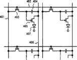
Consult Fig. 4 now, wherein show the pixel structure of an active array type luminescent device.Among the figure, source electrode line of reference number 401 expressions, the TFT (after this being referred to as switching TFT) of its on-off element effect of 402 expressions, and capacitor that is electrically connected with 403 drain electrodes of a switching TFT of 404 expressions.
The drain electrode of switching TFT 403 also is electrically connected with the grid of Current Control TFT405.The source electrode of Current Control TFT405 links to each other with power lead 406, and drain electrode and electroluminescent cell 407 wherein is electrically connected simultaneously.In other words, Current Control TFT405 can play the element that control is flowed by light-emitting component 407 electric currents.
The brightness of electroluminescent cell can be controlled by the TFT with difference in functionality is provided respectively in each pixel.As a result, light period is basically corresponding to a frame period, and can even suppress brightness simultaneously with the high precision pixel section displayed image of assigning to.In addition, the advantage of active material type comprises the shift register that can form a driving circuit that sends signal to pixel parts or at same suprabasil sample circuit.
Yet, compare with passive matrix with simple structure, be difficult to guarantee that the active array type luminescent device has enough output, because must in the same substrate of active array type device, form a plurality of TFT.Specifically, in the time driving circuit will being placed in the same substrate, can produce row effects, this moment, delegation's pixel was owing to the row defective takes place an operational deficiencies.In addition, because the manufacturing step of TFT is quite complicated, compare with the passive matrix device, the manufacturing cost possibility of active array type device can be higher.So having brought at display adopts the luminescent device electricity of active array type to send a telegraph the shortcoming of the cost increase of gas equipment.
Summary of the invention
So, the objective of the invention is in order to reduce the manufacturing cost of active matrix type displaying device, so that a cheap display device is provided.In addition, the present invention is also in order to provide a kind of not expensive electrical equipment that adopts in its display part according to display device of the present invention.
According to the present invention, in order to reduce the cost of active array display unit, the TFT of all pixel parts constitutes (can be P raceway groove or n raceway groove) with a kind of TFT of conductivity type, and driving circuit is also all used with the TFT of the same conductivity type of pixel parts and constituted.So, can significantly reduce manufacturing process, thereby reduce cost.
For above-mentioned purpose, according to an aspect of the present invention, all source electrode lines, grid, gate line (it is a lead that transmits signal to grid) and power lead all form simultaneously.In other words, on same surface, form an identical conduction film.In addition, according to another aspect of the present invention, be used for TFT is connected to and be used for interconnecting many independent gate lines that form, or source electrode line, or that line of power lead (also being referred to as connecting line in this instructions) is formed on the same surface with the same conducting film of drain electrode of Current Control TFT.
In addition, according to another important aspect of the present invention, driving circuit is that the TFT by same conductivity type constitutes.In other words, with usually that the driving circuit based on the routine of cmos circuit design of n raceway groove and the complementary combination of p channel TFT is different, driving circuit of the present invention is the TFT (TFT) that only makes up p raceway groove or n raceway groove.
Therefore, the invention provides a kind of display device, comprising: the first film transistor; Second thin film transistor (TFT) is electrically connected with a pixel electrode; Article one, gate line is electrically connected with described the first film transistor; With a source electrode line, be electrically connected with described the first film transistor, and be formed on the same surface by the conducting film identical with described gate line; A dielectric film on described gate line and described source electrode line; With the connecting line on described dielectric film; Wherein said gate line is crossed over described source electrode line by described connecting line, is formed on the same surface by the conducting film identical with described pixel electrode with wherein said connecting line.
The present invention also provides a kind of display device, comprising: the first film transistor; Second thin film transistor (TFT) is electrically connected with a pixel electrode; Article one, gate line is electrically connected with described the first film transistor; With a source electrode line, be electrically connected with described the first film transistor, and be formed on the same surface by the conducting film identical with described gate line; A dielectric film on described gate line and described source electrode line; With the connecting line on described dielectric film; Wherein said source electrode line is crossed over described gate line by described connecting line; Be formed on the identical surface by the conducting film identical with wherein said connecting line with described pixel electrode.
The present invention also provides a kind of display device, comprising: the first film transistor; Second thin film transistor (TFT) is electrically connected with a pixel electrode; Article one, gate line is electrically connected with described the first film transistor; With a source electrode line and a power lead, described source electrode line is electrically connected with described the first film transistor, is being formed on same surface by the conducting film identical with described gate line; A dielectric film on described gate line, described source electrode line and described power lead; With the connecting line on described dielectric film; Wherein said gate line is crossed over described source electrode line and described power lead by described connecting line, is formed on same surface by the conducting film identical with described pixel electrode with wherein said connecting line.
The present invention also provides a kind of display device, comprising: the first film transistor; Second thin film transistor (TFT) is electrically connected with a pixel electrode; Article one, gate line is electrically connected with described the first film transistor; With a source electrode line and a Current Control line, they are formed on the same surface by the conducting film identical with described gate line, and described source electrode line is electrically connected with described the first film transistor; A dielectric film on described gate line, described source electrode line and described Current Control line; With the connecting line on described dielectric film; Wherein said source electrode line is crossed over described gate line and described power lead by connecting line; Wherein said connecting line is formed on the identical surface by the conducting film identical with described pixel electrode.
Wherein said connecting line forms on the layer that is different from described gate line and described source electrode line.
Wherein said connecting line is made up of nesa coating.
Wherein each described the first film transistor electrically links to each other with described source electrode line, and described second thin film transistor (TFT) is the P channel thin-film transistor.
Wherein said display device is a luminescent device.
Wherein said display device is a liquid crystal display device.
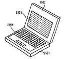
Wherein said electrical equipment is selected from by video camera, digital camera, and the goggles escope, navigational system, the voice playing device, notebook-sized personal computer, game station is in the group that portable data assistance, visual player that has disposed recording medium constitute.
The present invention also provides a kind of method that is used for making display device, comprises step: form one semiconductor layer on insulating surface; On described semiconductor layer, form a gate insulating film; On described gate insulating film, form a source electrode line, a gate line and a power lead; In described semiconductor layer, form P type second semiconductor regions of transistorized P type first semiconductor regions of the first film and second thin film transistor (TFT); On described source electrode line, described gate line and described power lead, form one deck intermediate insulating layer; Form the contact hole that arrives described source electrode line, transistorized P type first semiconductor regions of described the first film and described power lead respectively; With connecting line of formation, to be provided between transistorized P type first semiconductor regions of described source electrode line and described the first film or the electrical connection between P type second semiconductor regions of described power lead and described second thin film transistor (TFT); Wherein said source electrode line and described gate line are electrically connected to the first film transistor.
The present invention also provides a kind of method that is used for making display device, comprises step: form one semiconductor layer on insulating surface; On described semiconductor layer, form one deck gate insulator; On described gate insulator, form a gate line, a gate line and a power lead; In described semiconductor layer, form P type second semiconductor regions of the first film transistorized P-type semiconductor zone and second thin film transistor (TFT); On described source electrode line, described gate line and described power lead, form one deck intermediate insulating layer; Form and arrive P type second semiconductor regions of described source electrode line, described second film crystal and the contact hole of described power lead respectively; With the connecting line that forms a described source electrode line of leap and a plurality of gate lines of interconnection; Wherein said source electrode line and described gate line are electrically connected to the first film transistor.
Wherein said connecting line is formed on the same surface by the conducting film identical with pixel electrode, and described pixel electrode is electrically connected to described second thin film transistor (TFT).
Wherein said display device is a luminescent device.
Wherein said display device is a liquid crystal display device.
Wherein said display is incorporated into from by video camera, the number camera, the goggles escope, navigational system, the voice playing device, notebook-sized personal computer, game station, in the electrical equipment of electing in a group that portable data assistance, visual player that has disposed recording medium constitute.
The present invention also provides a kind of display device, comprising: the first film transistor; Second thin film transistor (TFT) is electrically connected with a pixel electrode; Article one, gate line is electrically connected with described the first film transistor; With a source electrode line, be electrically connected with described the first film transistor, and be formed on the same surface by the conducting film identical with described gate line; Be formed on the interlayer dielectric on above-mentioned gate line and the described source electrode line; With the connecting line that is formed on the described interlayer dielectric; Wherein said gate line extends across described source electrode line by connecting line; Wherein said connecting line is formed on the same surface by the conducting film identical with described pixel electrode.
Wherein said connecting line is made up of nesa coating.
Wherein the described source electrode line of each described the first film transistor AND gate is electrically connected, and described second thin film transistor (TFT) is the P channel thin-film transistor.
Wherein said display device is a luminescent device.
Wherein said display device is a liquid crystal display device.
Wherein said electrical equipment is selected from by video camera, digital camera, and the goggles escope, navigational system, the voice playing device, notebook-sized personal computer, game station is in the group that portable data assistance, visual player that has disposed recording medium constitute.
The present invention also provides a kind of display device, comprising: the first film transistor; Second thin film transistor (TFT) is electrically connected with a pixel electrode; Article one, gate line is electrically connected with a pixel electrode; With a source electrode line, be electrically connected with a pixel electrode, and be formed on the same surface by the conducting film identical with described gate line; Be formed on the interlayer dielectric on above-mentioned gate line and the described source electrode line; With the connecting line that is formed on the described interlayer dielectric; Wherein said source electrode line extends across described gate line by connecting line; Be formed on the identical surface by the conducting film identical with wherein said connecting line with described pixel electrode.
Wherein said connecting line is made up of nesa coating.
Wherein each described first electrically links to each other with described source electrode line, and described second thin film transistor (TFT) is the P channel thin-film transistor.
Wherein said display device is a luminescent device.
Wherein said display device is a liquid crystal display device.
Wherein said electrical equipment is selected from by video camera, digital camera, and the goggles escope, navigational system, the voice playing device, notebook-sized personal computer, game station is in the group that portable data assistance, visual player that has disposed recording medium constitute.
Description of drawings
Fig. 1 shows the structure of gate side drive circuit;
Fig. 2 shows the timing diagram of decoder input signal;
Fig. 3 shows the structure of source side drive circuit;
Fig. 4 shows the circuit structure of the pixel parts of luminescent device;
Fig. 5 shows the cross-section structure of the pixel parts of luminescent device;
Fig. 6 shows the top view structure of the pixel parts of luminescent device;
Fig. 7 (A) and 7 (B) show another cross-section structure of the pixel parts of luminescent device separately;
Fig. 8 (A)-8 (D) shows the various manufacturing steps of luminescent device;
Fig. 9 (A)-9 (C) shows the various manufacturing steps of luminescent device;
Figure 10 shows another circuit structure of the pixel parts of luminescent device;
Figure 11 shows another circuit structure of the pixel parts of luminescent device;
Figure 12 (A)-12 (C) shows the various manufacturing steps of luminescent device;
Figure 13 shows top view structure of Chinese alligator of the pixel parts of luminescent device;
Figure 14 (A)-14 (C) shows the various manufacturing steps of luminescent device;
Figure 15 (A) shows another top view structure of the pixel parts of luminescent device;
Figure 15 (B) shows another cross-section structure of the pixel parts of luminescent device;
Figure 16 (A) and 16 (B) show another circuit of the pixel parts of luminescent device;
Figure 17 (A) and 17 (B) show another circuit structure of the pixel parts of luminescent device;
Figure 18 shows the film former that forms electroluminescence layer;
Figure 19 (A) and 19 (B) show the profile of liquid crystal display device;
Figure 20 (A)-20 (F) shows the object lesson of electrical equipment respectively; With
Figure 21 (A)-21 (D) shows the object lesson of electrical equipment respectively.
Embodiment
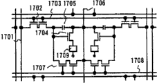
Now consult Fig. 1 and Fig. 2, description is used for driving circuit of the present invention.According to the present invention, substituted common shift register with the demoder of the employing P channel TFT of Fig. 1.Fig. 1 shows an example of gate side drive circuit.
Among Fig. 1, numeral 100 is represented the demoder of gate side drive circuit, and 101 represent the buffer part of gate side drive circuit.Here, buffer partly has been meant the part of a plurality of buffers (buffer amplifiers) integrated.In addition, buffer is meant that one can be forbidden driving and subsequent step can not produce dysgenic circuit to former step.
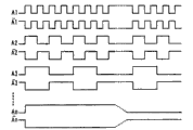
Gate electrode side demoder 100 is described now.The input signal cable (below be referred to as selection wire) of numeral 102 expression demoders 100 is used A1 particularly, A1 (have the signal A2 anti-phase with A1, A2 (having the signal anti-phase) with A2 ..., An and An (have the signal anti-phase with An.In other words, can think that one has 2n bar selection wire.
The number of selection wire is according to determining from the number of gate line that grid are surveyed the output of driving circuit.For example, under the situation of the pixel parts that has disposed the VGA display, require to have 480 gate lines, this requires to have altogether 18 selection wires conversely and offers 9 bits (corresponding to n=9).Selection wire 102 sends the timing signal of Fig. 4.As shown in Figure 2, suppose that the frequency of A1 normally is 1, then the frequency of A2 can be expressed as 2
-1, the frequency of A3 can be expressed as 2
-2, the frequency of An can be expressed as 2
-(n-1)
Numeral 103a represents first order NAND circuit (being also referred to as the NAND unit), and 103b and 103c represent the second level and n level NAND circuit.The number of required NAND circuit equals the number of gate line, specifically, requires n NAND circuit here.In other words, demoder 100 of the present invention is made up of a plurality of NAND circuit.
In each NAND circuit 103a-103c, P channel TFT 104 to 109 is combined into NAND circuit altogether.In fact, each NAND circuit 103 uses 2n TFT.In addition, the grid of each P channel TFT 104 to 109 and selection wire 102 (A1, A1 ..., An, An) wherein one link to each other.
In this case, in NAND circuit 103a, P channel TFT 104 to 106 has respectively and A1, A2 ..., the continuous grid of An (being called positive selection wire), and parallel with one another, be also connected to positive supply lead (V as public source
DH) 110 and as the output line 111 of public drain electrode.On the other hand, remaining P channel TFT 107 to 109 has respectively and A1, A2 ... An, (being called negative selection wire) continuous grid, and mutually series connection are positioned at source electrode negative power line (V then of the TFT109 of circuit one end
DL) 112 link to each other, the drain electrode that is positioned at the TFT107 of the circuit other end then links to each other with output line 111.
As mentioned above, NAND circuit of the present invention comprises n TFT of the parallel connection of n the TFT of series connection of same conductivity type (this example is the P channel TFT) and other same conductivity type (this example is the P channel TFT).Should be realized that in n NAND circuit 103a-103c, the combination between all P channel TFT and the selection wire is mutually different.In other words, output line 111 to dispose make in them have only one selected, and when the selection wire input signal, output line 111 is sequentially selected from the one side.
So buffer 101 is made up of to 113c a plurality of buffer 113a, so that enable respectively corresponding to NAND circuit 103a-103c.Should be realized that buffer 113a-113c can have same structure.
In addition, impact damper 113a-113c is made up of the P channel TFT 114-116 of same conductivity type.Be input to the grid of corresponding P channel TFT (the first same conductivity type TFT) from the output line 111 of demoder.P channel TFT 114 utilizes ground power lead (GND) 117 as its source electrode, and gate line 118 is as its drain electrode.In addition, P channel TFT 115 (the second same conductivity type TFT) land used power lead 117 is as its grid, positive power line (V
DH) 119 be its drain electrode as its source electrode and gate line 118.P channel TFT 115 always is in ON (leading to) state.
In other words, each buffer 113a-113c of the present invention comprises first with conductivity type TFT (P channel TFT 114), also comprise link to each other with an above-mentioned TFT second with conductivity type TFT (P channel TFT 115), with the grid of a TFT as drain electrode.
In addition, P channel TFT 116 (the 3rd with conductivity type TFT) adopts a reseting signal line (Reset) as its grid, and positive power line is drain electrode as its source electrode and gate line 118.Should be realized that ground power lead 117 can replace with negative power line (be a power lead, be used to provide voltage and make the P channel TFT be used as the on-off element of the pixel that is in the ON state).
In this case, the channel width (W2) of channel width of a P channel TFT 115 (W1) and P channel TFT 114 satisfies the relation of W1<W2.Channel width is meant the length of the channel formation region of measuring on perpendicular to orientation.
Buffer is following to carry out work.During positive voltage was added to output line 111, P channel TFT 114 was in OFF (closing) state (promptly not forming raceway groove).On the other hand, because P channel TFT 115 always is in ON state (promptly forming raceway groove), so the voltage of positive power line 119 is added on the gate line 118.
On the other hand, when negative voltage was added to output line 111, P channel TFT 114 entered out state.At this moment, because the channel width of P channel TFT 114 is wideer than the width of P channel TFT 115, the current potential of gate line 118 is driven by the output of P channel TFT 114 1 sides, makes the current potential of ground power lead 117 be added to gate line 118.
So, gate line 118 output negative voltages when negative voltage is added to output line 111 (the P channel TFT is used as be in the ON state pixel switch element) just (make the P channel TFT be used as the on-off element of the pixel that is in the OFF state) and always export a positive electricity when positive voltage is added to output line 111.
P channel TFT 116 is used as and makes gate line 118 be coupled with the reset switch of positive voltage, and it always is added with negative voltage.In other words, after the selection cycle of gate line 118 is finished, promptly import a reset signal, like this positive voltage is added on the gate line 118.Should be realized that P channel TFT 116 can be omitted.
Gate side drive circuit with being operated in aforesaid way comes the select progressively gate line.Fig. 3 then shows the structure of source side drive circuit.Source side drive circuit shown in Figure 3 comprises a demoder 301, latch 302 and buffer 303.Because demoder 301 has the structure identical with the gate side drive circuit with buffer 303, so omission is to its description.
Under the situation of the source side drive circuit of Fig. 3, latch 302 is made up of first order latch 304 and second level latch 305.The described first order latchs 304 and comprises a plurality of elementary cell 307a, and each elementary cell 307a is made up of m P channel TFT 306a-306c.Output line from demoder 301 links to each other with m TFT 306a-306c of work, has so just formed elementary cell 307.Should be realized that number m is any integer.
For example, when the situation of VGA display, the number of source electrode line is 640.Under the situation of m=1, the number of the NAND circuit that need provide also is 640, requires to provide 20 selection wires (corresponding to 10 bits) simultaneously.Yet on the other hand, when m=8, the NAND circuit number that must want is 80, and necessary selection wire number is 14 (corresponding to 7 bits).In other words, suppose that the source electrode line number is M, then essential NAND circuit number is M/m.
The source electrode of P channel TFT 306a-306c be connected respectively to vision signal (V1, V2 ..., VK) 309.In other words, when negative voltage was added to output line 308, all P channel TFT 306a-306c were entered the ON state simultaneously, thereby vision signal is sent to corresponding TFT306a-306c respectively.So vision signal is remained on respectively among the coupled capacitor 310a-310c.
In addition, second level latch 305 also comprises a plurality of each elementary cell 307b that are made up of P channel TFT 311a-311c.The grid of all P channel TFT 311a-311c links to each other with latch signal line 312, and when negative voltage was added to latch signal line 312, all P channel TFT 311a-311c were by the while conducting like this.
Like this, the signal that remains among the capacitor 311a-311c is remained on the 313a-313c that links to each other with TFT311a-311c respectively, and outputs to buffer 303 simultaneously.Then, as described to Fig. 1, these signals are output to source electrode line 314 by buffer.Source side drive circuit in order to the work of foregoing description mode is connected in turn source electrode line.
As mentioned above, combined by being P channel TFT gate side drive circuit and source side drive circuit, all pixel parts and driving circuit can be made up of the P channel TFT fully.So yield rate and technology are improved greatly, manufacturing cost is reduced.
Should be realized that, even can be configured on the outside integrated circuit (IC) chip that connects source side drive circuit or gate side drive circuit or both and implement the present invention.
Embodiment 1
Except driving circuit, pixel parts is made up of the P channel TFT fully in the present invention.Existing description comes the structure of the pixel parts of displayed image in an embodiment of the present invention according to the signal that is sent by as shown in figs. 1 and 3 driving circuit.
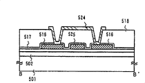
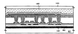
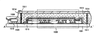
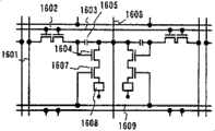
The structure of the pixel of active matrix light emitting device of the present invention has been shown in Fig. 5 and 6.Fig. 5 shows the cut-open view of pixel one by one, and Fig. 6 exports the top view of adjacent two pixels.Fig. 5 shows along the cut-open view of the A-A ' hatching line of Fig. 6, and same ingredient is represented with prosign in two figure.In addition, two pixels that show in Fig. 6 and power lead are symmetries mutually, and therefore, signal has identical structure.
Among Fig. 5, the substrate of numeral 501 expression printing opacities, and 502 expressions comprise the insulation course of silicon.Can use substrate of glass, quartz substrate, the crystal glass substrate, or plastic-substrates all can be used as (comprising plastic sheeting) substrate 501 of printing opacity.Silicon oxide layer, or silicon nitride all can be used as the dielectric film 502 that comprises silicon.
In this manual, TFT is formed on the insulation course.Dielectric film (dielectric film that normally comprises silicon) or the substrate (normally quartz substrate) of being made by insulator all can be used as insulation course.So wording " on insulation course " means at " on dielectric film " or " on by substrate made of insulating material ".
On the dielectric film 502 that comprises silicon, form switching TFT 601 and Current Control TFT602 with some P channel TFT.Switching TFT 601 adopts to comprise the regional 503-505 (after this being referred to as the P-type semiconductor district) that is made by P-type semiconductor and comprise by intrinsic-OR to be that the zone 406 of intrinsic semiconductor (after this being referred to as channel formation region) and 507 semiconductor regions are as active layer basically.On the other hand, Current Control TFT602 with comprise P- type semiconductor zone 508 and 509 and the semiconductor region in channel formation region territory 510 as active layer.
P- type semiconductor district 503 or 505 is used as the source area or the drain region of switching TFT 601.In addition, P-type semiconductor district 508 is used as the source area of Current Control TFT602, and P-type semiconductor 509 is used as the drain region of Current Control TFT602.
The active layer of switching TFT 601 and Current Control TFT602 covers with gate insulating film 511, and forms source electrode line 512 thereon, grid 513a, grid 513b, drain line 514 and grid 515.These elements form simultaneously with same material.Can use tantalum, tungsten, molybdenum, the nitride of niobium titanium or these materials is as the constituent material of these lines or electrode.In addition, can use by the alloy of these combinations of materials or the silicide of these materials.
In addition, as shown in Figure 6, drain line 514 combines with grid 515.In addition, grid 513a and 513b combine with common gate polar curve 516, and same like this voltage always is added to these grids 513a and 513b.
In addition, in Fig. 5, passivating film of making by the silicon oxides of nitrogen of numeral 517 expressions, or silicon nitride, an interlayer insulating film 518 forms thereon.A dielectric film that comprises silicon or organic resin can be used as interlayer insulating film 518.Kapton, acrylic resin film or BCB (benzocyclobutene) film can be used as organic resin film.
In addition, on interlayer insulating film 518, connecting line 519-522 and electrode 523 that nesa coating is made have been formed.Simultaneously, line 524 as shown in Figure 6 also forms simultaneously.Indium oxide, tin-oxide, zinc oxide, the compound of indium oxide and tin-oxide, the compound of tin-oxide and zinc oxide, or sow the compound that these materials obtain and all can be used as nesa coating by additional.
In this case, connecting line 520 is the lines that electrical connection is provided between source electrode line 512 and P-type semiconductor district 503, and connecting line 521 is the lines that electrical connection is provided between P-type semiconductor trivial 505 and drain line 514.In addition, connecting line 522 is the lines that electrical connection is provided between source area 508 and power lead 525 (see figure 6)s.
Fig. 7 (A) shows a cut-open view of cutting acquisition along the B-B ' line of Fig. 6 open.Shown in Fig. 7 (A), connecting line is crossed over line of electric force 525, and is provided at the connection between the gate line 516.In addition, Fig. 7 (B) shows the cut-open view that obtains by along Fig. 6 C-C '.Shown in Fig. 7 (B), connecting line 522 is electrically connected the P-type semiconductor district 508 of Current Control TFT602 with power lead 525.
In this actual device, on pixel capacitors 523 (not shown), form an electroluminescence layer and negative electrode (not shown) to finish the luminescent device of an active array type.Electroluminescence layer and negative electrode can form with knowing technology.
In addition, though, described as an example above and had top gate structure that () TFT specifically, a planar shaped TFT, the present invention and the limit are in this class TFT.In addition, the present invention can be applicable to have the TFT of bottom grating structure.In general, available anti-phase-joining type TFT to implement the present invention.
Adopt aforesaid pixel structure, the manufacturing process of active array type luminescent device can obtain simplifying, thereby can make the cheap active array type luminescent device of bid.In addition, can realize adopting the electronic equipment the same with the display part.
Embodiment 2
In the present embodiment, the manufacturing process of active array type luminescent device is described in 8 (A)-8 (D) and 9 (A)-9 (C) in conjunction with the accompanying drawings now, and wherein pixel parts and being used for driving circuit from signal to pixel parts that send is formed on the same dielectric layer.
At first, shown in Fig. 8 (A), counterdie (insulator) 802 is formed on the substrate of glass 801.In the present embodiment, counterdie 802 be by from the side that approaches substrate of glass 801 sequentially deposition thickness be the second silicon oxynitride film of thickness of 50 nanometers and the silicon oxides of nitrogen that thickness is 200 nanometers.The nitrogen content of the first silicon oxynitride film is bigger than the content of the second silicon oxynitride film, so that compacting silicon metal is from the diffusion of substrate of glass.
Then, on counterdie, form the noncrystalline silicon film (not shown) that a layer thickness is 40 nanometers with the plasma CVD method.After this, the indefiniteness silicon fiml with the laser emission crystallization to form a polysilicon film (many silicon fimls) 803.Should be realized that available microcrystalline sillicon film or noncrystal SiGe film replace noncrystalline silicon film.In addition, a kind of crystallization method is not limited to the laser crystallization method, but any other crystallization method all can be used.
Then, shown in Fig. 8 (B), polysilicon film 803 is formed be patterned into independently insulator-semiconductor layer 804-806 respectively.After finishing, become an active layer of forming the TFT of a driving circuit (this TFT is referred to as driver TFT) with numeral 804 semiconductor layers of representing.On the other hand, become the former layer of having of switching TFT with numeral 805 semiconductor layers of representing, and numeral 806 expressions is the active layer of Current Control TFT.
After this, the thickness of being made up of silicon oxide film is that the gate insulating film 807 of 80 nanometers is with plasma CDV method shape, so that cover the semiconductor layer 804-806 of insulation.In addition, the tungsten film (not shown) forms by sputter on gate insulating film 807, and its thickness is 350 nanometers, is patterned to gate electrode 808,809 then, 810a, 810b.Simultaneously, form the source electrode line 812 and the drain line 813 of switching TFT.Certainly, drain line 814 and grid 811 form.
Then, the element of the periodic table of elements 3 families is impregnated in grid 808,809,810a, and 810b, and source electrode line 812 and drain line 813 are used as mask.Any method can be used above-mentioned purpose.In the present embodiment, use the plasma doping method with 5 * 20
29-1 * 10
21Atomicity/cm
3Concentration adds boron.So, semiconductor region (the being referred to as the P-type semiconductor district later on) 814-821 of formation P-type conduction.In addition, channel formation region 822-826 is formed directly into grid 808,809, below 810a and the 810b.
Should be realized that in the present embodiment, P- type semiconductor district 814 and 816 is used as the source area of the P channel TFT that forms driving circuit, and P-type semiconductor district 815 is used as the drain region of the P channel TFT that forms driving circuit.
After this, heat-treat element in 3 families that activate the periodic table of elements that is included in the P-type semiconductor district.This activate to handle available smelting furnace annealing method, or the laser annealing method, the light annealing method, or any their combined method is finished.In the present embodiment, thermal treatment is to carry out under 500 ℃ 4 hours in blanket of nitrogen.At this moment, preferably reduce the concentration of the oxygen in the blanket of nitrogen to alap degree.The active layer of TFT is handled by above-mentioned activation and is formed.
After activation was finished dealing with, the silicon oxynitride film that forms a layer thickness 200 nanometers was carried out the hydrogen treatment of semiconductor layer then as passivating film.Any hydrogen annealing technology or plasma hydrogenization technology all can be used for hydrogen treatment.Can obtain the structure shown in Fig. 8 (C) like this.
Then, shown in Fig. 8 (D), formation thickness is the intermediate insulating film 828 that the resin of 800 nanometers is made.Available polyimide, polyamide, acryl resin, epoxy resin or BCB (benzocyclobutene) are as resin.In addition, also can use inorganic insulating membrane.
In intermediate insulating film 828, form the contact hole then, and form connecting line 829-835 and pixel capacitors 836.In the present embodiment, by the compound (indium tin oxide of indium oxide and tin-oxide; ITO) conducting film of making is used to form connecting line 829-835 and pixel capacitors 836.Should be realized that the conducting film of any printing opacity of being made by other materials all can use.
In the state of foregoing description, finished the P channel TFT that forms driving circuit and in Current Control TFT and the switching TFT of pixel parts.In the present embodiment, all TFT are P channel-types.Should be noted that switching TFT forms like this: make grid cross over active layer, be one another in series so that two different channels form the district two different positions.Such structure can be suppressed OFF (shutoff) current value (that is the electric current that, suppresses TFT OFF state) effectively.
Then, as Fig. 9 (A), form marginal portion and concave part (owing to contacting the recess that the hole forms) that the insulator 837 and 838 that is formed from a resin covers pixel capacitors 836.These insulators 837 and 838 can be by forming insulation film that one deck is formed from a resin and it graphically being formed.In this case, need will be from the surface of pixel capacitors 836 to the height setting at the top of cutting off body 838 in 300 nanometers or evening little (being preferably 200 nanometers or littler).Should be noted that insulator 837 and 838 can omit.
Thereby forming insulation course 837 is deleterious effects of avoiding the electric field density of marginal portion for the marginal portion that covers pixel capacitors 836.So, can prevent degenerating of electroluminescence layer.On the other hand, the purpose of formation insulator 838 is in order to bury because the concave part of the pixel capacitors that the contact hole forms.Any covering defective of the electroluminescence layer of Xing Chenging can be avoided so after a while, and the short circuit between pixel parts and negative electrode.
Then, thickness is that the electroluminescence layer 839 of 70 nanometers and negative electrode 840 usefulness vapour deposition methods that thickness is 300 nanometers form.In the structure of present embodiment, thickness is that the copper double-fermented wine cyanine layer (hole injection layer) and the thickness of 20 nanometers is the Alq of 50 nanometers
3(luminescent layer) forms electricity to luminescent layer 839.Should be realized that, hole injection layer, hole transmission layer, combined any known other structures of electron transfer layer or electron injecting layer all can be used for luminescent layer.
In the present embodiment, at first form copper phthalocyanine layer and cover all pixel capacitors, for red, green and blue look forms the red luminescent layer of one deck respectively, green luminescent layer and blue luminescent layer.The zone that forms this layer can utilize shadow mask to select according to evaporation.So just, can realize colored the demonstration.
In the time will forming green luminescent layer, Alq
3(the 3-8-quinolinol closes compound) is used as the parent material of luminescent layer, and quinacridone or coumarin 6 are used as alloy.When forming red light luminescent layer, Alq is used as the parent material of luminescent layer, and DCJT, DCM, or DCM2 is used as alloy.When forming the blue streak luminescent layer, BALq (having 2-methyl-8-quinolinol and amphyl) is used as the parent material , Er of luminescent layer, and perylene is used as alloy.
Should be realized that the present invention is not limited to use above-mentioned organic material, but the organic light emission electroluminescent material of available any known low molecule-type, the polymer electrolyte electroluminescent organic material, or inorganic electroluminescence material all can use.In addition, the combination of any of these material all can be used.In addition, under the situation of using the polymer electrolyte organic material, can use the coated method.
As mentioned above, electroluminescent cell is by pixel capacitors (anode) 836, electroluminescence cause 839 and negative electrode 840 form (seeing Fig. 9 (B)).
Then, the lattice cover piece is bonding with bonding agent 841.In the present embodiment, substrate of glass is used as covering 842.In addition, a flexible plastic films, a quartz substrate, a plastic-substrates, a metallic substrates, a silicon base, or ceramic bases can be used.Advantageously, the dielectric film that will comprise silicon or carbon membrane places and is exposed on the airborne surface, in case block gas or water enter or provide scuffing to being caused by friction.
The UV castable resin, or heat reactive resin is often used as and is bonding agent 841.For example, PVC, acrylic acid, the inferior acid of polyamides, epoxy resin, the silicic acid resin, PVB, or EVA can use.It seems that from electroluminescent cell bonding agent 841 is to be positioned at the position of approaching the observer, at this moment, it is to be made by the material that can allow light pass through that bonding agent requires.In addition, advantageously, in bonding agent 841, provide a kind of absorbent material (preferably ba oxide), and/or oxidation-resistant material (that is oxygen-absorbing material) prevents the degeneration of electroluminescent cell.
Adopt said structure, electroluminescent cell can bar out air fully.So,, thereby improved the reliability of synthetic electroluminescent cell greatly because oxidation makes the degeneration of electroluminescent material obtain compacting basically.
The active array type luminescent device of Zhi Zaoing has the circuit structure that comprises as shown in figure 10 in the above described manner.Specifically, in Figure 10, source electrode line of numeral 1001 expressions, switching TFT of gate line of 1002 expressions 1003 expressions, Current Control TFT of 1004 expressions, power lead of 1005 expressions and light-emitting component of 1006 expressions.In the present embodiment, each switching TFT 1003 and Current Control TFT1004 form the P channel TFT.
Should be noted that the grid capacitance of Current Control TFT1004 presents the same effect of adopting with routine techniques of capacitor (being the capacitor 404 of Fig. 4).This is understandable, because, realizing the time-division with digital drive scheme during gray level display, have only grid capacitance could keep essential electric charge, because the cycle of a frame (or a field duration) is too short with Current Control TFT.
Aforesaid active array type luminescent device of the present invention only needs 5 masks to carry out graphical step (when insulator 837 and 838 omitted, this number also can reduce) altogether, and this just can realize the high yield low-cost production.
Embodiment 3
In the above-described embodiments, the circuit structure of the described pixel parts of Figure 10 can be changed into shown in Figure 11.Specifically, in Figure 11, numeral 1101 expression source electrode lines, 1102 expression gate lines, 1103 expression switching TFT, 1104 expression Current Control TFT, 1105 expression power leads and 1106 expression electroluminescent cells.In the present embodiment, each switching TFT 1103 and Current Control TFT1104 form the P channel TFT.
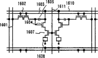
In this case, because gate line 1102 and power lead 1105 place different layers, help disposing these elements so that overlap each other and intermediate insulating layer is inserted between them.So it is public that the occupied zone of these lines can be made basically, thereby can increase effective launch site of pixel.
Embodiment 4
In the present embodiment, the active array type luminescent device is to use the mode different with embodiment 1 to make.Now consult Figure 12 (A)-12 (C) and describe manufacturing process.
At first, until the manufacturing step such as the front in that step shown in Fig. 8 (D) form connecting line 1201-1207 and drain line 1208 as described in embodiment 2.In the present embodiment, these connecting lines are made up of metal pattern.Though any material can be used as metal pattern, adopted layered membrane in the present invention with 3-tier architecture, the layer of aluminum film is clipped between the titanium film.
Then, shown in Figure 12 (B), form the pixel capacitors of making by nesa coating 1209.In this case, make pixel capacitors 1209 form to such an extent that allow this part enter to contact with drain line 1208.So Current Control TFT and pixel capacitors can be electrically connected mutually.Figure 13 shows the top view of said structure.The sectional view of Figure 12 (B) is the sectional view along the A-A ' line of Figure 13.
In the present embodiment, connecting line 1201-1207 available metal film is made.Like this, compare, can reduce conductor resistance and contact resistance with the similar film of describing such as the embodiment of ITO film or front.And all are used in driving circuit connecting the line of various circuit parts and all can be made by the low resistance metal film, therefore, can realize presenting the driving circuit of high operation speed.
Though pixel capacitors 12-9 forms after connecting line 1201-1207 and drain line 1208 are finished, this makes order and can put upside down.In other words, can after the pixel capacitors formation that nesa coating is made, form connecting line and the drain line of making by metal film.
Then,, form the insulation course 1210 that is formed from a resin, form electroluminescence layer 1211 and negative electrode 1212 more successively as embodiment 2.And then, form cover piece 1214 with bonding agent 1213.Like this, just finished the active array type luminescent device shown in Figure 12 (C).
Embodiment 5
In the present embodiment, an example making the active array type luminescent device of the present invention that adopts plastic-substrates or plastic foil be described.The plastics that can be used for present embodiment comprise PES (tygon sulfile) PC (polycarbonate) or PEN (tygon terephthalate).
At first, on substrate of glass 801, form TFT and electroluminescent cell as the manufacturing step of describing among the embodiment 2.In the present embodiment, yet, one deck peeling layer 1401 between substrate of glass 801 and counterdie 802, formed, shown in Figure 14 (A).Semiconductor film can be used as peeling layer 1401.Usually, noncrystalline silicon film can be used for above-mentioned purpose.
In addition, in the present embodiment, cover piece 1403 is bonding with first bonding agent 1402.Be used as first bonding agent 1402 by power fat (normally polyimide, acryl resin, amino-compound or epoxy resin).Should be realized that, when with halogen-containing fluoride etching peel ply, require the material of first bonding agent 1402 can realize sufficient selection rate.The PET film can be used as the cover piece bonding with first bonding agent 1402 in the present embodiment.
Then, the whole substrate that forms element is exposed in the gas of halogen-containing fluoride, this processing makes peeling layer 1401 quilt by selectively removing.Haloid fluoride is meant the material (X represents the halogen except fluoride, and n is an integer) that a kind of available chemical formula XFn represents.Haloid fluoride for example, chlorine monofluoride (CIF) chlorine trifluoride (CIF
3), bromine monofluoride (BrF), bromine trifluoride (BrF
3), iodine monofluoride (IF), iodine trifluoride (IF
3) can be used as haloid fluoride.
Haloid fluoride is presented on a big selection rate between silicon fiml and the silicon oxide layer, therefore can realize the selective etch of silicon fiml.In addition, this etching reaction can at room temperature be handled easily, therefore, can even can also carry out this processing after low thermal resistance capacity electroluminescent cell forms.
Though only silicon fiml is exposed in the above-mentioned haloid fluoride and can realizes etching, other fluorides (carbon tetrafluoride (CF
4) or the nitrogen tetrafluoride) also can be used for the present invention, as long as they are placed under the plasmoid.
In the present embodiment, CIF
3Be used as the nitrogen fluoride, nitrogen is used as diluents.Argon, helium, neon can be used as diluents.The flow velocity of two kinds of gases can be set in 500sccm (8.35 * 10
- 6m
3/ s) and reaction pressure can be set at 1 to 10 torr (1.3 * 10
2-1.3 * 10
3Crust) in the scope.In addition, heat treatment temperature can be set in room temperature (usually at 20-27 ℃).
Then, shown in Figure 14 (C), with the 1404 bonding substrates of making (bonding substrate) 1405 of second bonding agent by plastic-substrates or plastic resin.In the present embodiment, the PET film is used as bonding substrate 1405.Require cover piece 1403 and bonding substrate 1405 by same made to satisfy the stress equilibrium state.
So just can obtain to accompany between TFT and electroluminescent cell the active array type luminescent device of plastic foil.Because plastic foil is bonding after TFT forms in the present embodiment, so to manufacture process without limits.For example, TFT can not consider that the thermal resistance capacity of the plastics that will adopt forms TFT.
In addition, the light luminescent device because can obtain flexible, the device in the present embodiment is suitable for such as mobile phone, the display part of the portable information device of electronic databank etc.
The described structure of present embodiment can be freely with embodiment 1-4 in any structure combined.
Embodiment 6
In the present embodiment, be preferably in an one or both sides configuration DLC (class diamond carbon) film of the substrate that will form on TFT and the electroluminescent cell or cover piece.The thickness that is noted that this DLC film is not more than 50nm (being preferably in the 10-20 nanometer) asking, because too big thickness can reduce the transparency of film.In addition, the DLC film can form with sputter or ECR plasma CVD method.
The feature of DLC film is that the distribution of Raman spectrum comprises one at 1550cm
-1A dissymmetric peak.In addition, the feature of DLC film is that its hardness is clung at 15-25 when utilizing little Thickness measuring instrument to measure.In addition, best, configuration DLC film has bigger hardness and thermal capacity as the diaphragm of stress protection surface and/or heat radiation because compare the DLC film with the substrate of cover piece.
The structure of describing as present embodiment can be freely with embodiment 1-5 in any structure combined.
Embodiment 7
The profile of the luminescent device of the present invention of embodiment 2 will be described in the present embodiment.Figure 15 (A) shows the top view of luminescent device of the present invention, and Figure 15 (B) shows its sectional view.
At Figure 15 (A), substrate of numeral 1501 expressions, pixel parts of 1502 expressions, source side drive circuit of 1503 expressions and 1504 expression gate side drive circuit.Each these driving circuit links to each other with a FPC (flexible printed circuit) 1506 by lead 1504, and then links to each other with external unit.The gate electrode side circuit that is shown in Fig. 1 is used to the gate side drive circuit 1504 of Figure 15 (A), and the source side drive circuit that is shown in Fig. 3 is used for the pixel parts 1502 of Figure 15 (A).In addition, pixel parts shown in Figure 5 is used to the pixel parts 1502 of Figure 15 (A).At this moment, form 1512, one bonding agents 1513 of 1511, one cover pieces of one first seal (seeing Figure 15 (B)), so that around pixel parts 1502, source side circuit 1503 and gate side drive circuit 1504.
Figure 15 (B) is corresponding to the cut-open view along Figure 15 (A) A-A '.In this case, therefore 1500 area surrounded of dotted line no longer describe in detail corresponding to the sectional view of Fig. 9 (C).
The negative electrode of electroluminescent cell is electrically connected with the regional interior line of representing with numeral 1,515 1505.Lead 1505 is used for providing a predetermined voltage to negative electrode, and links to each other with FPC1506 by anisotropic conductive film 1516.In addition, electroluminescent cell is surrounded by first seal 1511 and cover piece 1512, and cover piece then is adhered to substrate 1501 with first seal 1511.Electroluminescent cell is sealed by bonding agent 1513 glue.
In addition, bonding agent 1513 comprises a packing ring.Form if packing ring is a barium, then packing ring can have water-intake capacity.Be furnished with under the situation of packing ring, be preferably on the negative electrode resin molding of configuration as cushion to alleviate the pressure of packing ring.
At this, in the present embodiment, be furnished with the part that second seal 1514 covers the expose portion and the FPC of first seal 1511, electroluminescent cell can separate fully with air like this.Obtain to have the luminescent device of the cross section structure shown in Figure 15 (B) thus.Luminescent device in the present embodiment can be freely with embodiment 1-6 in any structure combined.
Embodiment 8
In the present embodiment, will consult the pixel structure that Figure 16 (A) and 16 (B) describe luminescent device of the present invention.In the present embodiment, the source electrode line of numeral 1601 expression switching TFT 1602, the gate line of 1603 expression switching TFT 1602,1604 expression Current Control TFT, 1605 expression capacitors (can omit), 1606 expression power leads, 1607 expression power control lines.In this case, above-mentioned source electrode line 1601, gate line 1603 power leads 1606 are to form on the identical conducting film in one deck with power control line 1609.
Work about power supply control TFT1607 can be consulted Japanese patent application No.11-341272.Be noted that in the present embodiment power supply control TFT is the P channel-type, and is the same with the structure of Current Control TFT.
Though in the present embodiment, disposed power supply control TFT1607 between Current Control TFT1604 and electroluminescent cell 1608, configuration Current Control TFT1604 also is fine between power supply control TFT1607 and electroluminescent cell 1608.In addition, power supply control TFT1607 is preferably formed as to such an extent that have the structure the same with Current Control TFT1604, or is in series with Current Control TFT1604, utilizes identical active layer simultaneously.
Figure 16 (A) shows one and shares an example of power lead 1606 with two pixels.More particularly, form two pixels mutually symmetrically with respect to power lead 1606.In this case, can reduce essential power lead number, so just can form pixel parts with higher precision.On the other hand, Figure 16 (B) shows that a power lead 1610 is arranged in parallel with gate line 1603 and a example that Current Control line 1611 and source electrode line 1601 are arranged in parallel.
The structure of describing at present embodiment can be freely combines with any structure among the embodiment 1-7.
Embodiment 9
In the present embodiment, will consult the pixel structure that Figure 17 (A) and 17 (B) describe luminescent device of the present invention.In the present embodiment, the source electrode line of numeral 1701 expression switching TFT 1702, the gate line of 1703 expression switching TFT 1702,1704 expression Current Control TFT, 1705 expression capacitors (can omit), 1706 expression power leads, 1707 expression demagnetization TFT, demagnetization gate line of 1708 expressions and electroluminescent cell of 1709 expressions.In this case, source electrode line 1701, gate line 1703, power lead 1706 is formed on one deck by identical conducting film with demagnetization gate line 1708.Can consult the principle of work of the relevant torrential magnetic TFT1707 of Japanese patent application NO.11-338786 understanding.Be noted that in the present embodiment power supply control TFT forms the P channel-type, it has the structure identical with Current Control TFT.In above-mentioned Japanese patent application.The demagnetization gate line is referred to as demagnetization signal line.
The drain electrode of demagnetization TFT links to each other with the grid of Current Control TFT, like this, and the grid voltage forcibly changing of Current Control TFT1704.Preferably demagnetization TFT is formed the P channel TFT, have the structure the same, can reduce cut-off current like this with switching TFT.
Figure 17 (A) shows the example that relevant two pixels are shared power lead 1706.That is, two pixels are symmetrically formed mutually with respect to power lead 1706.In this case, can reduce the number of essential power lead.On the other hand, to show power lead 1710 be parallel with gate line 1703 to Figure 17 (B) and demagnetization gate line 1711 is examples parallel with source electrode line 1701.
The structure that present embodiment is described can freely combine with any structure of embodiment 1-7.
Embodiment 10
Luminescent device of the present invention can adopt the structure of the several TFT of configuration in a pixel.Though embodiment 8 and 9 has described the example of 3 TFT of a configuration of pixels, also configurable 4-6TFT.The present invention also is limited to the pixel structure of luminescent device, but may be embodied to other structures.
The structure that present embodiment is described can be freely with embodiment 1-7 in any structure combined.
Embodiment 11
In the present embodiment, with consulting Figure 18 the film former that is used for forming electroluminescence layer and negative electrode is described.Specifically, in Figure 18, numeral 1801 expression conveying rooms (A) have wherein disposed a conveyer (A) 1802 and have been used for realizing transporting of substrate 1803.Conveying room (A) 1801 comprises the atmosphere of a decompression, and utilizes the blocking-up of goalkeeper itself and other process chamber.When opening, corresponding door utilize conveyer (A) that substrate is delivered to other process chambers from conveying room (A) 1801.
Cryopump is used for reducing the pressure in conveying room (A) 1801.Side 1804, one off-gas pumps of an exhaust of configuration at conveying room (A) 1801 then place under the exhaust 1804.The advantage of this structure is to realize the lasting work of off-gas pump easily.
Chambers is described below.Because conveying room (A) 1801 has disposed the decompression atmosphere, all process chambers that directly link to each other have all disposed the off-gas pump (not shown).Backing pump, mechanical pressure regulating pump, turbomolecular pump, or cryopump can be used as off-gas pump.
Substrate storage chamber (being mounted) is placed in one of numeral 1805 expression.This chamber also is referred to as load locking room.Storage chamber 1805 usefulness door 1800a shields it mutually with conveying room (A) 1801, and the carrier (not shown) of placing substrate 1803 then places this indoor.In addition, storage chamber 1805 is furnished with above-mentioned off-gas pump and purifies the road, be used for highly purified nitrogen, or inert gas is incorporated into storage chamber 1805.
In the present embodiment, substrate is placed on the carrier, and its element profiled surface is downward.This is can make things convenient for during with the vapour deposition method formed film downwards for the back to settle.Downwards towards the time, film is formed in the substrate, it then is downward that the element of substrate forms the surface.This towards reducing on the profiled surface of element that dust is attached to substrate.
Rotation coated canyon 1809 passes through a door 1800d and links to each other with conveying room (B) 1806.Rotation coated canyon is that a film forms the chamber, is used for being added to by the solution that will contain electroluminescent material forming the film that one deck comprises electroluminescent material in the substrate.In rotation coated canyon 1809, mainly form one deck polymer electrolyte (condensate) electroluminescent organic material.In this case, film formation chamber's filling always is with the inert gas such as nitrogen or argon.When in the pressurized atmosphere of 1-5 atom (preferably 1.5-3 atom), forming film, just may prevent effectively that block or water enter into film formation chamber.
The electroluminescent material that forms not only comprises and is used as luminescent layer, and comprises the material that is used as electron injecting layer or electron transfer layer.Can adopt any known macromolecule electroluminescent organic material.The electroluminescent organic material that typically is used as luminescent layer comprises PPV (polyparaphenylene) derivant, PVK (Polyvinyl carbazole) derivant or poly-tablet held before the breast by officials derivant.These materials also are referred to as pi-conjugated polymkeric substance.In addition, PEDOT (polyphenylene sulfide) or Pani (polyaniline) can be used as electron stream and penetrate layer.
Deposited chamber of numeral 1811 expressions is used for forming conducting film or electroluminescent material by vapour deposition method.Deposited chamber 1811 links to each other with conveying room (A) 1801 by door 1800f.Deposited chamber 1811 is configurable with a plurality of vapor deposition source.In addition, can vapor deposition source be evaporated with thermal resistance or electron beam and form film.
Be used as the electrode of the cathode side of electroluminescent cell at deposited chamber 1811 formed conducting films.For this reason, have the metal of relatively little work functions, belong to one 1 families in the periodic table usually, or 2 families (usually, lithium, magnesium, caesium, calcium, potassium, barium, sodium, beryllium) or metal with the work functions that approaches those materials that can deposit.In addition, can form the conducting film of making by the compound of pasture oxide and tin-oxide with vapour deposition method, or by indium oxide and zinc oxidation and the conducting film formed of compound as transparent conducting film.
At deposited chamber 1811, can form any known electroluminescent material (specifically, low molecule-type electroluminescent organic material).The exemplary of luminescent layer comprises Alq
3Or DSA (distylallylene derivant), and the exemplary of electric charge injection layer comprises CuPc (copper phthalocyanine, LiF (lithium fluoride) or acack (diacetone potassium).In addition, the exemplary of charge transfer layer comprises TPD (triphenylamine derivative) or NPD (anthracene derivant).
In addition, might carry out above-mentioned electroluminescent material and fluorescent material the cooperation evaporation (Nile is red for common coumarin 6, rubreme, DCM, quinoline any ketone, etc.) as fluorescent material, any known materials all can be used.In addition, can carry out electroluminescent material and the cooperation evaporation that belongs to the element of periodic table 1 or 2 families, the luminescent layer part can present the function with charge transfer layer or electric charge injection layer like this.Speech cooperation evaporation is meant a kind of vapour deposition method that forms that a plurality of vapor deposition source of stage heat simultaneously and different materials is mixed mutually at film.
The sort of situation no matter, deposited chamber 1811 usefulness door 1800f is separated with conveying room (A) 1801, and the shaping of the film of electroluminescent material or conducting film all can be carried out in a vacuum.Film is shaped to face down and carries out.
Numeral expression encapsulation chambers (also being referred to as closed chamber) 1812, it links to each other with conveying room (A) by door 1800g.In encapsulation chamber 1812, carry out electroluminescent cell is sealed to the processing in the space of a closure.This processing is to avoid oxidized or water inlet for formed electroluminescent cell.Utilize cover piece mechanically electroluminescent cell to be sealed for this reason.In addition, it also is possible utilizing heat reactive resin or ultraviolet castable resin to come the sealed electrical electroluminescent element.
Cover piece is adhered to the substrate that has formed electroluminescent cell with heat reactive resin or ultraviolet castable resin.This resin forms sealed space by thermal treatment or ultraviolet irradiation technology.
In the film forming device of Figure 18, the mechanism 1813 (later on this mechanism being referred to as ultraviolet irradiation mechanism 1813) that in encapsulation chamber 1812, has disposed ultraviolet irradiation.So utilize the uv-curable ultraviolet-curing resin of these ultraviolet irradiation mechanism 1813 emissions.By disposing the interior pressure that an off-gas pump can reduce the encapsulation chamber, or in nitrogen or high-purity inert gas poured into during the space, interior pressure increases.
A receiving chamber (path box) 1814 links to each other with encapsulation chamber 1812.Receiving chamber 1814 is furnished with conveyer (C) 1815 and is used for transporting substrate to receiving chamber, so that in the indoor encapsulation of finishing electroluminescent cell of encapsulation.The available off-gas pump decompression of the interior pressure of receiving chamber.Receiving chamber 1814 is in order to prevent that encapsulating chamber 1812 is directly exposed in the surrounding air, and substrate is taken out from receiving chamber 1814.
As mentioned above, film forming device shown in Figure 180 is sealed in the seal cavity electroluminescent cell fully, and can not be exposed in the ambient air, thereby has realized the production of high reliability luminescent device.
Embodiment 12
Gate side drive circuit as shown in Figure 1 and source side drive circuit shown in Figure 3 not only can be applicable to luminescent device, and can be applicable to liquid crystal display device.The profile of liquid crystal display device of the present invention is shown in Figure 19 (A), and Figure 19 (B) then shows the cross section structure of its pixel parts.
In Figure 19 (A), in substrate 1900, form a pixel parts 1901, gate side drive circuit 1902 and source side drive circuit 1903.In this case, pixel parts shown in Figure 5 is used as pixel parts 1901.In addition, gate side drive circuit shown in Figure 1 is used as gate side drive circuit 1902, and source side drive circuit shown in Figure 3 is used as source side drive circuit 1903.
In the pixel structure shown in Figure 19 (B), form the P channel TFT 1913 of driving circuit and be used as on-off element P channel TFT 1914 can make according to previously described embodiment 2.Should be noted that oriented film of numeral 1915 expressions, anti-substrate of 1916 expressions.Optical screen film of 1917 expressions, counter electrode of 1918 expressions, opposite orientation film film of 1919 expressions, seal of 1920 expressions, packing ring that is formed from a resin of 1921 expressions, and 1922 expression liquid crystal.These parts can form with any known method.In addition, it is described that the structure of liquid crystal cell is not limited to present embodiment.
Embodiment 13
Though in embodiment 1-10 and 12, described the pixel parts that constitutes by the P channel TFT and the example of driving circuit, only also can form pixel parts and driver with the n channel TFT.In this case, driving circuit will make an amendment slightly, makes that for example the polarity of power lead is anti-phase at driving circuit.
In this case, anode and negative electrode will exchange, and the structure of light-emitting component is also by conversely like this.In other words, can realize the structure that a kind of negative electrode links to each other with the drain electrode of Current Control TFT.Be noted that in embodiment 8-10 all TFT except switching TFT and Current Control TFT if they are present in the pixel, are formed the n channel TFT.
Embodiment 4
At embodiment 1 described luminescent device, preferably provide a silicon nitride film and silicon-oxygen nitride as low film 502 and with comprising that the passivating film of silicon nitride film or silicon-oxygen nitride covers switching TFT 601 and Current Control TFT602.
In this structure, switching TFT 601 and Current Control TFT602 are sandwiched between silicon nitride film or the silicon-oxygen nitride film.So, can prevent effectively that sealing or removable ion enter in the device from outside atmosphere.
In addition, be preferably between the polarized film 518 made by the organic resin that is formed on the passivating film 517 and the pixel capacitors 523 configuration one deck silicon nitride film or DLC (class brill carbon) film and on negative electrode, provide above-mentioned silicon nitride film or the DLC film.
In this structure, electroluminescent cell is to be clipped between silicon nitride film or the DLC film.So, not only can prevent to enter in this device from the water of outside atmosphere or removable ion but also oxygen.Though the electricity that is used in luminescent layer to the middle organic material of light-emitting component etc. probably by oxidation easily, thereby cause degeneration.Structure in the present embodiment can make device roughly advance with regard to reliability.
As mentioned above, can improve the reliability of whole luminescent device by measure that a kind of TFT of protection is provided and the measure of protecting electroluminescent cell.
The structure of describing in the present embodiment can be freely with embodiment 1-10 in any structure combined.
Embodiment 15
Can be used as the display part of all kinds electronic equipment by the display device of implementing the present invention's formation.For example, when appreciating television broadcasting etc., can use the display that in housing, has disposed 20-60 inch diagonal display part of the present invention.Note, personal computer displays, television broadcasting receives display and is used for presenting all and all is included in and has in the display that has disposed display in the housing such as being used for the display of information of display notification.
Provide below and can be used as other electronic equipments of the present invention: video camera; Digital camera, goggle-type display (head carries escope); Navigational system; Audio player (car stereo sound equipment or stero set parts); Notebook personal computer; Game station; Portable data assistance (such as mobile computer, portable phone, portable game machine, or e-book); Play device (specifically, being the device that has disposed the display part of the image that writes down in the playback medium) with the image of being furnished with recording medium.The object lesson of these electronic equipments that show among Figure 20 and 21.
Figure 20 A shows one and has the display that has disposed display device in housing, and this display comprises a housing 2001, support foot 2002, display part 2003 etc.Display device of the present invention can be used as display part 2003.
Figure 20 B shows a video camera, comprises main body 2101, display part 2102, vocal input part 2103, operating switch 2104,2105, one visual receiving units 2106 of battery etc.Display device of the present invention can be used as display part 2102.
Figure 20 C is one and wears the part (right side) of electroluminescent display and comprise a main body 2201, signal cable 2202, and fixedly headband 2203,2205, one luminescent devices 2206 of 2204, one photosystems in display part etc.The present invention can be applicable to from sending device 2206.
Figure 20 D is that an image that has disposed the image of recording medium is play device (specifically, the DVD player part), comprises a main body 2301, recording medium (DVD) 2302, operation beginning 2303, display part (a) 2304, one display parts (b) 2305 etc.Display part (a) 2304 is mainly used in displayed image information.Display part (b) 2304 is mainly used to character display information.Display device of the present invention can be used as display part (a) and display part (b) 2305.Notice that the image that has disposed recording medium is play device and comprised device such as home game machine.
Figure 20 E shows portable (a moving) computing machine, and it comprises a main body 2401,2404, one display parts 2405 of camera part 2403, one operating switchs of 2402, one visual receiving units etc.Display device of the present invention can be used as display part 2405.
Figure 20 F is a personal computer, and it comprises a main body 2501, housing 2502, display part 2503, keyboard 2504 etc.Display device of the present invention can be used as display part 2503.
Figure 21 A shows a rear projector for projecting (projection TV), and it comprises a main body 2601, light source 2602, liquid crystal display device 2603, polarization optical splitter 2604 and screen 2605.The present invention can be used for liquid crystal display device 2603.
Figure 21 B shows the projection image of a pre-projecting type, and it comprises 2705,2706 and screens 2707 of 2704, one reverberators of 2703, one optical systems of 2702, one liquid crystal display devices of 2701, one light sources of a main body.The present invention is applied to liquid crystal display device 2703.
Note, if brightness from now on increases, scioptics then, optical fiber wait expand and throw the light that comprises output image information and throw before luminescent device of the present invention used or after throwing type projector become possibility.
In addition, because luminescent device is at the luminous component storage power, so best display message is so that luminous component is as far as possible little.Therefore, when being mainly character information at display part use covering device, such as at portable data assistance, especially at portable phone or voice playing device, best driven for emitting lights device forms character information with luminous component but not luminous component then is set to background.
Figure 21 C shows portable phone, and it comprises main body 2801, sound output 2802, vocal input part 2803, display part 2804, operating switch 2805 and antenna 2806.Luminescent device of the present invention can be used as display part 2804.Notice that by at black background display white character, the portable phone power consumption can be suppressed in display part 2804.Certainly, also may with year of the present invention used for liquid crystal display device in the display part 2804.
Figure 21 D shows the audio-frequency unit device, and specifically, a car stereo is than comprising 2901, one display parts 2902 of a main body and operating switch 2903 and 2904.Luminescent device of the present invention can be used as display part 2902.In addition, show a car stereo in the present embodiment, but also can use portable or home audio playback equipment.Notice that by display white character in black background, consumption can be suppressed in display part 2902.This is effective especially in portable player spare.Certainly, may be with used for liquid crystal display device of the present invention in the display part 2902.
So range of application of the present invention is extremely wide, therefore can be in the electronic equipment in all fields.In addition, the electronic equipment of present embodiment can adopt the luminescent device of any structure of embodiment 1-14.
Like this, display device can be made with very small amount of manufacturing step.So output can increase, and cost can reduce, and therefore just can produce cheap display device.
In addition, because cheap display device can be provided, the various electrical equipments of this display device that adopt in its display part can provide at a low price.
Claims (28)
1. display device comprises:
The first film transistor;
Second thin film transistor (TFT) is electrically connected with a pixel electrode;
Article one, gate line is electrically connected with described the first film transistor, and is formed on the first surface; With
Article one, source electrode line is electrically connected with described the first film transistor, and is formed on the described first surface, and wherein said source electrode line comprises first conducting film identical with described gate line;
A dielectric film on described gate line and described source electrode line; With
Connecting line on described dielectric film;
Wherein said gate line by described connecting line cross over described source electrode line and
Wherein said pixel electrode is formed on the described dielectric film, and described connecting line comprises second conducting film identical with described pixel electrode.
2. display device comprises:
The first film transistor;
Second thin film transistor (TFT) is electrically connected with a pixel electrode;
Article one, gate line is electrically connected with described the first film transistor, and is formed on the first surface; With
Article one, source electrode line is electrically connected with described the first film transistor, and is formed on the described first surface, and wherein said source electrode line comprises first conducting film identical with described gate line;
A dielectric film on described gate line and described source electrode line; With
Connecting line on described dielectric film;
Wherein said source electrode line is crossed over described gate line by described connecting line; With
Wherein said pixel electrode is formed on the described dielectric film, and described connecting line comprises second conducting film identical with described pixel electrode.
3. display device comprises:
The first film transistor;
Second thin film transistor (TFT) is electrically connected with a pixel electrode;
Article one, gate line is electrically connected with described the first film transistor, and is formed on the first surface; With
Be formed on a source electrode line and a power lead on the described first surface, described source electrode line is electrically connected with described the first film transistor, and wherein said source electrode line comprises first conducting film identical with described gate line;
A dielectric film on described gate line, described source electrode line and described power lead; With
Connecting line on described dielectric film;
Wherein said gate line by described connecting line cross over described source electrode line and described power lead and
Wherein said pixel electrode is formed on the described dielectric film, and described connecting line comprises second conducting film identical with described pixel electrode.
4. display device comprises:
The first film transistor;
Second thin film transistor (TFT) is electrically connected with a pixel electrode;
Article one, gate line is electrically connected with described the first film transistor, and is formed on the first surface; With
Be formed on a source electrode line and a Current Control line on the described first surface, wherein said source electrode line comprises first conducting film identical with described gate line, and described source electrode line is electrically connected with described the first film transistor;
A dielectric film on described gate line, described source electrode line and described Current Control line; With
Connecting line on described dielectric film;
Wherein said source electrode line is crossed over described gate line and described power lead by connecting line; Wherein said pixel electrode is formed on the described dielectric film, and described connecting line comprises second conducting film identical with described pixel electrode.
5. according to the display device of arbitrary claim among the claim 1-4, wherein said connecting line forms on the layer that is different from described gate line and described source electrode line.
6. according to the display device of arbitrary claim among the claim 1-4, wherein said connecting line is made up of nesa coating.
7. according to the display device of arbitrary claim among the claim 1-4, wherein each described the first film transistor electrically links to each other with described source electrode line, and described second thin film transistor (TFT) is the P channel thin-film transistor.
8. according to the display device of arbitrary claim among the claim 1-4, wherein said display device is a luminescent device.
9. according to the display device of arbitrary claim among the claim 1-4, wherein said display device is a liquid crystal display device.
10. the electrical equipment that contains the display device of with good grounds claim 1-4, wherein said electrical equipment is selected from by video camera, digital camera, the goggles escope, navigational system, voice playing device, notebook-sized personal computer, game station is in the group that portable data assistance, visual player that has disposed recording medium constitute.
11. a method that is used for making display device comprises step:
On insulating surface, form one semiconductor layer;
On described semiconductor layer, form a gate insulating film;
On described gate insulating film, form a source electrode line, a gate line and a power lead;
In described semiconductor layer, form P type second semiconductor regions of transistorized P type first semiconductor regions of the first film and second thin film transistor (TFT);
On described source electrode line, described gate line and described power lead, form one deck intermediate insulating layer;
Form the contact hole that arrives described source electrode line, transistorized P type first semiconductor regions of described the first film and described power lead respectively; With
Form a connecting line, to be provided between transistorized P type first semiconductor regions of described source electrode line and described the first film or the electrical connection between P type second semiconductor regions of described power lead and described second thin film transistor (TFT);
Wherein said source electrode line and described gate line are electrically connected to the first film transistor.
12. a method that is used for making display device comprises step:
On insulating surface, form one semiconductor layer;
On described semiconductor layer, form one deck gate insulator;
On described gate insulator, form a gate line, a gate line and a power lead;
In described semiconductor layer, form P type second semiconductor regions of the first film transistorized P-type semiconductor zone and second thin film transistor (TFT);
On described source electrode line, described gate line and described power lead, form one deck intermediate insulating layer;
Form and arrive P type second semiconductor regions of described source electrode line, described second film crystal and the contact hole of described power lead respectively; With
Form a connecting line of crossing over described source electrode line and a plurality of gate lines of interconnection;
Wherein said source electrode line and described gate line are electrically connected to the first film transistor.
13. a method that is used for making according to the display device of claim 11 or 12, wherein said connecting line is formed on the same surface by the conducting film identical with pixel electrode, and described pixel electrode is electrically connected to described second thin film transistor (TFT).
14. a method that is used for making according to the display device of claim 11 or 12, wherein said display device are luminescent devices.
15. a method that is used for making according to the display device of claim 11 or 12, wherein said display device are liquid crystal display devices.
16. method that is used for making according to the display device of claim 11 or 12, wherein said display is incorporated into from by video camera, the number camera, the goggles escope, navigational system, voice playing device, notebook-sized personal computer, game station is in the electrical equipment of electing in a group that portable data assistance, visual player that has disposed recording medium constitute.
17. a display device comprises:
The first film transistor;
Second thin film transistor (TFT) is electrically connected with a pixel electrode;
Article one, gate line is electrically connected with described the first film transistor, and is formed on the first surface; With
Article one, source electrode line is electrically connected with described the first film transistor, and is formed on the described first surface, and wherein said source electrode line comprises first conducting film identical with described gate line,
Be formed on the interlayer dielectric on above-mentioned gate line and the described source electrode line; With
Be formed on the connecting line on the described interlayer dielectric;
Wherein said gate line extends across described source electrode line by connecting line,
Wherein said pixel electrode is formed on the described dielectric film, and described connecting line comprises second conducting film identical with described pixel electrode.
18. according to the display device of claim 17, wherein said connecting line is made up of nesa coating.
19. according to the display device of claim 17, wherein the described source electrode line of each described the first film transistor AND gate is electrically connected, and described second thin film transistor (TFT) is the P channel thin-film transistor.
20. according to the display device of claim 17, wherein said display device is a luminescent device.
21. according to the display device of claim 17, wherein said display device is a liquid crystal display device.
22. contain the electrical equipment of the display device of with good grounds claim 17, wherein said electrical equipment is selected from by video camera, digital camera, the goggles escope, navigational system, voice playing device, notebook-sized personal computer, game station is in the group that portable data assistance, visual player that has disposed recording medium constitute.
23. a display device comprises:
The first film transistor;
Second thin film transistor (TFT) is electrically connected with a pixel electrode;
Article one, gate line is electrically connected with a pixel electrode, and is formed on the first surface; With
Article one, source electrode line is electrically connected with a pixel electrode, and is formed on the described first surface, and wherein said source electrode line comprises first conducting film identical with described gate line;
Be formed on the interlayer dielectric on above-mentioned gate line and the described source electrode line; With
Be formed on the connecting line on the described interlayer dielectric;
Wherein said source electrode line by connecting line extend across described gate line and
Wherein said pixel electrode is formed on the described dielectric film, and described connecting line comprises second conducting film identical with described pixel electrode.
24. according to the display device of claim 23, wherein said connecting line is made up of nesa coating.
25. according to the display device of claim 23, wherein each described first electrically links to each other with described source electrode line, and described second thin film transistor (TFT) is the P channel thin-film transistor.
26. according to the display device of claim 23, wherein said display device is a luminescent device.
27. according to the display device of claim 23, wherein said display device is a liquid crystal display device.
28. contain the electrical equipment of the display device of with good grounds claim 23, wherein said electrical equipment is selected from by video camera, digital camera, the goggles escope, navigational system, voice playing device, notebook-sized personal computer, game station is in the group that portable data assistance, visual player that has disposed recording medium constitute.
Applications Claiming Priority (6)
| Application Number | Priority Date | Filing Date | Title |
|---|---|---|---|
| JP55013/2000 | 2000-02-29 | ||
| JP2000055013 | 2000-02-29 | ||
| JP2000055017 | 2000-02-29 | ||
| JP55017/2000 | 2000-02-29 | ||
| JP55013/00 | 2000-02-29 | ||
| JP55017/00 | 2000-02-29 |
Related Child Applications (1)
| Application Number | Title | Priority Date | Filing Date |
|---|---|---|---|
| CN200810129601.7A Division CN101344693B (en) | 2000-02-29 | 2001-02-28 | Display device and manufacturing method thereof |
Publications (2)
| Publication Number | Publication Date |
|---|---|
| CN1311522A CN1311522A (en) | 2001-09-05 |
| CN100423064C true CN100423064C (en) | 2008-10-01 |
Family
ID=26586478
Family Applications (2)
| Application Number | Title | Priority Date | Filing Date |
|---|---|---|---|
| CN200810129601.7A Expired - Fee Related CN101344693B (en) | 2000-02-29 | 2001-02-28 | Display device and manufacturing method thereof |
| CNB01108958XA Expired - Fee Related CN100423064C (en) | 2000-02-29 | 2001-02-28 | Displaying device and its mfg. method |
Family Applications Before (1)
| Application Number | Title | Priority Date | Filing Date |
|---|---|---|---|
| CN200810129601.7A Expired - Fee Related CN101344693B (en) | 2000-02-29 | 2001-02-28 | Display device and manufacturing method thereof |
Country Status (6)
| Country | Link |
|---|---|
| US (5) | US7612753B2 (en) |
| EP (1) | EP1130566A3 (en) |
| JP (9) | JP5520891B2 (en) |
| KR (1) | KR100786982B1 (en) |
| CN (2) | CN101344693B (en) |
| TW (1) | TW507258B (en) |
Families Citing this family (62)
| Publication number | Priority date | Publication date | Assignee | Title |
|---|---|---|---|---|
| TW507258B (en) * | 2000-02-29 | 2002-10-21 | Semiconductor Systems Corp | Display device and method for fabricating the same |
| TW521226B (en) * | 2000-03-27 | 2003-02-21 | Semiconductor Energy Lab | Electro-optical device |
| US7633471B2 (en) | 2000-05-12 | 2009-12-15 | Semiconductor Energy Laboratory Co., Ltd. | Light-emitting device and electric appliance |
| US6690034B2 (en) * | 2000-07-31 | 2004-02-10 | Semiconductor Energy Laboratory Co., Ltd. | Light emitting device |
| EP3716257B1 (en) | 2001-09-07 | 2021-01-20 | Joled Inc. | El display panel, method of driving the same, and el display device |
| US11302253B2 (en) | 2001-09-07 | 2022-04-12 | Joled Inc. | El display apparatus |
| KR100459483B1 (en) * | 2001-10-30 | 2004-12-03 | 엘지.필립스 엘시디 주식회사 | Fabrication method of liquid crystal display device |
| KR100763171B1 (en) * | 2001-11-07 | 2007-10-08 | 엘지.필립스 엘시디 주식회사 | An active matrix organic light emitting device and a method of fabricating thereof |
| TW200304175A (en) * | 2001-11-12 | 2003-09-16 | Sony Corp | Laser annealing device and thin-film transistor manufacturing method |
| TWI264121B (en) | 2001-11-30 | 2006-10-11 | Semiconductor Energy Lab | A display device, a method of manufacturing a semiconductor device, and a method of manufacturing a display device |
| JP4021194B2 (en) * | 2001-12-28 | 2007-12-12 | シャープ株式会社 | Method for manufacturing thin film transistor device |
| JP4008716B2 (en) | 2002-02-06 | 2007-11-14 | シャープ株式会社 | Flat panel display device and manufacturing method thereof |
| JP4216092B2 (en) * | 2002-03-08 | 2009-01-28 | 株式会社半導体エネルギー研究所 | Liquid crystal display |
| JP2003330388A (en) * | 2002-05-15 | 2003-11-19 | Semiconductor Energy Lab Co Ltd | Semiconductor device and its manufacturing method |
| KR100900542B1 (en) * | 2002-11-14 | 2009-06-02 | 삼성전자주식회사 | Thin film transistor array panel and manufacturing method thereof |
| WO2004057920A1 (en) * | 2002-12-19 | 2004-07-08 | Semiconductor Energy Laboratory Co., Ltd. | Display unit and method of fabricating display unit |
| KR100497096B1 (en) * | 2002-12-26 | 2005-06-28 | 엘지.필립스 엘시디 주식회사 | Array substrate for dual panel type electroluminescent device and method for fabricating the same |
| KR100497095B1 (en) * | 2002-12-26 | 2005-06-28 | 엘지.필립스 엘시디 주식회사 | Array substrate for dual panel type electroluminescent device and method for fabricating the same |
| JP4373085B2 (en) | 2002-12-27 | 2009-11-25 | 株式会社半導体エネルギー研究所 | Semiconductor device manufacturing method, peeling method, and transfer method |
| KR100500147B1 (en) * | 2002-12-31 | 2005-07-07 | 엘지.필립스 엘시디 주식회사 | The organic electro-luminescence device and method for fabricating of the same |
| KR100528326B1 (en) * | 2002-12-31 | 2005-11-15 | 삼성전자주식회사 | Thin film semiconductor device with protective cap over flexible substrate and electronic device using the same and manufacturing method thereof |
| JP2004361424A (en) * | 2003-03-19 | 2004-12-24 | Semiconductor Energy Lab Co Ltd | Element substrate, light emitting device and driving method of light emitting device |
| KR100659532B1 (en) * | 2003-11-28 | 2006-12-19 | 삼성에스디아이 주식회사 | flat panel display and fabrication method of the same |
| JP2005303262A (en) * | 2004-03-18 | 2005-10-27 | Sharp Corp | Active matrix substrate, manufacturing method therefor, and display device |
| JP2006106284A (en) * | 2004-10-04 | 2006-04-20 | Futaba Corp | Active matrix driven display element |
| JP4646244B2 (en) * | 2004-12-17 | 2011-03-09 | シャープ株式会社 | Control board for display and manufacturing method thereof, liquid crystal display panel, electronic information device |
| US8822272B2 (en) | 2005-03-28 | 2014-09-02 | Semiconductor Energy Laboratory Co., Ltd. | Semiconductor device, manufacturing method thereof, and measuring method thereof |
| US7485511B2 (en) | 2005-06-01 | 2009-02-03 | Semiconductor Energy Laboratory Co., Ltd. | Integrated circuit device and method for manufacturing integrated circuit device |
| EP1770788A3 (en) | 2005-09-29 | 2011-09-21 | Semiconductor Energy Laboratory Co., Ltd. | Semiconductor device having oxide semiconductor layer and manufacturing method thereof |
| KR101272336B1 (en) | 2005-10-20 | 2013-06-07 | 삼성디스플레이 주식회사 | Flat panel display |
| JP5182993B2 (en) * | 2008-03-31 | 2013-04-17 | 株式会社半導体エネルギー研究所 | Display device and manufacturing method thereof |
| JP5436017B2 (en) * | 2008-04-25 | 2014-03-05 | 株式会社半導体エネルギー研究所 | Semiconductor device |
| CN101577102B (en) * | 2008-05-08 | 2011-09-28 | 联咏科技股份有限公司 | Scanning driver |
| KR101602252B1 (en) * | 2008-06-27 | 2016-03-10 | 가부시키가이샤 한도오따이 에네루기 켄큐쇼 | Thin film transistor, semiconductor device and electronic device |
| US8284142B2 (en) | 2008-09-30 | 2012-10-09 | Semiconductor Energy Laboratory Co., Ltd. | Display device |
| EP2178133B1 (en) | 2008-10-16 | 2019-09-18 | Semiconductor Energy Laboratory Co., Ltd. | Flexible Light-Emitting Device, Electronic Device, and Method for Manufacturing Flexible-Light Emitting Device |
| JP5590868B2 (en) * | 2008-12-11 | 2014-09-17 | 株式会社半導体エネルギー研究所 | Semiconductor device |
| KR101642620B1 (en) | 2009-07-10 | 2016-07-25 | 가부시키가이샤 한도오따이 에네루기 켄큐쇼 | Semiconductor device and manufacturing method the same |
| JP2011028887A (en) * | 2009-07-22 | 2011-02-10 | Hitachi Displays Ltd | Organic el display |
| CN102549758B (en) * | 2009-09-24 | 2015-11-25 | 株式会社半导体能源研究所 | Semiconductor device and manufacture method thereof |
| US10014068B2 (en) * | 2011-10-07 | 2018-07-03 | Semiconductor Energy Laboratory Co., Ltd. | Semiconductor device |
| JP2013175285A (en) * | 2012-02-23 | 2013-09-05 | Semiconductor Energy Lab Co Ltd | Light-emitting device manufacturing method |
| KR20140037713A (en) * | 2012-09-19 | 2014-03-27 | 삼성디스플레이 주식회사 | Thin film transistor and organic light emitting display apparatus |
| US8927985B2 (en) | 2012-09-20 | 2015-01-06 | Semiconductor Energy Laboratory Co., Ltd. | Semiconductor device |
| KR20150120376A (en) | 2013-02-20 | 2015-10-27 | 가부시키가이샤 한도오따이 에네루기 켄큐쇼 | Peeling method, semiconductor device, and peeling apparatus |
| CN103293776A (en) * | 2013-05-07 | 2013-09-11 | 北京京东方光电科技有限公司 | Array substrate and preparation method and display device thereof |
| JP6217161B2 (en) * | 2013-06-19 | 2017-10-25 | セイコーエプソン株式会社 | LIGHT EMITTING DEVICE AND ELECTRONIC DEVICE |
| JP6225511B2 (en) | 2013-07-02 | 2017-11-08 | セイコーエプソン株式会社 | Display device and electronic device |
| CN105793957B (en) | 2013-12-12 | 2019-05-03 | 株式会社半导体能源研究所 | Stripping means and stripping off device |
| KR102086644B1 (en) | 2013-12-31 | 2020-03-09 | 엘지디스플레이 주식회사 | Flexible display device and manufacturing method thereof |
| CN104157672B (en) | 2014-07-18 | 2017-04-26 | 京东方科技集团股份有限公司 | Array substrate prefabricated substrate, vapor deposition method, array substrate and display device |
| WO2016083934A1 (en) * | 2014-11-28 | 2016-06-02 | Semiconductor Energy Laboratory Co., Ltd. | Display module and method for manufacturing display module |
| US9766763B2 (en) | 2014-12-26 | 2017-09-19 | Semiconductor Energy Laboratory Co., Ltd. | Functional panel, light-emitting panel, display panel, and sensor panel |
| KR102145553B1 (en) * | 2015-01-06 | 2020-08-18 | 삼성전자주식회사 | Display module and multi-display apparatus having the same |
| US10192950B2 (en) * | 2015-01-06 | 2019-01-29 | Samsung Electronics Co., Ltd. | Display module and multi-display device including the same |
| CN205645819U (en) * | 2016-05-27 | 2016-10-12 | 合肥鑫晟光电科技有限公司 | Organic electroluminescence shows backplate, apron and device |
| KR20180047540A (en) * | 2016-10-31 | 2018-05-10 | 엘지디스플레이 주식회사 | Organic light emitting diode display |
| JP6945994B2 (en) * | 2016-12-05 | 2021-10-06 | 株式会社ジャパンディスプレイ | Display device |
| KR102372127B1 (en) * | 2017-09-13 | 2022-03-07 | 엘지디스플레이 주식회사 | Array Substrate And Display Device Including The Same |
| CN107768386B (en) * | 2017-11-16 | 2020-09-01 | 深圳市华星光电半导体显示技术有限公司 | TFT array substrate, manufacturing method thereof and liquid crystal display panel |
| US11049457B1 (en) * | 2019-06-18 | 2021-06-29 | Apple Inc. | Mirrored pixel arrangement to mitigate column crosstalk |
| KR20220013676A (en) * | 2020-07-27 | 2022-02-04 | 엘지디스플레이 주식회사 | Electroluminescence Display Device |
Citations (4)
| Publication number | Priority date | Publication date | Assignee | Title |
|---|---|---|---|---|
| US5185601A (en) * | 1990-01-11 | 1993-02-09 | Matsushita Electric Industrial Co., Ltd. | Active matrix liquid crystal display apparatus and method of producing the same |
| CN1083598A (en) * | 1992-08-13 | 1994-03-09 | 卡西欧计算机公司 | Thin film transistor (TFT) array and use the LCD of this array |
| CN1132384A (en) * | 1994-10-24 | 1996-10-02 | 株式会社半导体能源研究所 | Display device and method for driving the same |
| JPH09329806A (en) * | 1996-06-11 | 1997-12-22 | Toshiba Corp | Liquid crystal display device |
Family Cites Families (136)
| Publication number | Priority date | Publication date | Assignee | Title |
|---|---|---|---|---|
| US4042854A (en) * | 1975-11-21 | 1977-08-16 | Westinghouse Electric Corporation | Flat panel display device with integral thin film transistor control system |
| JPS57125993A (en) * | 1981-01-28 | 1982-08-05 | Fujitsu Ltd | Indicator |
| JPS5910988A (en) * | 1982-07-12 | 1984-01-20 | ホシデン株式会社 | Color liquid crystal display |
| JPH0812354B2 (en) | 1987-10-14 | 1996-02-07 | セイコーエプソン株式会社 | Manufacturing method of active matrix substrate |
| JPH01101519U (en) | 1987-12-26 | 1989-07-07 | ||
| JPH03187193A (en) * | 1989-12-18 | 1991-08-15 | Nikon Corp | Thin film el device |
| JPH03197994A (en) * | 1989-12-27 | 1991-08-29 | Tosoh Corp | El panel |
| JPH03121700U (en) * | 1990-02-21 | 1991-12-12 | ||
| US6067062A (en) * | 1990-09-05 | 2000-05-23 | Seiko Instruments Inc. | Light valve device |
| US5849601A (en) * | 1990-12-25 | 1998-12-15 | Semiconductor Energy Laboratory Co., Ltd. | Electro-optical device and method for manufacturing the same |
| US5206749A (en) | 1990-12-31 | 1993-04-27 | Kopin Corporation | Liquid crystal display having essentially single crystal transistors pixels and driving circuits |
| US5362671A (en) | 1990-12-31 | 1994-11-08 | Kopin Corporation | Method of fabricating single crystal silicon arrayed devices for display panels |
| US5444557A (en) | 1990-12-31 | 1995-08-22 | Kopin Corporation | Single crystal silicon arrayed devices for projection displays |
| US6143582A (en) | 1990-12-31 | 2000-11-07 | Kopin Corporation | High density electronic circuit modules |
| US5666175A (en) | 1990-12-31 | 1997-09-09 | Kopin Corporation | Optical systems for displays |
| US5317436A (en) | 1990-12-31 | 1994-05-31 | Kopin Corporation | A slide assembly for projector with active matrix moveably mounted to housing |
| US5475514A (en) | 1990-12-31 | 1995-12-12 | Kopin Corporation | Transferred single crystal arrayed devices including a light shield for projection displays |
| US6072445A (en) | 1990-12-31 | 2000-06-06 | Kopin Corporation | Head mounted color display system |
| US6593978B2 (en) | 1990-12-31 | 2003-07-15 | Kopin Corporation | Method for manufacturing active matrix liquid crystal displays |
| US5256562A (en) | 1990-12-31 | 1993-10-26 | Kopin Corporation | Method for manufacturing a semiconductor device using a circuit transfer film |
| US5300788A (en) | 1991-01-18 | 1994-04-05 | Kopin Corporation | Light emitting diode bars and arrays and method of making same |
| US7075501B1 (en) | 1990-12-31 | 2006-07-11 | Kopin Corporation | Head mounted display system |
| US5751261A (en) | 1990-12-31 | 1998-05-12 | Kopin Corporation | Control system for display panels |
| US5499124A (en) | 1990-12-31 | 1996-03-12 | Vu; Duy-Phach | Polysilicon transistors formed on an insulation layer which is adjacent to a liquid crystal material |
| US6627953B1 (en) | 1990-12-31 | 2003-09-30 | Kopin Corporation | High density electronic circuit modules |
| US6320568B1 (en) | 1990-12-31 | 2001-11-20 | Kopin Corporation | Control system for display panels |
| US5331149A (en) | 1990-12-31 | 1994-07-19 | Kopin Corporation | Eye tracking system having an array of photodetectors aligned respectively with an array of pixels |
| US5861929A (en) | 1990-12-31 | 1999-01-19 | Kopin Corporation | Active matrix color display with multiple cells and connection through substrate |
| US5396304A (en) | 1990-12-31 | 1995-03-07 | Kopin Corporation | Slide projector mountable light valve display |
| US5258320A (en) | 1990-12-31 | 1993-11-02 | Kopin Corporation | Single crystal silicon arrayed devices for display panels |
| US5376979A (en) | 1990-12-31 | 1994-12-27 | Kopin Corporation | Slide projector mountable light valve display |
| US5376561A (en) | 1990-12-31 | 1994-12-27 | Kopin Corporation | High density electronic circuit modules |
| US5743614A (en) | 1990-12-31 | 1998-04-28 | Kopin Corporation | Housing assembly for a matrix display |
| US5258325A (en) | 1990-12-31 | 1993-11-02 | Kopin Corporation | Method for manufacturing a semiconductor device using a circuit transfer film |
| US5528397A (en) | 1991-12-03 | 1996-06-18 | Kopin Corporation | Single crystal silicon transistors for display panels |
| JPH05101884A (en) * | 1991-10-11 | 1993-04-23 | Idemitsu Kosan Co Ltd | Sealing method and patterning method of organic electroluminescent element |
| US5576858A (en) * | 1991-10-14 | 1996-11-19 | Hosiden Corporation | Gray scale LCD control capacitors formed between a control capacitor electrode on one side of an insulating layer and two subpixel electrodes on the other side |
| JP3736770B2 (en) * | 1992-01-22 | 2006-01-18 | コピン・コーポレーシヨン | Single crystal silicon array device for projection display |
| US5420055A (en) | 1992-01-22 | 1995-05-30 | Kopin Corporation | Reduction of parasitic effects in floating body MOSFETs |
| US6511187B1 (en) | 1992-02-20 | 2003-01-28 | Kopin Corporation | Method of fabricating a matrix display system |
| US5692820A (en) | 1992-02-20 | 1997-12-02 | Kopin Corporation | Projection monitor |
| US5467154A (en) | 1992-02-20 | 1995-11-14 | Kopin Corporation | Projection monitor |
| US6140980A (en) | 1992-03-13 | 2000-10-31 | Kopin Corporation | Head-mounted display system |
| US5705424A (en) | 1992-09-11 | 1998-01-06 | Kopin Corporation | Process of fabricating active matrix pixel electrodes |
| ATE173839T1 (en) * | 1992-09-11 | 1998-12-15 | Kopin Corp | COLOR FILTER SYSTEM FOR DISPLAY BOARDS |
| US6608654B2 (en) | 1992-09-11 | 2003-08-19 | Kopin Corporation | Methods of fabricating active matrix pixel electrodes |
| EP0853254A3 (en) | 1992-09-11 | 1998-10-14 | Kopin Corporation | Liquid crystal display |
| WO1994010794A1 (en) | 1992-11-04 | 1994-05-11 | Kopin Corporation | Control system for projection displays |
| JPH06148685A (en) | 1992-11-13 | 1994-05-27 | Toshiba Corp | Liquid crystal display device |
| JP3587537B2 (en) * | 1992-12-09 | 2004-11-10 | 株式会社半導体エネルギー研究所 | Semiconductor device |
| KR940015576A (en) * | 1992-12-10 | 1994-07-21 | 이헌조 | Liquid Crystal Display Manufacturing Method |
| JPH06281957A (en) | 1993-03-29 | 1994-10-07 | Toshiba Corp | Active matrix liquid crystal display device |
| EP0674207B1 (en) * | 1993-09-09 | 2001-11-28 | Kabushiki Kaisha Toshiba | Display device |
| TW247368B (en) * | 1993-09-29 | 1995-05-11 | Seiko Epuson Co | Current regulating semiconductor integrate circuit device and fabrication method of the same |
| JP2821347B2 (en) * | 1993-10-12 | 1998-11-05 | 日本電気株式会社 | Current control type light emitting element array |
| US5574475A (en) | 1993-10-18 | 1996-11-12 | Crystal Semiconductor Corporation | Signal driver circuit for liquid crystal displays |
| US5703617A (en) | 1993-10-18 | 1997-12-30 | Crystal Semiconductor | Signal driver circuit for liquid crystal displays |
| US5923962A (en) * | 1993-10-29 | 1999-07-13 | Semiconductor Energy Laboratory Co., Ltd. | Method for manufacturing a semiconductor device |
| TW264575B (en) * | 1993-10-29 | 1995-12-01 | Handotai Energy Kenkyusho Kk | |
| TW277129B (en) * | 1993-12-24 | 1996-06-01 | Sharp Kk | |
| JP3398453B2 (en) | 1994-02-24 | 2003-04-21 | 株式会社東芝 | Method for manufacturing thin film transistor |
| JP3402400B2 (en) | 1994-04-22 | 2003-05-06 | 株式会社半導体エネルギー研究所 | Manufacturing method of semiconductor integrated circuit |
| US6747627B1 (en) * | 1994-04-22 | 2004-06-08 | Semiconductor Energy Laboratory Co., Ltd. | Redundancy shift register circuit for driver circuit in active matrix type liquid crystal display device |
| JP3202481B2 (en) * | 1994-05-30 | 2001-08-27 | 株式会社東芝 | Semiconductor integrated circuit |
| US5714968A (en) * | 1994-08-09 | 1998-02-03 | Nec Corporation | Current-dependent light-emitting element drive circuit for use in active matrix display device |
| US5604358A (en) | 1995-01-20 | 1997-02-18 | Goldstar Co., Ltd. | Device of thin film transistor liquid crystal display |
| US5834327A (en) | 1995-03-18 | 1998-11-10 | Semiconductor Energy Laboratory Co., Ltd. | Method for producing display device |
| JP3578828B2 (en) * | 1995-03-21 | 2004-10-20 | 株式会社半導体エネルギー研究所 | Method for manufacturing display device |
| JPH08274336A (en) | 1995-03-30 | 1996-10-18 | Toshiba Corp | Polycrystal semiconductor thin-film transistor and its manufacture |
| JP2990046B2 (en) * | 1995-08-16 | 1999-12-13 | 日本電気株式会社 | Reflective liquid crystal display device and method of manufacturing the same |
| US5835177A (en) * | 1995-10-05 | 1998-11-10 | Kabushiki Kaisha Toshiba | Array substrate with bus lines takeout/terminal sections having multiple conductive layers |
| JP3647523B2 (en) * | 1995-10-14 | 2005-05-11 | 株式会社半導体エネルギー研究所 | Matrix type liquid crystal display device |
| JPH09146489A (en) * | 1995-11-20 | 1997-06-06 | Sharp Corp | Scanning circuit and image display device |
| US6091194A (en) * | 1995-11-22 | 2000-07-18 | Motorola, Inc. | Active matrix display |
| JP2803713B2 (en) | 1995-12-08 | 1998-09-24 | 日本電気株式会社 | Active matrix substrate and manufacturing method thereof |
| TW309633B (en) * | 1995-12-14 | 1997-07-01 | Handotai Energy Kenkyusho Kk | |
| JP3383535B2 (en) | 1995-12-14 | 2003-03-04 | 株式会社半導体エネルギー研究所 | Semiconductor device |
| JPH09256330A (en) * | 1996-03-22 | 1997-09-30 | Gokou Kk | Traffic safety sign equipped with fluorescent panel |
| JPH09258671A (en) * | 1996-03-25 | 1997-10-03 | Seikosha Co Ltd | El display device |
| JP3961044B2 (en) * | 1996-05-14 | 2007-08-15 | シャープ株式会社 | Electronic circuit equipment |
| KR100194679B1 (en) | 1996-05-21 | 1999-07-01 | 윤종용 | Thin film transistor and fabrication method thereof |
| KR100223158B1 (en) * | 1996-06-07 | 1999-10-15 | 구자홍 | Active matrix substrate and its manufacturing method |
| KR980003739A (en) | 1996-06-14 | 1998-03-30 | 구자홍 | Thin film transistor array substrate and manufacturing method thereof |
| JPH1012889A (en) * | 1996-06-18 | 1998-01-16 | Semiconductor Energy Lab Co Ltd | Semiconductor thin film and semiconductor device |
| TW556263B (en) * | 1996-07-11 | 2003-10-01 | Semiconductor Energy Lab | Semiconductor device and method of manufacturing the same |
| JPH1048640A (en) | 1996-07-30 | 1998-02-20 | Toshiba Corp | Active matrix type liquid crystal display device |
| JP4059939B2 (en) * | 1996-08-23 | 2008-03-12 | 株式会社半導体エネルギー研究所 | Power MOS device and manufacturing method thereof |
| US6703671B1 (en) * | 1996-08-23 | 2004-03-09 | Semiconductor Energy Laboratory Co., Ltd. | Insulated gate semiconductor device and method of manufacturing the same |
| US5858624A (en) * | 1996-09-20 | 1999-01-12 | Minnesota Mining And Manufacturing Company | Method for assembling planarization and indium-tin-oxide layer on a liquid crystal display color filter with a transfer process |
| US6084461A (en) * | 1996-11-29 | 2000-07-04 | Varian Medical Systems, Inc. | Charge sensitive amplifier with high common mode signal rejection |
| JP3837807B2 (en) * | 1996-12-16 | 2006-10-25 | セイコーエプソン株式会社 | Method for establishing electrical continuity between transferred thin film structure blocks, method for manufacturing active matrix substrate, active matrix substrate, and liquid crystal device |
| US6462722B1 (en) | 1997-02-17 | 2002-10-08 | Seiko Epson Corporation | Current-driven light-emitting display apparatus and method of producing the same |
| EP1255240B1 (en) * | 1997-02-17 | 2005-02-16 | Seiko Epson Corporation | Active matrix electroluminescent display with two TFTs and storage capacitor in each pixel |
| JP3871764B2 (en) * | 1997-03-26 | 2007-01-24 | 株式会社半導体エネルギー研究所 | Reflective display device |
| JPH10332494A (en) * | 1997-06-03 | 1998-12-18 | Oki Data:Kk | Temperature detection circuit, driver and printer |
| JP3375117B2 (en) * | 1997-06-11 | 2003-02-10 | シャープ株式会社 | Semiconductor device, manufacturing method thereof, and liquid crystal display device |
| JP3717634B2 (en) * | 1997-06-17 | 2005-11-16 | 株式会社半導体エネルギー研究所 | Method for manufacturing semiconductor device |
| JP3364114B2 (en) * | 1997-06-27 | 2003-01-08 | シャープ株式会社 | Active matrix type image display device and driving method thereof |
| JP3541625B2 (en) | 1997-07-02 | 2004-07-14 | セイコーエプソン株式会社 | Display device and active matrix substrate |
| JP4036923B2 (en) * | 1997-07-17 | 2008-01-23 | 株式会社半導体エネルギー研究所 | Display device and drive circuit thereof |
| JP3844566B2 (en) * | 1997-07-30 | 2006-11-15 | 株式会社半導体エネルギー研究所 | Method for manufacturing semiconductor device |
| JPH11231805A (en) * | 1998-02-10 | 1999-08-27 | Sanyo Electric Co Ltd | Display device |
| JPH11260546A (en) * | 1998-03-09 | 1999-09-24 | Tdk Corp | Organic el element |
| JPH11272235A (en) * | 1998-03-26 | 1999-10-08 | Sanyo Electric Co Ltd | Drive circuit of electroluminescent display device |
| JPH11298799A (en) * | 1998-04-15 | 1999-10-29 | Honda Motor Co Ltd | Optical sensor signal processor |
| JPH11326928A (en) * | 1998-05-08 | 1999-11-26 | Hitachi Ltd | Liquid crystal display device |
| JPH11327448A (en) * | 1998-05-12 | 1999-11-26 | Idemitsu Kosan Co Ltd | Display device |
| JP3769934B2 (en) * | 1998-05-20 | 2006-04-26 | 凸版印刷株式会社 | Organic thin film EL device |
| JPH11354803A (en) * | 1998-06-08 | 1999-12-24 | Sanyo Electric Co Ltd | Thin film transistor and display using the same |
| JP4223094B2 (en) * | 1998-06-12 | 2009-02-12 | 株式会社半導体エネルギー研究所 | Electro-optic display |
| JP3421580B2 (en) * | 1998-06-22 | 2003-06-30 | 株式会社東芝 | Imaging device |
| JP2000030857A (en) * | 1998-07-08 | 2000-01-28 | Futaba Corp | Organic el element and its manufacture |
| US6372558B1 (en) * | 1998-08-18 | 2002-04-16 | Sony Corporation | Electrooptic device, driving substrate for electrooptic device, and method of manufacturing the device and substrate |
| US7141821B1 (en) * | 1998-11-10 | 2006-11-28 | Semiconductor Energy Laboratory Co., Ltd. | Semiconductor device having an impurity gradient in the impurity regions and method of manufacture |
| JP2000150168A (en) * | 1998-11-13 | 2000-05-30 | Toppan Printing Co Ltd | Heat resistance and low resistance hole carrier material and organic thin film electroluminescent element |
| JP2000156287A (en) * | 1998-11-20 | 2000-06-06 | Hokuriku Electric Ind Co Ltd | Organic el element, and manufacture thereof |
| JP3564347B2 (en) * | 1999-02-19 | 2004-09-08 | 株式会社東芝 | Display device driving circuit and liquid crystal display device |
| JP2001007342A (en) * | 1999-04-20 | 2001-01-12 | Semiconductor Energy Lab Co Ltd | Semiconductor device and its manufacture |
| US6461899B1 (en) * | 1999-04-30 | 2002-10-08 | Semiconductor Energy Laboratory, Co., Ltd. | Oxynitride laminate “blocking layer” for thin film semiconductor devices |
| US6169391B1 (en) * | 1999-07-12 | 2001-01-02 | Supertex, Inc. | Device for converting high voltage alternating current to low voltage direct current |
| JP2001035659A (en) * | 1999-07-15 | 2001-02-09 | Nec Corp | Organic electroluminescent element and its manufacture |
| US6524877B1 (en) * | 1999-10-26 | 2003-02-25 | Semiconductor Energy Laboratory Co., Ltd. | Semiconductor device, and method of fabricating the same |
| TW525122B (en) | 1999-11-29 | 2003-03-21 | Semiconductor Energy Lab | Electronic device |
| TW587239B (en) | 1999-11-30 | 2004-05-11 | Semiconductor Energy Lab | Electric device |
| US6825488B2 (en) * | 2000-01-26 | 2004-11-30 | Semiconductor Energy Laboratory Co., Ltd. | Semiconductor device and manufacturing method thereof |
| JP3477134B2 (en) * | 2000-01-31 | 2003-12-10 | 株式会社シマノ | Bicycle hub |
| US7023021B2 (en) | 2000-02-22 | 2006-04-04 | Semiconductor Energy Laboratory Co., Ltd. | Semiconductor device and method of manufacturing the same |
| TW521303B (en) * | 2000-02-28 | 2003-02-21 | Semiconductor Energy Lab | Electronic device |
| TW507258B (en) | 2000-02-29 | 2002-10-21 | Semiconductor Systems Corp | Display device and method for fabricating the same |
| JP2001318624A (en) * | 2000-02-29 | 2001-11-16 | Semiconductor Energy Lab Co Ltd | Display device and manufacturing method therefor |
| US6580475B2 (en) | 2000-04-27 | 2003-06-17 | Semiconductor Energy Laboratory Co., Ltd. | Semiconductor device and method of fabricating the same |
| US6515310B2 (en) * | 2000-05-06 | 2003-02-04 | Semiconductor Energy Laboratory Co., Ltd. | Light-emitting device and electric apparatus |
| US6489222B2 (en) * | 2000-06-02 | 2002-12-03 | Semiconductor Energy Laboratory Co., Ltd. | Method of manufacturing a semiconductor device |
| JP4776759B2 (en) | 2000-07-25 | 2011-09-21 | 株式会社半導体エネルギー研究所 | Liquid crystal display device and manufacturing method thereof |
| SG118117A1 (en) * | 2001-02-28 | 2006-01-27 | Semiconductor Energy Lab | Semiconductor device and manufacturing method thereof |
| JP2003330388A (en) * | 2002-05-15 | 2003-11-19 | Semiconductor Energy Lab Co Ltd | Semiconductor device and its manufacturing method |
-
2001
- 2001-02-06 TW TW090102536A patent/TW507258B/en not_active IP Right Cessation
- 2001-02-23 US US09/791,182 patent/US7612753B2/en not_active Expired - Fee Related
- 2001-02-28 CN CN200810129601.7A patent/CN101344693B/en not_active Expired - Fee Related
- 2001-02-28 KR KR1020010010388A patent/KR100786982B1/en active IP Right Grant
- 2001-02-28 EP EP01104893A patent/EP1130566A3/en not_active Withdrawn
- 2001-02-28 CN CNB01108958XA patent/CN100423064C/en not_active Expired - Fee Related
-
2009
- 2009-10-30 US US12/609,924 patent/US8344992B2/en not_active Expired - Fee Related
-
2011
- 2011-07-11 JP JP2011152513A patent/JP5520891B2/en not_active Expired - Lifetime
-
2012
- 2012-05-02 JP JP2012105028A patent/JP5663524B2/en not_active Expired - Lifetime
- 2012-05-02 JP JP2012105025A patent/JP5202747B2/en not_active Expired - Fee Related
- 2012-12-31 US US13/731,482 patent/US8717262B2/en not_active Expired - Fee Related
-
2014
- 2014-02-26 JP JP2014035475A patent/JP5796097B2/en not_active Expired - Lifetime
- 2014-04-28 US US14/263,396 patent/US9263476B2/en not_active Expired - Fee Related
-
2015
- 2015-02-26 JP JP2015036429A patent/JP2015135508A/en not_active Withdrawn
- 2015-12-09 JP JP2015239952A patent/JP2016066619A/en not_active Withdrawn
-
2016
- 2016-02-12 US US15/042,698 patent/US20160248044A1/en not_active Abandoned
-
2017
- 2017-03-01 JP JP2017038112A patent/JP2017143067A/en not_active Withdrawn
-
2018
- 2018-02-27 JP JP2018033007A patent/JP6633665B2/en not_active Expired - Lifetime
-
2019
- 2019-07-18 JP JP2019132520A patent/JP2019204107A/en not_active Withdrawn
Patent Citations (4)
| Publication number | Priority date | Publication date | Assignee | Title |
|---|---|---|---|---|
| US5185601A (en) * | 1990-01-11 | 1993-02-09 | Matsushita Electric Industrial Co., Ltd. | Active matrix liquid crystal display apparatus and method of producing the same |
| CN1083598A (en) * | 1992-08-13 | 1994-03-09 | 卡西欧计算机公司 | Thin film transistor (TFT) array and use the LCD of this array |
| CN1132384A (en) * | 1994-10-24 | 1996-10-02 | 株式会社半导体能源研究所 | Display device and method for driving the same |
| JPH09329806A (en) * | 1996-06-11 | 1997-12-22 | Toshiba Corp | Liquid crystal display device |
Also Published As
| Publication number | Publication date |
|---|---|
| KR20010085718A (en) | 2001-09-07 |
| US20130119408A1 (en) | 2013-05-16 |
| JP6633665B2 (en) | 2020-01-22 |
| EP1130566A2 (en) | 2001-09-05 |
| JP2014146806A (en) | 2014-08-14 |
| TW507258B (en) | 2002-10-21 |
| JP2017143067A (en) | 2017-08-17 |
| US7612753B2 (en) | 2009-11-03 |
| JP2012190031A (en) | 2012-10-04 |
| US9263476B2 (en) | 2016-02-16 |
| US20010017372A1 (en) | 2001-08-30 |
| JP5663524B2 (en) | 2015-02-04 |
| JP2012003268A (en) | 2012-01-05 |
| US20100045584A1 (en) | 2010-02-25 |
| CN101344693B (en) | 2014-07-16 |
| KR100786982B1 (en) | 2007-12-18 |
| CN101344693A (en) | 2009-01-14 |
| US20140319531A1 (en) | 2014-10-30 |
| JP2018137227A (en) | 2018-08-30 |
| JP2012190030A (en) | 2012-10-04 |
| JP2015135508A (en) | 2015-07-27 |
| JP5796097B2 (en) | 2015-10-21 |
| US8717262B2 (en) | 2014-05-06 |
| JP5520891B2 (en) | 2014-06-11 |
| US8344992B2 (en) | 2013-01-01 |
| CN1311522A (en) | 2001-09-05 |
| JP2019204107A (en) | 2019-11-28 |
| JP5202747B2 (en) | 2013-06-05 |
| JP2016066619A (en) | 2016-04-28 |
| US20160248044A1 (en) | 2016-08-25 |
| EP1130566A3 (en) | 2008-06-11 |
Similar Documents
| Publication | Publication Date | Title |
|---|---|---|
| CN100423064C (en) | Displaying device and its mfg. method | |
| US6882102B2 (en) | Light emitting device and manufacturing method thereof | |
| JP5651761B2 (en) | Semiconductor device | |
| TW483178B (en) | EL display device and electronic apparatus | |
| CN100375288C (en) | Illumination device and making method thereof | |
| US20050231123A1 (en) | Semiconductor device | |
| JP5183838B2 (en) | Light emitting device | |
| JP4601843B2 (en) | Light emitting device | |
| KR20020027435A (en) | Active-Matrix TFT Addressed Organic EL Display Device | |
| JP2001318624A (en) | Display device and manufacturing method therefor |
Legal Events
| Date | Code | Title | Description |
|---|---|---|---|
| C06 | Publication | ||
| PB01 | Publication | ||
| C10 | Entry into substantive examination | ||
| SE01 | Entry into force of request for substantive examination | ||
| C14 | Grant of patent or utility model | ||
| GR01 | Patent grant | ||
| CF01 | Termination of patent right due to non-payment of annual fee | ||
| CF01 | Termination of patent right due to non-payment of annual fee |
Granted publication date: 20081001 Termination date: 20180228 |