CN100420569C - Free-standing (Al, Ga, In)N and parting method for forming same - Google Patents
Free-standing (Al, Ga, In)N and parting method for forming same Download PDFInfo
- Publication number
- CN100420569C CN100420569C CNB028174798A CN02817479A CN100420569C CN 100420569 C CN100420569 C CN 100420569C CN B028174798 A CNB028174798 A CN B028174798A CN 02817479 A CN02817479 A CN 02817479A CN 100420569 C CN100420569 C CN 100420569C
- Authority
- CN
- China
- Prior art keywords
- template
- interface
- composite article
- sacrifice
- goods
- Prior art date
- Legal status (The legal status is an assumption and is not a legal conclusion. Google has not performed a legal analysis and makes no representation as to the accuracy of the status listed.)
- Expired - Lifetime
Links
Images


Classifications
-
- C—CHEMISTRY; METALLURGY
- C30—CRYSTAL GROWTH
- C30B—SINGLE-CRYSTAL GROWTH; UNIDIRECTIONAL SOLIDIFICATION OF EUTECTIC MATERIAL OR UNIDIRECTIONAL DEMIXING OF EUTECTOID MATERIAL; REFINING BY ZONE-MELTING OF MATERIAL; PRODUCTION OF A HOMOGENEOUS POLYCRYSTALLINE MATERIAL WITH DEFINED STRUCTURE; SINGLE CRYSTALS OR HOMOGENEOUS POLYCRYSTALLINE MATERIAL WITH DEFINED STRUCTURE; AFTER-TREATMENT OF SINGLE CRYSTALS OR A HOMOGENEOUS POLYCRYSTALLINE MATERIAL WITH DEFINED STRUCTURE; APPARATUS THEREFOR
- C30B25/00—Single-crystal growth by chemical reaction of reactive gases, e.g. chemical vapour-deposition growth
- C30B25/02—Epitaxial-layer growth
-
- C—CHEMISTRY; METALLURGY
- C30—CRYSTAL GROWTH
- C30B—SINGLE-CRYSTAL GROWTH; UNIDIRECTIONAL SOLIDIFICATION OF EUTECTIC MATERIAL OR UNIDIRECTIONAL DEMIXING OF EUTECTOID MATERIAL; REFINING BY ZONE-MELTING OF MATERIAL; PRODUCTION OF A HOMOGENEOUS POLYCRYSTALLINE MATERIAL WITH DEFINED STRUCTURE; SINGLE CRYSTALS OR HOMOGENEOUS POLYCRYSTALLINE MATERIAL WITH DEFINED STRUCTURE; AFTER-TREATMENT OF SINGLE CRYSTALS OR A HOMOGENEOUS POLYCRYSTALLINE MATERIAL WITH DEFINED STRUCTURE; APPARATUS THEREFOR
- C30B23/00—Single-crystal growth by condensing evaporated or sublimed materials
-
- C—CHEMISTRY; METALLURGY
- C30—CRYSTAL GROWTH
- C30B—SINGLE-CRYSTAL GROWTH; UNIDIRECTIONAL SOLIDIFICATION OF EUTECTIC MATERIAL OR UNIDIRECTIONAL DEMIXING OF EUTECTOID MATERIAL; REFINING BY ZONE-MELTING OF MATERIAL; PRODUCTION OF A HOMOGENEOUS POLYCRYSTALLINE MATERIAL WITH DEFINED STRUCTURE; SINGLE CRYSTALS OR HOMOGENEOUS POLYCRYSTALLINE MATERIAL WITH DEFINED STRUCTURE; AFTER-TREATMENT OF SINGLE CRYSTALS OR A HOMOGENEOUS POLYCRYSTALLINE MATERIAL WITH DEFINED STRUCTURE; APPARATUS THEREFOR
- C30B25/00—Single-crystal growth by chemical reaction of reactive gases, e.g. chemical vapour-deposition growth
- C30B25/02—Epitaxial-layer growth
- C30B25/18—Epitaxial-layer growth characterised by the substrate
-
- C—CHEMISTRY; METALLURGY
- C30—CRYSTAL GROWTH
- C30B—SINGLE-CRYSTAL GROWTH; UNIDIRECTIONAL SOLIDIFICATION OF EUTECTIC MATERIAL OR UNIDIRECTIONAL DEMIXING OF EUTECTOID MATERIAL; REFINING BY ZONE-MELTING OF MATERIAL; PRODUCTION OF A HOMOGENEOUS POLYCRYSTALLINE MATERIAL WITH DEFINED STRUCTURE; SINGLE CRYSTALS OR HOMOGENEOUS POLYCRYSTALLINE MATERIAL WITH DEFINED STRUCTURE; AFTER-TREATMENT OF SINGLE CRYSTALS OR A HOMOGENEOUS POLYCRYSTALLINE MATERIAL WITH DEFINED STRUCTURE; APPARATUS THEREFOR
- C30B29/00—Single crystals or homogeneous polycrystalline material with defined structure characterised by the material or by their shape
- C30B29/10—Inorganic compounds or compositions
- C30B29/40—AIIIBV compounds wherein A is B, Al, Ga, In or Tl and B is N, P, As, Sb or Bi
- C30B29/403—AIII-nitrides
- C30B29/406—Gallium nitride
-
- C—CHEMISTRY; METALLURGY
- C30—CRYSTAL GROWTH
- C30B—SINGLE-CRYSTAL GROWTH; UNIDIRECTIONAL SOLIDIFICATION OF EUTECTIC MATERIAL OR UNIDIRECTIONAL DEMIXING OF EUTECTOID MATERIAL; REFINING BY ZONE-MELTING OF MATERIAL; PRODUCTION OF A HOMOGENEOUS POLYCRYSTALLINE MATERIAL WITH DEFINED STRUCTURE; SINGLE CRYSTALS OR HOMOGENEOUS POLYCRYSTALLINE MATERIAL WITH DEFINED STRUCTURE; AFTER-TREATMENT OF SINGLE CRYSTALS OR A HOMOGENEOUS POLYCRYSTALLINE MATERIAL WITH DEFINED STRUCTURE; APPARATUS THEREFOR
- C30B33/00—After-treatment of single crystals or homogeneous polycrystalline material with defined structure
-
- H—ELECTRICITY
- H01—ELECTRIC ELEMENTS
- H01L—SEMICONDUCTOR DEVICES NOT COVERED BY CLASS H10
- H01L33/00—Semiconductor devices with at least one potential-jump barrier or surface barrier specially adapted for light emission; Processes or apparatus specially adapted for the manufacture or treatment thereof or of parts thereof; Details thereof
- H01L33/005—Processes
- H01L33/0062—Processes for devices with an active region comprising only III-V compounds
- H01L33/0066—Processes for devices with an active region comprising only III-V compounds with a substrate not being a III-V compound
- H01L33/007—Processes for devices with an active region comprising only III-V compounds with a substrate not being a III-V compound comprising nitride compounds
-
- H—ELECTRICITY
- H01—ELECTRIC ELEMENTS
- H01L—SEMICONDUCTOR DEVICES NOT COVERED BY CLASS H10
- H01L33/00—Semiconductor devices with at least one potential-jump barrier or surface barrier specially adapted for light emission; Processes or apparatus specially adapted for the manufacture or treatment thereof or of parts thereof; Details thereof
- H01L33/005—Processes
- H01L33/0062—Processes for devices with an active region comprising only III-V compounds
- H01L33/0075—Processes for devices with an active region comprising only III-V compounds comprising nitride compounds
-
- H—ELECTRICITY
- H01—ELECTRIC ELEMENTS
- H01L—SEMICONDUCTOR DEVICES NOT COVERED BY CLASS H10
- H01L21/00—Processes or apparatus adapted for the manufacture or treatment of semiconductor or solid state devices or of parts thereof
- H01L21/02—Manufacture or treatment of semiconductor devices or of parts thereof
- H01L21/02104—Forming layers
- H01L21/02365—Forming inorganic semiconducting materials on a substrate
- H01L21/02367—Substrates
- H01L21/0237—Materials
- H01L21/0242—Crystalline insulating materials
-
- H—ELECTRICITY
- H01—ELECTRIC ELEMENTS
- H01L—SEMICONDUCTOR DEVICES NOT COVERED BY CLASS H10
- H01L21/00—Processes or apparatus adapted for the manufacture or treatment of semiconductor or solid state devices or of parts thereof
- H01L21/02—Manufacture or treatment of semiconductor devices or of parts thereof
- H01L21/02104—Forming layers
- H01L21/02365—Forming inorganic semiconducting materials on a substrate
- H01L21/02436—Intermediate layers between substrates and deposited layers
- H01L21/02439—Materials
-
- H—ELECTRICITY
- H01—ELECTRIC ELEMENTS
- H01L—SEMICONDUCTOR DEVICES NOT COVERED BY CLASS H10
- H01L21/00—Processes or apparatus adapted for the manufacture or treatment of semiconductor or solid state devices or of parts thereof
- H01L21/02—Manufacture or treatment of semiconductor devices or of parts thereof
- H01L21/02104—Forming layers
- H01L21/02365—Forming inorganic semiconducting materials on a substrate
- H01L21/02518—Deposited layers
- H01L21/02521—Materials
- H01L21/02538—Group 13/15 materials
- H01L21/0254—Nitrides
-
- H—ELECTRICITY
- H01—ELECTRIC ELEMENTS
- H01L—SEMICONDUCTOR DEVICES NOT COVERED BY CLASS H10
- H01L21/00—Processes or apparatus adapted for the manufacture or treatment of semiconductor or solid state devices or of parts thereof
- H01L21/02—Manufacture or treatment of semiconductor devices or of parts thereof
- H01L21/02104—Forming layers
- H01L21/02365—Forming inorganic semiconducting materials on a substrate
- H01L21/02656—Special treatments
- H01L21/02664—Aftertreatments
-
- H—ELECTRICITY
- H01—ELECTRIC ELEMENTS
- H01L—SEMICONDUCTOR DEVICES NOT COVERED BY CLASS H10
- H01L33/00—Semiconductor devices with at least one potential-jump barrier or surface barrier specially adapted for light emission; Processes or apparatus specially adapted for the manufacture or treatment thereof or of parts thereof; Details thereof
- H01L33/005—Processes
- H01L33/0093—Wafer bonding; Removal of the growth substrate
-
- Y—GENERAL TAGGING OF NEW TECHNOLOGICAL DEVELOPMENTS; GENERAL TAGGING OF CROSS-SECTIONAL TECHNOLOGIES SPANNING OVER SEVERAL SECTIONS OF THE IPC; TECHNICAL SUBJECTS COVERED BY FORMER USPC CROSS-REFERENCE ART COLLECTIONS [XRACs] AND DIGESTS
- Y10—TECHNICAL SUBJECTS COVERED BY FORMER USPC
- Y10S—TECHNICAL SUBJECTS COVERED BY FORMER USPC CROSS-REFERENCE ART COLLECTIONS [XRACs] AND DIGESTS
- Y10S117/00—Single-crystal, oriented-crystal, and epitaxy growth processes; non-coating apparatus therefor
- Y10S117/913—Graphoepitaxy or surface modification to enhance epitaxy
-
- Y—GENERAL TAGGING OF NEW TECHNOLOGICAL DEVELOPMENTS; GENERAL TAGGING OF CROSS-SECTIONAL TECHNOLOGIES SPANNING OVER SEVERAL SECTIONS OF THE IPC; TECHNICAL SUBJECTS COVERED BY FORMER USPC CROSS-REFERENCE ART COLLECTIONS [XRACs] AND DIGESTS
- Y10—TECHNICAL SUBJECTS COVERED BY FORMER USPC
- Y10S—TECHNICAL SUBJECTS COVERED BY FORMER USPC CROSS-REFERENCE ART COLLECTIONS [XRACs] AND DIGESTS
- Y10S117/00—Single-crystal, oriented-crystal, and epitaxy growth processes; non-coating apparatus therefor
- Y10S117/915—Separating from substrate
Abstract
A method of forming a free-standing (Al, Ga, In)N article, by the steps including: providing an expitaxially compatible sacrificial template; depositing single crystal (Al, Ga, In)N material on the template to form a composite sacrificial template/(Al, Ga, In)N article including an interface between the sacrificial template and the (Al, Ga, In)N material; and interfacially modifying the composite sacrificial template/(Al, Ga, In)N article to part the sacrificial template from the (Al, Ga, In)N material and yield the free-standing (Al, Ga, In)N article. The free-standing (Al, Ga, In)N article produced by such method is of superior morphological character, and suitable for use as a substrate, e.g., for fabrication of microelectronic and/or optoelectronic devices and device precursor structures.
Description
Invention field
Relate generally to of the present invention forms the method for self-supporting goods, and the self-supporting goods that form thus.Particularly, the present invention relates to self-supporting (Al, Ga, In) N goods, and pass through from matrix material or (Al, Ga, In) the N layer of growing is in the above gone up an interfacial separation (In) N is made self-supporting (Al for Al, Ga, Ga, In) method of N goods is to be used to make independent (Al, Ga, In) N material is as the self-supporter that is suitable for making microelectronics or electrooptical device.
Technical background
United States Patent (USP) 5,679,152 have described made self-supporting (Al, Ga on sacrifice templates compatible on the extension, In) N single crystal articles, one deck monocrystalline (Al, Ga, In) N wherein on template, have been deposited, and under growth temperature or near growth temperature, remove and sacrifice template, stay self-supporting (Al, Ga, In) N.
The method is owing to using the unusual difference of not relevant with matrix thermal coefficient of expansion (TCE) when prolonging matrix material as template, (for example,<10 obtain fabricating low-defect-density
7Defective/cm
2) material, this is that original position is removed because of template.As a result, the internal stress of having avoided the TCE mispairing to cause, and this problem follow usually unusual prolong the cooling of material and cause break and anomalad.
The present invention relates to self-supporting (Al, Ga, In) N goods, and by sacrifice growth on the template (Al, Ga, In) the N material and on the template interfacial separation (Al, Ga, In) N material is made self-supporting (Al, Ga, In) N goods, thereby obtain having monocrystalline (Al, Ga, In) the N self-supporting goods of designing quality.
Summary of the invention
The present invention relates to the method for making the self-supporting goods aspect big, this method is included in and deposits the material that is used to constitute the self-supporting goods on the matrix, and manufacturing comprises the material/matrix composite article at interface between matrix and the material, and interface modification material/matrix composite article, matrix is separated with material, obtain the self-supporting goods.
In a preferred embodiment of the invention, under the situation of rising temperature, carry out interface modification, in the temperature to 500 that for example the raises ℃ temperature, the material that constitutes the self-supporting goods under this temperature forms on matrix, and carries out interface modification material/matrix composite article is cooled to as the lower temperature of environment temperature from high temperature before.In this embodiment, the temperature that forms the material of this structure on matrix can be, for example, and 600 ℃ or be higher than 600 ℃.
The interface of material/matrix composite article is the 3D region between matrix material and the formation self-supporting product material.Interface depth is the function of interface modification process, and the area at interface is to be determined by the area of material/matrix composite article.Usually interface depth is 10
4Micron is to 10
2Micron.
One aspect of the present invention relate to make self-supporting (Al, Ga, the In) method of N, the step of this method comprises:
Provide extension compatible sacrifice template;
On template, deposit monocrystalline (Al, Ga, In) N material, form to sacrifice template/(Al, Ga, In) N composite article, it comprises sacrifices template and (Al, Ga, In) interface between the N material; And
To sacrifice that template/(In) N composite article interface modification makes and sacrifices template and (In) the N material separates, and obtains self-supporting (Al, Ga, In) N goods for Al, Ga for Al, Ga.
(In) N composite article interface modification will be so that will sacrifice template and (Al for Al, Ga will to sacrifice template, Ga, In) the N material separates and obtains self-supporting (Al, Ga, In) N goods, this can carry out in many ways, will describe in detail below, for example, excite the interface that boundary material is decomposed, and at (Al, Ga, In) the N material is from (Al, Ga, In) N is deposited on high temperature on the template and is cooled to before the environment temperature template and (Al, Ga, In) N physical separation.
In addition, adopt interface modification to make (Al, Ga, In) the N goods separate with template and can and/or cool off the interface by heating, by the laser beam impinge interface, the intermediate layer that is easy to separate by use, other decomposition method by boundary material, by on the interface, producing gas, by sound irradiation interface, by electron beam irradiation interface, rf coupling by the interface, by corroding,, perhaps undertaken by other optics, acoustics, physics, chemistry, heat or energy process by the selectivity reduction of boundary material.
These methods are with respect to (In) environment that deposits on template of N can be to carry out in position in position or not, referring to following detailed for Al, Ga.
In a preferred embodiment, interface modification comprises by the sacrifice template of composite article or (In) the N material impacts laser energy to the interface for Al, Ga.
Adopt interface modification to influence and sacrifice template and (Al, Ga, In) separation of N material can at high temperature be carried out, for example (Al, Ga, In) growth temperature of N material on template perhaps will sacrificed template/(Al, Ga, In) the N composite article is cooled to carry out after the environment temperature, perhaps in that (In) the N material carries out under some other temperature below the temperature of growing on the template for Al, Ga.In this manner, method of the present invention can original position be carried out, promptly, the sacrifice template/(In) the N composite article remains on and (Al for Al, Ga, Ga In) in the environment facies environment together of N material deposition, perhaps also can be, method of the present invention can be carried out in the mode of ex situ, wherein will sacrifice template/(Al, Ga, In) the N composite article takes out from growing environment and is carrying out interface modification in the environment in addition, sacrifice template and (Al, Ga, In) N so that separate.
In yet another aspect, the present invention relates to utilize the self-supporting goods of method manufacturing of the present invention.
Aspect other, the present invention relates to sacrifice template/(Al, Ga, In) N composite article, comprise sacrifice template with (Al, Ga, the In) interface between the N, wherein temperature of articles is at (Al, Ga, In) in the scope of 300 ℃ of N growth temperatures, the laser energy of absorption is contained at the interface.
As used herein, term " environment temperature " is meant and is lower than 40 ℃ temperature, for example room temperature (~25 ℃).
As used herein, term " boundary material " is meant following any material: on the interface or its near sacrifice mould material; On the interface or its near not doping or doping (Al, Ga, In) N material; Perhaps on the interface or sacrifice template and (Al, Ga, In) the one or more boundary layer materials between the N material.
Term used herein " (Al, Ga, In) N " is structure justice widely, and it comprises the various nitride of the single element of Al, Ga and In, and binary, ternary and the quaternary compound of these III family metallic elements.Therefore, (In) N comprises compd A lN, GaN and InN to term for Al, Ga, and ternary compound AlGaN, GaInN and AlInN and quaternary compound AlGaInN, as the element that comprises in this name.When there being (Al, Ga, In) during two or more in the component, all possible composition, comprise that stoichiometric ratio and non-stoichiometry ratio are (with respect to every kind of (Al in the synthetic, Ga, In) the shared relative molar fraction of component), can in the wide scope of the present invention, use.Therefore, be understandable that the present invention is in the following discussion mainly with reference to the GaN material, and these discussion can be applied to other various (Al, Ga, In) preparations of N material.
From following content and appended claim, can fully understand various others of the present invention, feature and embodiment more.
The accompanying drawing summary
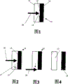
Fig. 1 schematically shows and utilizes laser emission heating (Al, Ga, In) N-substrate interface;
Template/(In) (Fig. 2 and 3) forms sacrifice template and self-supporting (Al, Ga, In) the N single-chip (Fig. 4) of separation to its emission laser to the bottom at the top of N composite article for Al, Ga from sacrificing for Fig. 2-4 expression;
Fig. 5 sacrifices template/(Al, Ga, In) vertical view of N composite article;
Fig. 6 be Fig. 5 the sacrifice template/(In) the N composite article is at the scan laser irradiation corresponding views of operating period for Al, Ga, and wherein laser beam back and forth passes on goods, make and sacrifice template and (Al, Ga, In) N material generation interfacial separation, and obtain (Al, Ga, In) N wafer goods;
Fig. 7 be Fig. 6 the sacrifice template/(Al, Ga, the In) corresponding views of N composite article during peripheral laser radiation operation, wherein laser beam changes circus movement into, from the periphery of goods, carries out radiation continuously with the circle of stair-stepping reduced;
Fig. 8 schematically show sacrifice template/intermediate layer/(Al, Ga, In) N composite article, wherein the laser energy of Chong Jiing is absorbed by the intermediate layer and makes its decomposition, and with the sacrificial mold flaggy with (In) the N layer separates for Al, Ga;
Fig. 9 schematically show sacrifice template/intermediate layer/(Al, Ga, In) N composite article, the laser energy that absorb to impact of intermediate layer wherein, make near it (In) N material degeneration will be sacrificed template and (Al, Ga, In) N gas producing formation separation for Al, Ga;
Figure 10 schematically show by HVPE growth (Al, Ga, In) N and from sacrificing template/(In) the N composite article back side (passing template) is with the equipment of Laser emission to the composite article for Al, Ga;
Figure 11 schematically shows part growth and the piece-rate system of using the cover plate on the chip support.
Detailed Description Of The Invention and preferred embodiment
The content of following United States Patent (USP) and U.S. Patent application is quoted its full content separately as a reference at this:
U.S. Patent application No.08/188,469, the applying date is on January 27th, 1994, and the invention people is people such as Michael A.Tischler, and existing the mandate is United States Patent (USP) 5,679,152;
U.S. Patent application No.08/955,168, the applying date is on October 21st, 1997, the invention people is people such as Michael A.Tischler;
U.S. Patent application No.08/984,473, the applying date is on December 3rd, 1997, and the invention people is people such as Robert P.Vaudo, and existing the mandate is United States Patent (USP) 6,156,581;
U.S. Patent application No.09/179,049, the applying date is on October 26th, 1998, the invention people is people such as Robert P.Vaudo;
U.S. Patent application No.09/524,062, the applying date is on March 13rd, 2000, the invention people is people such as Robert P.Vaudo;
U.S. Patent application No.09/605,195, the applying date is on June 28th, 2000, the invention people is people such as Jeffrey S.Flynn;
U.S. Patent application No.09/929,789, the applying date is August 14 calendar year 2001, the invention people is people such as Michael A.Tischler; And
U.S. Patent application No.09/933,943, the applying date is August 21 calendar year 2001, the invention people is people such as Michael A.Tischler.
One aspect of the present invention relates to the preparation self-supporting, and (In) method of N material comprises for Al, Ga: provide extension compatible sacrifice template; On template, deposit monocrystalline (Al, Ga, In) N material; And by (In) interface modification of N-template will be sacrificed template and (Al, Ga, In) N material separation for Al, Ga.
Interface modification can be with a lot of any carrying out that are fit in the mode, for example, by at (Al, Ga, In) the N material cooled heated (Al, Ga, In) N-substrate interface before environment temperature, by the laser beam impinge interface, the intermediate layer that is easy to separate by use is by the decomposition with boundary material, by produce gas on the interface, by sound irradiation interface, by electron beam irradiation interface, by the rf coupling at interface, by corroding, selectivity reduction by boundary material is perhaps by other optics, acoustics, physics, chemistry, heat or energy process.Acoustic treatment can comprise the acoustic energy that is directly delivered on the interface, and the boundary material on the interface preferably is easy to separate, for example, and by means of special acoustic energy absorption-type intermediate layer.Chemical treatment can comprise the light degradation of boundary material, for example places the light-sensitive material on the interface, discharges free radical with the decomposition reaction of catalysis interface under the optical excitation condition; Or chemical erosion, wherein boundary material preferably is subject to be input to sacrifice template/(Al, Ga, In) erosion of the aggressive agent in the environment of N composite article.For one of ordinary skill in the art, after the content below reading, will sacrifice template/(Al, Ga, In) sacrifice template in the N composite article and (In) several different methods of N material separation will become apparent for Al, Ga.
In the method for the invention, (Al, Ga, In) deposition of N can be undertaken by any suitable method, comprise hydride gas phase epitaxial growth (HVPE), metallic organics gaseous phase extended growth (MOVPE), chemical vapor deposition (CVD) and molecular beam epitaxial growth (MBE), but be not limited thereto.United States Patent (USP) 5,679,152, United States Patent (USP) 6,156,581, U.S. Patent application No.09/179,049 and U.S. Patent application No.09/524,062 has described preparation (Al, Ga, the In) method of N monocrystal material, the oneself that its thickness is enough to reach after separating from template supports (being self-supporting) degree.
(In) the N goods are suitable for use as matrix to the self-supporting of the inventive method preparation for Al, Ga, are used to prepare the precursor structure of microelectronics and/or photoelectron device or device.Self-supporting of the present invention (Al, Ga, In) the N goods have three-dimensional (x, y, z) feature, in one embodiment of the invention, x, each size of y direction is at least 100 microns, the z direction is at least 1 μ m.In another preferred embodiment of the present invention, (In) the N goods are columniform or discoidal to the monocrystalline self-supporting for Al, Ga, and its diameter is that d and thickness are z, and wherein d is at least 100 μ m, and z is at least 1 μ m.In a particularly preferred embodiment, each d and z size are at least 200 μ m.In yet another embodiment, (In) the thickness z of N goods is at least 100 microns to the monocrystalline self-supporting for Al, Ga, and diameter is at least 2.5 centimetres.
As what discuss in the background parts, a special advantage removing expendable material before being cooled to environment temperature is defective and the crackle of having avoided the TCE difference to cause.In order at utmost to bring into play this advantage, growth temperature ± to carry out lock out operation within 300 ℃ be favourable.But separation temperature also can be controlled at growth temperature, than low temperature of growth temperature or the temperature higher than growth temperature, so that handle the TCE difference, makes the thermal stress in the material reach minimum level (or control).Other condition of growth course (for example, pressure) can optionally be controlled at separating step, and one of ordinary skill in the art can be rightly according to the content here and easily determined these.
In separation process, (In) among the N, (In) the N-substrate interface is locally heated the decomposition that causes a kind of material for Al, Ga, causes (the separation of mould material and (Al, Ga, In) N material) of two kinds of materials for Al, Ga.
(In) method for optimizing of N-substrate interface is to use the laser irradiation, as schematically showing of Fig. 1 for Al, Ga in heating.Composite construction 10 comprises sacrifices template 12, and (In) N material 16 is grown in the above for Al, Ga, mould material and (Al, Ga, In) formation interface 14 between the N material.Coherent beam 20 for example, is produced by Nd:YAG laser (not shown among Fig. 1), and it is propagated to see through and sacrifices template 12, and to sacrifice template 12 be printing opacity for selected laser irradiation; Impact then (Al, Ga, In) N material, and (In) (the 3rd harmonic wave of Nd:YAG (355nm) is only absorbed by the AlGaInN material N material, and approximately Eg<3.49eV) 14 impact zone 18 is lighttight at the interface for selected laser for Al, Ga.With sacrifice template lighttight at the interface (In) laser energy that absorbs in the N material causes the chemistry and/or the physical change of material at the interface for Al, Ga.The degradation effects of the boundary material that is caused is sacrificed template and (Al, Ga, In) separation of N material.
In an illustrative embodiment, to sacrifice template and make by sapphire, the high energy laser beam of enough light beam power density directly penetrated sapphire and at (Al, Ga In) absorbs in the N material, makes (Al, Ga, In) produce thermal decomposition in the thin boundary layer of N, thus (Al, Ga, In) N separates with template, become self-supporting (Al, Ga, In) N crystal.In this embodiment, the energy of light source greater than (Al, Ga, the In) band gap of N material, thus can be absorbed effectively; But less than the band gap of sapphire, thereby light transmission sapphire.For example, the 3rd harmonic wave of Nd:YAG laser (355nm) is suitable for GaN-sapphire system, 1000 ℃ separation threshold values greater than 150mJ/cm
2The threshold value of laser energy (causing that thermal decomposition or other physics and/or chemical degradation change) depends on several factors, comprise beam size and Energy distribution, the laser energy of wavelength and absorption, but the decomposition temperature of temperature of separating and decomposing material, but be not limited thereto.
Make (In) N and template layer reach and fully separate the useful laser beam principal character that is adopted and be for Al, Ga:
(i) photon energy of laser is bigger, greater than (Al, Ga, In) N and sacrifice the band gap of one of mould material, and less than the band gap of another kind of material;
(ii) the power density of laser is enough high, can cause the chemistry and/or the physical change of boundary material, sacrifices template and (Al, Ga, In) interface binding power between the N material thereby can weaken at least;
The (iii) short pulse of used irradiation, reduce to enter the thermal diffusion depth (beyond the interface) of material, reduce shock wave by the laser energy generation that absorbs, and usually reduce (the Al that obtains, Ga, In) physics and/or chemical change amount in the N material, thereby with monocrystalline (Al, Ga, In) damage of N product material is reduced to minimum level;
(iv) with the pulse of used irradiation, and used illumination beam template/(In) selective scanning one on the N composite article works for Al, Ga, and utilization is the pulsation rate in isolation of crystalline district effectively sacrificing; And
(although v) most beam profile can be used (Gaussian (Gaussein), most solemn of ceremonies shape for hat (Top Hat), or the like), uniformly, cylinder symmetric and the beam profile from high-energy to low-yield transition gradually be desired.
Except beam profile, used beam quality good more (better calibration and near desirable Gaussian beam profile), light beam can keep the time of suitable shape long more during motion before reaching sample passing optics or part.This factor is important, for example, if must maybe need to position the laser over from the growth reactor larger distance or use a laser cell to adapt to multiple (Al, Ga, In) N growth room (reactor).Template/(In) beam homogenizer of N composite article (wafer) or scattering physical efficiency are used to make the beam profile edge not special for Al, Ga near sacrificing.The coarse machined surface at the quartz of roughening or the template back side can be used to realize the selective light beam uniformity of laser irradiation energy, and above-mentioned laser irradiation energy is to focus on that the sacrifice template/(Al, Ga is In) on the N composite article.
In order to isolate the area bigger than beam diameter, laser beam can cross that the sacrifice template/(In) N composite article scanning is shown in Fig. 2,3 and 4 for Al, Ga.
By providing passage, the sacrifice template that makes it to overflow/(Al, Ga, In) N composite article, thereby realization scanning well for the gas (boundary material decomposition generation is that the result who produces is impacted in used irradiation) that discharges.(In) thermal decomposition of N will discharge the N as cleavage reaction product for Al, Ga under used laser energy
2But, N
2Be trapped on the interface, will cause the unequal stress that cracks.Therefore, scanning is preferably from the edge of wafer, and inwardly motion gradually, thereby makes the N of release
2Overflow easily.
Fig. 2 represent to sacrifice template/(In) the N composite article 10 for Al, Ga, and wherein coherent beam 20 sees through and sacrifices template 12 transmission, move along being directed downwards shown in the arrow A from the top of goods 10, thereby impact zone 18 decomposing shape grooving.Along with light beam 20 moves to interface 14, as the N of catabolite
2Groove by impact zone 18 is overflowed and is sacrificed that template/(In) the N goods 10 for Al, Ga.
Fig. 3 represents to sacrifice template/(Al, Ga, In) the N goods 10, and this moment, its motion of coherent beam 20 end arrived the bottom margin of goods, finish the decomposition at interface 14, to sacrifice template 12 and (In) N layer 16 separately for Al, Ga, thereby make the latter form self-supporting (Al, Ga, In) N wafer product, as shown in Figure 4.
Sacrifice template and (In) between N material separation period, the scintigram of laser beam comprises that laser beam is along the translation that is suitable for the predetermined figure of lock out operation for Al, Ga in shock effect.For example, laser beam front and back scanning easily, and/or along circular motion (this is a circular diagram for most of wafers).Finishing of scanning is by mobile wafer physically, by the deflection laser bundle, or the combination of the two.Template/(In) in the pulsed laser irradiation at N interface, the step size between the laser pulse can be from 1 to 200% of beam spot size on the interface for Al, Ga, but more preferably from separating 10 to 50% of beam spot size more than the threshold value sacrificing.
Although by in that (In) the N material is carried out separation by laser near sacrificing the temperature of growing on the template for Al, Ga, make strain be reduced to minimum level, but in broad practice of the present invention, also can be lower than execution separation by laser operation under the lower temperature of growth temperature, for example, at ambient temperature.Irradiation sacrifice template under the temperature of growth temperature/(In) N interface makes template and (In) the N material separates for Al, Ga, because along (In) laser scanning of N crystal face has reduced the crackle that overstrain causes for Al, Ga for Al, Ga because being starkly lower than.This scanning along crystal face at high temperature may be important, but more important when complex is in condition under the stress.
As an example, the c face GaN that grows on c face sapphire is when sacrificing template/(Al, Ga, In) N goods cool to room temperature and be heated near the growth temperature temperature again when carrying out separation by laser is along GaN<1120〉incidence and the degree of face scanning minimizing crackle.Generally need be parallel to (Al, Ga, In) the low index face scanning in a face of N or edge.
Although beam flying is useful, cover sample if can obtain having the laser of enough big beam sizes and power density, just can use light beam pulse to separate separately to whole sample.
Fig. 5 sacrifices template/(Al, Ga, In) vertical view of N goods 30.
Fig. 6 is that the sacrifice template/(In) the N composite article is at the scan laser irradiation corresponding views of operating period for Al, Ga, and wherein laser beam back and forth passes on goods, make and sacrifice template and (Al, Ga, In) N material generation interfacial separation, and obtain (Al, Ga, In) N wafer goods.
Fig. 7 be sacrifice template/(Al, Ga, the In) corresponding views of N composite article during the circumference laser radiation operation, wherein laser beam, carries out with the circular arc of stair-stepping reduced, as shown in the figure from the periphery of goods 30 continuously along circular motion.
Separation by laser process need laser arrives (Al, Ga, In) interface between N and the mould material.In order to reach this purpose, the laser irradiation must be passed (Al, Ga, In) in N and the mould material, and by another absorption in these materials.For (Al, Ga, In) N growth, the character of sacrificing template is depended in the path of laser irradiation.
For example, if template is the material such as sapphire, have than (Al, Ga, In) the big band gap of N, laser beam can penetrate sapphire (being called the material back layer, because this " side " is " back side " or supporting layer in growth course), (In) the N material absorbs laser beam for Al, Ga.
But, when template have than (Al, when Ga, band gap that In) N is low (for example, Si, GaAs, SiC, InP, low band-gap (Al, Ga, In) N etc.), laser beam can penetrate (Al, Ga, In) N material and sacrificed template and absorb.The light that absorbs produces heating, makes a kind of material production chemical change.Usually, have than (template of the band gap energy that In) the N material is big is the irradiated back side for Al, Ga.The expository material of constitute sacrificing template comprise sapphire, big band gap (Al, Ga, In) N, spinelle, or the like, but be not limited thereto.
In addition, in that (Al, Ga In) can use one or more intermediate layers to absorb light on the N/ substrate interface.The suitable material in this intermediate layer comprises those because adjacent layer heats and the material of easier decomposition, and raising or promotion (Al, Ga, the In) material of N growth, perhaps the two is comprehensive.If the adopts band crack is than (Al, Ga, the laser energy absorption layer that In) N layer and template are little, laser can penetrate sacrifice template/(Al, Ga, In) any surface of N composite article.For example, 10 microns InGaN layer of growth on the sapphire surface, then the GaN layer of grow thick on the InGaN layer.Be easy in the InGaN layer, absorb to be used to make the light of InGaN layer generation chemistry or physical change, also penetrate GaN or sapphire layers easily.
By serious doping (In) N layer reduces band gap effectively, also can form the intermediate layer for Al, Ga.For example, can use adulterant Si, O or Ge to form (Al, Ga, In) N layer, the irradiation of easier absorption incident that tangible n type mixes.In addition, adulterant Mg, Zn, Be be can use, (Al, Ga, In) N layer, easier absorption incident radiation that obvious p type mixes formed.For this purpose, concentration of dopant surpasses 1 * 10
18Cm
-3Be preferred.The height defect area is for example found among the GaN on sapphire, and band gap is reduced.
The rear side of irradiated template or front side can be uniformly, and perhaps they also can be to form pattern, thereby allow the separation by laser in the specific region.Sacrifice template and form pattern or use the intermediate layer that forms pattern can be used for for example reaching horizontal extension undue growth (LEO), this perhaps is convenient to slippage or cracking on preferred orientations as a technology that reduces defective.
Select the intermediate layer, for example, they can optionally be corroded or decompose, with will grow (In) N separates with the sacrifice template for Al, Ga.In addition, can select the intermediate layer to be connected to thermal source or opposite, so that help to separate (Al, Ga, In) chemistry of N material or physical change mode.
For example, Fig. 8 schematically shows that the sacrifice template/(In) N composite article is comprising sacrificial mold flaggy 38 with (In) the N layer 42 for Al, Ga, and the two is separated by intermediate layer 40 for Al, Ga.Laser beam 36 shines on the intermediate layer, and the intermediate layer is decomposed, and with sacrificial mold flaggy 38 and (Al, Ga, In) N layer 42 separation.
Fig. 9 schematically shows that the sacrifice template/(In) N composite article is comprising sacrificial mold flaggy 38 with (In) the N layer 42 for Al, Ga, and the two is separated by intermediate layer 40 for Al, Ga.The laser beam 36 that shines on the intermediate layer is absorbed by the intermediate layer.But in this embodiment, the laser beam energy that the intermediate layer absorbs causes near (Al, Ga, In) the N material breakdown the intermediate layer.It is this that (In) decomposition of N material makes sacrificial mold flaggy 38 and (Al, Ga, In) N layer 42 separation for Al, Ga.
In separation process, need light beam irradiates arrive (Al, Ga, In) on the N-substrate interface, this means laser must according to mould material and laser from sacrifice template/(Al, Ga, In) the N composite article (In) N one side or template one side shine on the interface for Al, Ga.Therefore need to select the mould material that is used to separate and laser energy to make and pass sacrifice template/(Al, Ga, In) template of N composite article (is sacrificed template/(Al, Ga, In) N composite article) or is passed (Al from the irradiation of template one side, Ga, In) the N material is (from (In) template/(Al is sacrificed in the irradiation of N one side for Al, Ga, Ga, In) N composite article) the not obvious obstruction of laser beam passway (absorb or reflection) light beam.For example, if adopt the irradiation of UV laser sacrifice template/(Al, Ga, In) template one side of N composite article, the UV irradiation that then needs template to produce for laser is the height printing opacity.
Laser beam passway passes through surrounding environment, i.e. the laser beam of Chan Shenging and sacrifice template/(Al, Ga, In) environment between the N composite article also must be considered, has suitable feature (intensity) to guarantee the light beam that shines on the goods, make template and (Al, Ga, In) N separation.And the incidence angle of laser beam can not be too little, so that light beam is reflected by interference surface.
In an illustrative embodiment, adopt UV laser, template/(In) useful UV suprasil is directly adopted at the back side of N composite article for Al, Ga, and propagation UV laser shines sacrificing.In addition, can use sapphire, AlN or other only material transparent, but these materials must be compatible with its position in growth room (reactor) to being used to separate.For example, sacrifice template/(Al, Ga, In) the N composite article can be placed in the hvpe reactor device, and can be exposed in the corrosive gas and high temperature under, so mould material must with the reactor environmentally compatible (for example, be kept for supporting (the Al of growth in the above, Ga, the In) structural strength of N material, and the transmissivity that acts directly on the irradiation energy of composite article boundary zone).
Figure 10 schematically shows the original position laser separation apparatus, be used for by HVPE guiding (Al, Ga, In) the N growth and from the composite article back side (passing template) template/(Al, Ga is In) on the N composite article to sacrifice with Laser emission.
In the system of Figure 10, laser 50 comes with ripple plate 52 and polarizer 54, is used for energy modulation, with the irradiation of the suitable feature that is provided for separating.Laser beam is expressed as big schematic arrow in Figure 10.By mirror 56 and relevant energy meter 58 can measuring beam energy, this only uses in the energy measurement process.Therefore energy measurement can be used for characterizing laser beam, thereby adopts the position/setting of suitable ripple plate 52 and polarizer 54 to be used for the energy modulation.
Laser beam shines mirror 62 and reflexes to x-y scanner 60 in the normal running between separation period.The optionally mobile laser beam of x-y scanner 60 guides it to arrive mirror 64, passes thus and is contained in (Al, Ga, In) pedestal 68 in the N growth reactor 66.The composite crystal goods are placed on the pedestal 68, and be included in sacrifice growth on the template 72 (In) the N layer 70 for Al, Ga.
Sacrifice template and can see through laser beam, thereby the light beam that passes pedestal 68 shines sacrifice template/(Al, Ga, In) N interface by sacrificing template 72.Absorb laser energy at the interface, make and sacrifice template 72 and (In) the N material separates, and obtains self-supporting (Al, Ga, In) (Al, Ga, In) the N material of N single crystal articles form for Al, Ga.
Above-mentioned HVPE can be made and be arranged to carry out to growth reactor 66, perhaps in addition, also can use and be other (Al, Ga, In) growth reactor of preparation of N growth technique and layout for example, is used to carry out MOVPE, CVD, MBE or is used for deposition/growth (Al on matrix, Ga, In) method well known in the art or the technology of N material.
Utilize x-y scanner 60 to scan in the system of Figure 10, the passage of laser beam is not in that the sacrifice template of pedestal 68/(In) entire cross section of N composite article has obstacle on long-pending for Al, Ga.Therefore this also needs pedestal to have suitably big cross-sectional area, thus whole (Al, Ga, In) the N vitellarium that form on the inswept template of light beam energy.In addition, the sacrifice template on the pedestal/(In) the N composite article can rotate and move for Al, Ga, make (Al, Ga, In) whole growth of N material distinguish from.Also comprehensively laser deflection and movement of wafers (for example, are sacrificed template/(In) the N composite article can be rotated for Al, Ga, and laser beam deflection is from the boundary scan to the center).In order to control the loss of heat, can place one or more transparent baffles in the pedestal lower end from the big base opening part.
Since with pedestal 68 as sacrifice template/(Al, Ga, the In) supporting construction of N composite article, therefore preferably pedestal 68 has high-permeability for laser beam.For ultraviolet laser, for example, pedestal can be made by the UV suprasil, makes light be penetrated into sacrifice template/(Al, Ga, In) N composite article.In order to become the non-absorbent of incident laser irradiation, this quartz material is preferably bubble-free and contain minimum particle.It is transparent also can adopting other the irradiation for UV, perhaps is the manufactured materials (for example sapphire, AlN or the like) of high permeability at least.For the irradiation of the laser of other type (as, infrared, xenon, excimers, CO
2Deng), be used to make the suitable material of pedestal, be easy to determine for persons skilled in the art.
Template/(Al, Ga In) use the other advantage of transparent backing material to be in the N composite article sacrificing, (Al, Ga In) can directly monitor growth course during the N to deposition on the sacrifice template, by feed back control system and technology, this supervision can be used to control growth course.This feedback closed loop processing ease is implemented, as (Al, Ga, In) part of the whole technology controlling and process subsystem in N growth and the original position piece-rate system.
The surface of pedestal or other reactor wall material, perhaps or even sacrifice that template/(In) the sacrificial mold backboard face of N composite article be made its shape adapt to sacrifice template/(Al, Ga, In) light beam on the N interface that shines composite article after can being modified for Al, Ga.For example, these surfaces can roughening, makes the incident beam diffuse scattering, perhaps makes their shape become a series of lenticule, is convenient to the focusing of special area, perhaps they can be decorated, and prevents the luminous of some zone.
In that (Al, Ga In) in the assembling of N growth and piece-rate system, must very carefully carry out optics and select and move, thereby make them compatible with optical maser wavelength, and make and sacrifice template and (Al, Ga In) reflect minimum in the operating process disconnected from each other of N material.They preferably should make reflection minimum, because can cause the interference or the negative variation of beam profile.As a kind of part release tech, to interfere the edge also can be used to carry out and separate with light belt one, this will go through below.
In that (In) in N growth and the piece-rate system, growth reactor has the suitable construction of using the material compatible with growing environment to make for Al, Ga, and for example, growing environment can comprise that temperature reaches 1200 ℃ growth conditions, such as NH
3, vapor-phase reactant such as HCl and GaCl existence, and can be subatmospheric, be higher than atmospheric or equal atmospheric different pressures size.
When using back side illuminaton to carry out lock out operation, (Al, Ga, In) the N template of growing in the above must be transparent for the laser irradiation, as previously mentioned, and template and composite crystal product support (as, pedestal and use therein any wafer are installed or locating element) must remain no laser absorption deposition, (In) N is the same for Al, Ga as the back side.
Employing prevents that the whole bag of tricks of backside deposition from being favourable.
For example, the system that schematically shows among Figure 10 is designed so that wafer rests on same position and grows and the template removal.The variations in temperature that this layout will be grown and template is removed between the operation is reduced to minimum level.The enforcement of growth and template removal processes also can pass through sacrificing growth on the template in one or more chambers of reactor or part (In) N layer is transported to independent template with the composite crystal goods that obtain and removes chamber or zone for Al, Ga.The composite crystal goods can heat in the process of transporting, so that reduce variations in temperature.
Template is removed the enforcement of operation and can be carried out according to the corresponding manner of above-mentioned back side illuminaton method, laser is shone sacrifice template/(Al, Ga, In) N composite article front, wherein use suitable laser (and wavelength of laser irradiation energy), for example, make the laser beam irradiation pass (Al, Ga, In) N and thermal decomposition intermediate layer or template.
As the method for another kind execution separating step, can grow has several different boundary layer of different chemical metering than (and corresponding different band gap), separates several layers to use tunable laser.
As mentioned above, the back side of template and composite crystal product support preferably keep not having the laser absorption deposition, and in implementation process of the present invention, prevent that the side of composite article and the deposition at top surface edge from also being favourable, so that the LILO process.If (In) same gas of N material arrives the back side and the reaction of sacrificing template to deposition for Al, Ga, and the deposition of generation will prevent that laser beam from arriving separating interface.Be reduced to minimum level for fear of this negative effect and with backside deposition, can adopt following method.
In a method, utilize vacuum, electrostatic force or other not to hinder or the device or the technology of the laser irradiation that seriously decays, can be from the back side with the clamping securely of composite crystal goods, the composite crystal goods enough are clamped on the flat composite crystal product support securely, contact with sacrificial mold backboard face to stop growth gasses stream.
As another method, can make the reaction of growth gasses with the sacrificial mold backboard face in the inert gas purge composite crystal goods away from the back side of sacrificing template or the prevention back side.
Another is at method, material such as borosilicate glass, irradiation is transparent for laser for it, remove under the temperature in growth and template softening or melt, can not remove important impurity gas or with the gas reaction of growth course, can be used to seal the back side, (for example make it not contact growth course gas, the source reactant gas, the product gas of growth course, and gas such as any relevant carrier, diluent).Can provide suitable glass by the composite crystal shape of products, perhaps the growth before with vitreous coating at sacrificial mold backboard face.Glass material also can be used to change stress, and can correspondingly select the glass of special TCE, and stress is reduced to minimum level, or introduces suitable stress in the composite crystal goods.Glass material can be used to cover whole sacrificial mold backboard face, and perhaps they can be used to cover the periphery of sacrificing template, thereby as sealing.
In preventing the other distinct methods of backside deposition, the back side and the composite crystal product support of sacrificing template can apply the material that stops deposition, for example, utilize the chemical vapour deposition (CVD) (PECVD) of sputter, evaporation or plasma strengthening to apply SiO
2Or Si
3N
4Be reduced to minimum level by one or more growth gasses elements are adsorbed onto the surface of solids, undesirable deposition can be reduced to minimum level.In addition, before separating, can remove barrier layer (for example, corroding or other technology removal growth barrier layer), thereby remove any deposition that can exist simultaneously by original position.
As another method that backside deposition is reduced to minimum level, can place the physical barrier of growth gasses stream at the edge of sacrificing template and composite crystal goods, be used for the passage of barrier gas, and will do not need the deposition in zone to be reduced to minimum level.For example, can use cover plate, it has opening, is grown in composite crystal goods front, but the obvious growth that stops the composite crystal goods back side to produce.Favourable formation and layout cover plate make laser arrive the interface of vitellarium, and the gas that produces in the lock out operation is discharged.For example, on the cover board can form groove, provide passage for gas discharges.
What have advantage is, the cover plate among embodiment is taper, and being used for provides occlusion effect and be used to reduce (Al, Ga, In) N deposition on the cover plate in growth course.
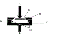
Figure 11 is shown schematically in part growth and the piece-rate system of using cover plate 80 on the chip support 82.Sacrifice template 84 and place on the chip support 82, by delivery source gas in the air-flow shown in the arrow G among Figure 11, (In) N material 86 is grown on the sacrifice template for Al, Ga.Cover plate 80 is tapers, as shown in the figure, makes the locate mode of the deposition 88 of the sorbing material that produces in the growth course be, does not disturb laser energy to be transferred to and sacrifice template 84 and (Al, Ga, In) interface between the N material of growing on template.By this arrangement, the laser beam shown in the arrow L does not have the disturbed template of just passing to shine on the interface among Figure 11.Thereby cover plate has stopped the negative growth result of template, and the conical surface that cover plate begins from open top (channel shape of expansion downwards) is with (In) the N material is reduced to minimum level to the combination of cover plate for Al, Ga.
Now detailed consideration is sacrificed template, the top surface of template, and perhaps relevant with template edge covers the surface, and the mode of its shaping is, helps gas and overflow in separation process, and the while also stops the growth on the template surface.A kind of mode that achieves this end is, at template surface marginal deposit one deck SiO
2, then at SiO
2Form pattern on the layer mould material is exposed, thereby form groove.If shape is enough bigger than (depth-width ratio of groove), will forms seldom or not in the groove and form (Al, Ga, In) N.For example, the layout of groove can be to form series of radial, helps gas and overflows from interface zone.In addition, when forming channel patterns, can make groove branch, so that gas discharges in the separation process.
In the identical device that produces growth, carry out separation process, can reach stronger flexibility when making lock out operation, and be convenient to control the local environment of carrying out lock out operation.
(Al, Ga In) separate under the temperature of N material breakdown temperature (for example, GaN is 800 ℃), can produce and keep cracking nitrogen (for example, atom N or NH in the local environment in separation process if surpassing
3), be used to protect composite crystal goods front that thermal decomposition does not take place.In the local environment of separation process, can add HCl, help on the interface to remove after the decomposition reaction remaining III family element.
In lock out operation, decomposition can occur in the composite crystal goods back side, and stops light to arrive the interface.In this case, can adopt continuous laser operation and corrode the passage that leads to the interface with removing with HCl.In addition, can be such as N
2Isolating environment suitably appears in the environment of atmosphere.
In some cases, if successfully separate in the zone of finding metal, it is favourable keeping the III family metal of interface decomposition reaction generation.Metal will prevent that interface zone from further being damaged by strong illumination from separate areas reflector laser.By monitoring from the light of reflecting surface reflection, can the monitors transmitted progress.
The pressure of carrying out in the equipment that separates can be controlled, so that the stress of equilibrium separation process.For example, carry out the indoor subatmospheric condition of separating, help gas to overflow from separating interface.Usually, from about 10
-6Torr is to about 10
10The pressure of Torr scope is compatible with separation process, and is preferred.Higher pressure can need higher separation temperature (stronger heating or laser energy).In one embodiment, the local pressure in the lock out operation can be>1000Torr, particularly when growth course is carried out under high pressure.
(In) thickness of N material and template layer can be regulated for Al, Ga, makes to comprise template and (In) stress in the composite crystal goods of N material reaches minimum for Al, Ga.Stress be present in usually under the growth temperature (Al, Ga, In) in the N-template system, this be because film have different material characters with template.Usually, thin sacrifice template stress defective and crackle occur than thick-layer is easier, because the relative stress that accumulates in the thin layer will cause crackle, so that discharge stress.Thicker sacrifice template is easier to slight curvature to reuse.
As for (In) thickness of N material lacks balance of existence between rigidity and the intensity in big thickness stress increase and little thickness for Al, Ga.(Al, Ga, In) stress that exists in the N-template system will with (Al, Ga, the In) increase of N thickness and increasing, reason has multiple factor, comprises that material property changes with the increase of leaving the template distance.The easier processing of uncracked thick film and keep its shape and do not damage.
(In) the self-supporting performance of N material is relevant with the area of self-supporting material for Al, Ga for product.It is large-area that (In) the N goods need relatively large thickness to realize self-supporting for Al, Ga.Usually, when (when " heterogeneous " was meant with (Al, Ga, In) N product material difference) last growth here, (In) quality of materials of N improved with the increase of thickness product for Al, Ga in heterogeneous template.For example, be 2 for diameter " the product wafer that separates fully, need that (In) thickness of N material before separation surpasses 50 μ m for Al, Ga.But thin film can partly separate, thereby part is supported by the sacrifice template.If, being cooled to the thermal stress of environment temperature (for example, room temperature) generation less than 50% of the gross area, unsegregated area can finish separation process.
Can sacrifice also that template/(In) N composite article forms the reduction interface of being convenient to separate for Al, Ga by (for example, below<5 ℃) local heat under temperature a little less than heat decomposition temperature (threshold temperature).
In addition, can sacrifice template by chemistry or physical removal after growth assists to separate.To separate that (In) N combines mutually also within the scope of the invention with the distinct methods of sacrificing mould material, for example, combines with chemical erosion by separation by laser, perhaps other combination of heat/physical/chemical step for Al, Ga.
Separation process can change with respect to the time of growth course, made quality of materials reach best, the stress that produces in the management material, and improve (Al, Ga, In) manufacturing capacity of N self-supporting mono-crystal product.Independent in order to make (Al, Ga, In) N wafer, separation process can (Al, Ga In) carry out behind the N growth ending, for example, when sacrificing grow on the matrix 100 to 1000 μ m (Al, Ga is In) after the N.Separation can carried out behind the growth ending or in growth course.
In growth course, carry out the flexibility that separates process can be changed, for example, in (Al, Ga, part parting material when In) N thickness is extremely thin, then continued growth.The part separation energy makes enough materials keep in growth course supporting that (Al, Ga In) the N material time, help stress release.Because laser shines the thermal decomposition that produces and discharges gas decomposition product at the interface, utilize low laser power density to carry out part and separate, will reduce the gas generation and reduce crackle.Part separate (In) N can be behind growth ending for Al, Ga, by further separation by laser, by the not fracture of parting material or by other heat, machinery and/or chemical method that is fit in the cooling procedure, reaches fully and removes.
In addition, when (Al, Ga when In) N thickness is greater than 20 μ m, can all separate in a little zone.Also can adopt subsequently heating (or laser operations) to finish to separate, perhaps when further growth makes (Al, Ga, In) N adhere again on the template or the reactor part on the time carry out parting material once more.
In growth course and/or after the growth course, can repeat the thermal release process once arrives repeatedly, as mentioned above, can use HCl or other reagent that is fit to remove the element (Al of residue III family that after decomposing, exists, Ga, In), because they can stop that laser further shines template/(Al, Ga is In) on the interface of N goods.
Except separating in the growth course, interruption of growth and carry out lock out operation temporarily.In whole growth-separation alternate steps, this order can repeat one or many.
Because near growth temperature separation has discharged the stress relevant with epitaxial growth, can more easily growing thickness, very large (In) N material product surpasses 1-100mm for Al, Ga.(In) the N goods are processed into single wafer for Al, Ga, and processing procedure sees U.S. Patent application No.09/524 in the carrying out of submitting on March 13rd, 2000,062 for details with self-supporting then.
Usually, it is favourable carrying out separation process when growth reaches about 0.01~100mm, and this depends on required (Al, Ga, In) N product.
Although near growth temperature or growth temperature, containing template/(Al, Ga, In) reactor of N goods be cooled to environment temperature (as, room temperature) before, it is most preferred and favourable carrying out separation process, but also can be at template/(Al, Ga, In) the N goods are cooled to carry out separation process after the environment temperature.
Usually, can be at the execution lock out operation of any suitable temperature, this can easily determine according to this paper disclosure for one of ordinary skill in the art.
Separation process can (In) N carries out under the high temperature of sacrificing the original temperature of growing on the template for Al, Ga being higher than, being lower than, equaling or equal substantially.In order to improve performance, carry out the suitable temperature of separating (Al, Ga, In) the N material 400 ℃ of the growth temperature on the template with interior, 300 ℃ with interior, 250 ℃ with interior, 200 ℃ with interior, 150 ℃ with interior, 100 ℃ with interior, 75 ℃ with interior and 50 ℃ in.Template/(In) advantage of the hot conditions of N composite article is for Al, Ga, avoids TCE stress to small part, obtains unstressed or stressless substantially (Al, Ga, In) N self-supporting goods thereby separate under hot conditions.Thermal decomposition does not take place protection AlGaInN is essential, because for example, can be used to contain the surrounding environment of N.
As mentioned above, wish that harmful light absorption or optical attenuation deposition is not present in that template/(In) shadow surface of N composite article or its edge are because this deposition stray light shines on the goods that need separation by laser for Al, Ga.Preferably by (Al, Ga In) utilize sputter or PECVD SiO in the growth course of N on template
2Or other growth inhibitor is reduced to minimum level with backside deposition.Inhibitor in this case can be removed by chemistry before separating.Remove the growth inhibitor layer and have extra advantage for utilizing it to remove any backside deposition.SiO
2Thickness be preferred greater than 50nm, thickness is most preferred greater than 300nm.
Original position is separated (for example, carry out and separate) in the reactor of carrying out growth course, stop backside deposition and template/(In) marginal deposit of N composite article is favourable for Al, Ga by said method.Also can carry out ex situ and separate, wherein from reactor, take out template/(Al, Ga, In) N composite article, execution separation subsequently then.Ex situ is separated and have been cancelled not stopping the needs of laser beam, and this to be original position separate intrinsic.And adopting ex situ to be separated into use and installing layout provides extra flexibility, with protection template/(Al, Ga, In) N composite article edge and back portion.
Physics or chemical scavenging template after growth/(In) N composite article edge is so that the thick (Al that removes in the composite article marginal growth for Al, Ga, Ga, In) N also can be used as a treatment technology, be used to prevent that attachment region from producing (Al, Ga, In) N goods cracking.The physical technique that is used for this removing undue growth comprises, for example, grinds, cuts or rives along crystal plane, but be not limited thereto.The realization of this undue growth of chemical scavenging can be by corroding (at H
3PO
4Or among the HCl) deposition, the erosion and deposition of perhaps using UV light to assist is carried out, and the UV light that wherein focuses on the specific region has improved the speed and the degree that corrode.
When ex situ is separated, laser energy shone template/(Al, Ga, In) similar with during original position is separated of the laser parameter on the N composite article interface.
Scan pattern is included in that template/(In) edge of N composite article begins scanning for Al, Ga, the release particular importance of gas of generation when separating for ex situ.Because template when ex situ is separated/(In) there are more strain in Al, Ga in the N composite article, and be more important than the scanning of carrying out in the original position separation along the scanning of crystal face.When obtainable laser has enough beam spot sizes and light beam power density when being used to separate All Ranges, it is favourable using single beam to separate, and needn't scan.
Too thin and can not self-supporting (Al, Ga, In) N layer, can be before separating by gravity or be attached on the suitable physical support structure and be supported.
The advantage that ex situ is separated is, arrives template/(Al, Ga, In) front of N composite article and back side easily.Can directly arrive the template that increased the ex situ lock out operation and the selection free degree in intermediate layer.
In position with the ex situ lock out operation in, the intermediate layer that reduces strain and crackle is very useful.The intermediate layer can be put into before template enters growth reactor sacrifices on the template, perhaps also can be in (Al, Ga, In) the N material in-situ applications intermediate layer in the growth room of initiatively growing before the beginning.
In extensive enforcement of the present invention, can adopt being lower than of thin layer MIN/separation of part, form the residual surface artificiality as the seed of growth subsequently.Also can adopt being lower than of thick-layer MIN/separation of part, the interface of chemical erosion reduction then is as a technology that improves output.The gas that discharges from the interface in separation process can make the film cracking, reduces output.Use low power density to reduce the gas burst size, and the possibility that in separation process, reduces the wafer cracking.
After separating, (In) the N goods need cleaning for Al, Ga, the remaining III family metal of removing that the interface decomposable process produces.Under room temperature or high temperature, use acid, for example, HCl or HF, purpose is effective hereto.
For fear of separate or the part after separating to (In) thermal shock of N material needs slow cooling procedure for Al, Ga, and best speed<10 ℃/min is although can adopt cooling faster in order to boost productivity.Be suitable for obtaining to have (the Al of required feature, Ga, In) cooldown rate of N end article is not determined by unsuitable experimentation, but passes through empirical relation, shape characteristic and the (Al of time-temperature schedule, Ga, In) the final service test of N goods is determined easily.
Although the present invention has been carried out basic description according to using induced with laser to separate, but also can use the target interface heating of other form, for example, (for example use heat, sound, electron beam irradiation, rf coupling or multiple photon process, carry out 2 kinds of different wavelength of laser irradiations, perhaps be used in combination aligning laser by the UV overflow, or the like).Multiple photon process has more detailed description in following list of references, for example, referring to: Misawa, Hiroaki; Juodkazis, Saulius; Sun, Hong-Bo; Matsuo, Shigeki; Nishii, Junji, Formation of photoniccrystals by femtosecond laser microfabrication, Proc.SPIE-Int.Soc.Opt.Eng. (2000), 4088 (Laser Precision Microfabrication), 29-32; Kuebler, Stephen M.; Cumpston, Brian H.; Ananthavel, Sundaravel; Barlow, Stephen; Ehrlich, Jeffrey E.; Erskine, L.L.; Heikal, Ahmed A.; McCord-Maughon, D.; Qin, J.; Rockel, H.; Rumi, M.; Marder, S.R.; Perry, J.W., Three-dimensional micro-fabrication using two-photon-activated chemistry, Proc.SPIE-Int.Soc.Opt.Eng. (2000), 3937 (Micro-and Nano-photonicMaterials and Devices), 97-105; Sun, Chi-Kuang; Huang, Yong-Liang; Liang, Jian-Chin; Wang, Jiun-Cheng; Gan, Kian-Giap; Kao, Fu-Jen; Keller, Stacia; Mack, Michael P.; Mishra, Umesh; Denbaars, Steven P., Large near resonance third order nonlinearity in GaN, Opt.QuantumElectron. (2000), 32 (4/5), 619-640; And Neogi, Arup; Yoshida, Haruhiko; Mozume, Teruo; Georgiev, Nikolai; Akiyama, Tomoyuki; Wada, Osamu, Intersubband-transition-induced interband two-photon absorption byfemtosecond optical excitation, Proc.SPIE-Int.Soc.Opt.Eng. (2000), 3940 (Ultrafast Phenomena in Semiconductors IV), 91-97.
Although the heating of local here interface is as a kind of change template/(Al, Ga, In) method of the physics at N composite article interface and chemical property is described, but the present invention extensively constitutes, comprise any device or the method that make the interface that physics or chemical change take place, so that (Al, Ga, In) the N material with sacrifice separating of template.For example, injection technique is injected as ion, is used to produce the zone of reduction fracture when extensive enforcement of the present invention.In addition, heat equably or excite whole sample (be not only and be confined to the interface), but be included in less level heating or excite play the method in the intermediate layer that quilt weakened, also included by the present invention.As another feasibility, utilize to make the interface have more chemically reactive technology or intermediate layer, thereby make the boundary zone be easy to eat away, comprise that template/(Al, Ga In) corrode before the N composite article cool to room temperature, and this is also in broad range of the present invention.
Though described independent (Al, Ga, In) N layer and (Al with intermediate layer, Ga, In) N layer, but the invention is not restricted to this, (In) the N goods also can be included for Al, Ga, perhaps comprise the material of relative goods and epitaxially grown layer, apparatus structure, device precursor, other deposition or the device of making by this material, as long as not getting rid of, they do not adopt interface processing so that template/(Al, Ga, In) template of N composite article and (Al, Ga, In) N partly separates.Above-mentioned layer, structure, precursor and material, can be before or after carry out separating deposition, if as (Al, Ga, In) the N goods final use necessary and/or be suitable for its final use get final product.
In addition, although here with reference to sacrificing (the Al that forms on the template, Ga, In) the N material has carried out basic description to the present invention, but the present invention comprises the foreign peoples's composite structure that has the interface between homophase not or the different kind of material widely, the material that its median surface is easy to excite or be subjected to other modification to make the boundary zone is separated into independent part, comprise and at high temperature to handle to be used for the composite structure of interface modification, complex is become part from interfacial separation, perhaps the related compound material structure of interfacial separation at ambient temperature after high-temperature process and cooling.
The features and advantages of the present invention will completely express by following embodiment more.
Embodiment 1
By HVPE growing GaN on sapphire, and in the growth room near the HVPE growth temperature separation by laser GaN/ sapphire composite article, obtain the thick self-supporting GaN of 400 μ m.
In the method, will sacrifice pack into the growth room of hvpe reactor device of (0001) sapphire wafer.Sapphire is heated to about 1000 ℃, and the surface of sapphire is exposed to GaCl gas and NH
3In the gas 165 minutes.GaCl forms NH by the Ga that HCl flows through fusing
3/ GaCl ratio is 23.
Interrupt GaCl and flow, and be controlled at GaN-sapphire complex near the growth temperature and be under the atmospheric pressure, keep NH
3Flow, be used to protect the GaN surface.
The irradiation that separates of the interface debonding of GaN and sapphire layers produces by Nd:YAG laser.The 3rd harmonic wave of Nd:YAG laser is adjusted to 90mJ, uses laser energy metering instrument and ripple plate-polarizer combination.The laser irradiation sees through quartzy pedestal by UV and the sapphire template arrives GaN-sapphire interface.
Between the light period, the rotation of GaN-sapphire complex, laser beam is the electro-optical modulation, so that light beam from the boundary scan to the center, all comes out up to entire wafer.
GaN and sapphire cool to room temperature.
From the growth room, take out self-supporting GaN and sacrifice sapphire.The self-supporting GaN material thickness that obtains is about 400 μ m, visible transparent and do not have crackle, and dislocation density is less than 10
7Cm
-2, the half-breadth of (0004) twin crystal X ray rocking curve is less than 200arcsec.
Embodiment 2
In this embodiment, by HVPE growing GaN on sapphire, and separation by laser at high temperature, obtain the self-supporting GaN wafer of diameter 40mm.
Carry out following treatment step:
(1) back spatter of (0001) sapphire wafer applies the SiO of 300nm
2The edge of wafer forms some coatings simultaneously, but prevents SiO
2Deposit in the front of wafer (growth side);
(2) growth room of sacrifice (0001) the sapphire wafer load level hvpe reactor device that sputter is applied;
(3) sapphire is heated to about 1000 ℃, the surface of sapphire is exposed to GaCl gas and NH
3In the gas 180 minutes, GaCl formed NH in the method by the Ga that HCl flows through fusing
3/ GaCl ratio is 35;
(4) interrupting GaCl flows;
(5) interrupt NH
3Flow;
(6) from the growth room, take out GaN/ sapphire complex;
(7) after taking out from the growth room, GaN/ sapphire complex keeps at room temperature several days time;
(8) corrode SiO by the comprehensive HF of use
2Several hours and physical grinding are removed the GaN that is deposited on sapphire one side and the GaN-sapphire complex edge;
(9) GaN/ sapphire complex is packed in the vacuum chamber, make the GaN surface be positioned at the SiC grain bed;
(10) 1cm is thick quartz disk is placed on the GaN/ sapphire complex, and the surface (coarse finished surface) that makes its alligatoring is near GaN/ sapphire complex, so that laser beam is even;
(11) vacuum chamber is found time, and charge into N
2Gas;
(12) GaN/ sapphire complex is heated to about 900 ℃;
(13) use laser energy metering instrument and ripple plate-polarizer combination, the 3rd harmonic irradiation of Nd:YAG laser is adjusted to 100mJ, then the laser irradiation is propagated into vacuum chamber, arrive GaN/ sapphire interface by quartz window, quartz disk and sapphire;
(14) with laser beam electro-optical modulation, light beam is shone on wafer, light beam is since an edge, parallel sweep GaN { the 112bar0} face comes out up to the entire wafer zone;
(15) with GaN and sapphire cool to room temperature;
(16) GaN and sapphire are put into the HF solution 30 minutes of dilution, from HF, taken out self-supporting GaN then, and in deionized water, wash;
(17) the GaN material is made the circular wafer of diameter 40mm, an one planar side uses a friction particles to be indicated { 112bar0} direction;
(18) use 9 μ m and 3 μ m boart boarts that wafer is ground to uniform thickness and machine glazed finish;
(19), obtain to carry out the epitaxial growth GaN wafer with the wafer chemical-mechanical polishing.
The about 200 μ m of the self-supporting GaN wafer thickness of the diameter 40mm that finally obtains, visible transparent and do not have crackle, dislocation density about 2 * 10
7Cm
-2, the root mean square surface roughness is less than 1nm.
Though according to difference explanation aspect, feature and embodiment to the description of being illustrated property, but it should be understood that, implementing much to change, to revise when of the present invention and other embodiment also is possible, so the present invention comprises all this variations, modification and other embodiment that spirit and scope of the invention is interior widely.
Claims (24)
1. one kind prepares self-supporting (In) method of N goods comprises the steps: for Al, Ga
Provide extension compatible sacrifice template;
(In) N material is so that formation sacrifice template/(In) N composite article is comprising sacrificing template and (Al, Ga, In) interface between the N material for Al, Ga for Al, Ga to deposit monocrystalline on template; And
To sacrifice template/(In) the N composite article carries out interface modification for Al, Ga, so as will to sacrifice template with (Al, Ga, In) N material separation, and obtain self-supporting (Al, Ga, In) N goods,
Wherein, to sacrifice template/(Al, Ga, one or more during In) the N composite article step of carrying out interface modification comprises the steps:
Energy is confined on the interface;
The interface is heated to a temperature that activates or cause physics or chemical change;
The interface is cooled to be lower than the temperature of growth temperature;
Modification interface aspect energy;
Aspect energy, excite the interface;
The intermediate layer is provided on the interface, wherein can uses the adulterant intermediate layer of arbitrarily mixing;
Produce gas at the interface;
Decompose boundary material;
Impact the interface with acoustic energy;
Impact the interface with the impact media of from following group, selecting: proton, ion and the particle beams;
Arbitrarily impact the interface with laser beam, described laser energy is a pulsed;
Rf is coupled to thermal interface;
Corrode the interface;
Selectivity reduction boundary material; With
Boundary material is carried out light degradation.
2. the method for claim 1, it is characterized in that on template, depositing monocrystalline (In) step of N material comprises the technology of selecting from following group for Al, Ga:
Hydride gas phase epitaxial growth (HVPE);
Metallic organics gaseous phase extended growth (MOVPE);
Chemical vapor deposition (CVD); With
Molecular beam epitaxial growth (MBE).
3. the method for claim 1, (Al, Ga In) in 500 of the temperature of N material step ℃, implement that template/(In) the N composite article carries out the step of interface modification for Al, Ga to sacrificing to it is characterized in that depositing on template monocrystalline.
4. the method for claim 1 is characterized in that template/(In) the N composite article step of carrying out interface modification comprises that the laser energy that is used to from Nd:YAG laser impacts the interface for Al, Ga, and described Wavelength of Laser is near 355nm to sacrificing.
5. the method for claim 1, it is characterized in that sacrificing template/(Al, Ga, In) the N composite article step of carrying out interface modification comprises and utilizes laser energy to impact the interface, and the photon energy that described laser energy has is greater than (Al, Ga, In) N material and sacrifice the band gap of a kind of material in the mould material, and less than the band gap of another kind of material.
6. the method for claim 1, it is characterized in that to sacrifice template/(In) the N composite article step of carrying out interface modification comprises with laser energy and impacts the interface, and described laser energy has the shape of selecting from following group for Al, Ga:
Most solemn of ceremonies shape for hat beam shape;
From have high-octane beam center to have low-energy beam edge uniformly, the intermediate shape of cylinder symmetric.
7. the method for claim 1 is characterized in that sacrificing template and has the quartzy of roughening at its back side or carried out matsurface processing.
8. the method for claim 1, it is characterized in that sacrificing template/(Al, Ga, In) the N composite article step of carrying out interface modification comprises and utilizes laser energy to impact the interface, described laser energy impacts according to predetermined scan pattern, comprise laser beam and/or sacrifice template/(Al, Ga, In) translational motion of N composite article.
9. want 1 described method as right, it is characterized in that template/(In) the N composite article step of carrying out interface modification comprises and utilizes laser energy to impact the interface for Al, Ga to sacrificing, described laser energy is along (Al, Ga, In) the N crystal face impacts according to predetermined scan pattern, wherein (Al, Ga, In) the N material comprises c face GaN, sacrifice template and comprise c face sapphire, and scan pattern comprise along c face GaN { the 11-20} direction scans.
10. the method for claim 1 is characterized in that depositing monocrystalline (Al, Ga on template, In) during the step of N material, utilize the material of from the group that following material constitutes, selecting to sacrifice template/(Al, Ga, In) sealing backside of N composite article: borosilicate glass, SiO
2And Si
3N
4
11. the method for claim 1, it is characterized in that sacrificing template/(Al, Ga, In) the N composite article carries out interface modification, so that will sacrifice template and (Al, Ga, In) the N material separates and obtains self-supporting (Al, Ga, the In) step of N goods is to carry out in the processing environment of input cracking nitrogen or HCl.
12. the method for claim 1, it is characterized in that to sacrifice template/(In) the N composite article carries out the beginning of the step of interface modification for Al, Ga, sacrifice on the template (In) thickness of N material is in the scope of 50 to 1000 μ m for Al, Ga.
13. the method for claim 1, it is characterized in that sacrificing template/(Al, Ga, In) the N composite article carries out interface modification, so that will sacrifice template and (Al, Ga, In) the N material separates and obtains self-supporting (Al, Ga, In) step of N goods, comprise sacrifice template and (Al, Ga, In) the N material partly separates, wherein not the area of separating part less than sacrificing 50% of the template gross area on the interface, and comprise sacrifice template/(Al, Ga, In) the N goods are cooled to environment temperature, sacrifice template and (Al to finish, Ga, In) separation of N material.
14. the method for claim 1, it is characterized in that in that template/(In) the N composite article carries out interface modification for Al, Ga to sacrificing, so that will sacrifice template and (Al, Ga, In) the N material separates and obtains self-supporting (Al, Ga, In) after the step of N goods, (In) the N goods are cooled to environment temperature for Al, Ga with self-supporting.
15. the method for claim 1, it is characterized in that (In) the N goods are cooled to before the environment temperature for Al, Ga in self-supporting, to sacrificing template/(Al, Ga, In) the N composite article carries out interface modification, so that will sacrifice template and (Al, Ga, In) the N material separates and obtains self-supporting (Al, Ga, In) N goods.
16. the method for claim 1 also comprises in the separation process at high temperature, adopts ammonia or other to contain the N material and protects sacrifice template/(Al, Ga, In) preceding flooring of N composite article.
17. the method for claim 1 is characterized in that (In) thickness of N goods is about 1 to 1000 μ m to self-supporting for Al, Ga.
18. the method for claim 1 comprises that also (In) the N goods are made the wafer that thickness is about 100 to 1000 μ m for Al, Ga with self-supporting.
19. the method for claim 1, it is characterized in that sacrificing template and constitute sacrifice template/(Al, Ga, the In) back side template in the N composite article, and utilize the laser energy transmission pass described back side template to carry out laser energy is impacted step on the interface.
20. the method for claim 1 is characterized in that sacrificing that template/(In) backside deposition of N composite article is partly suppressed by the step of selecting at least for Al, Ga: use cover plate in the deposition step process from following group; Utilize the molten glass sealing to sacrifice template; In described deposition step process, use vacuum locate with fixing the sacrifice template/(Al, Ga, In) N composite article, and be not exposed to (Al, Ga is In) under the N material; In described deposition step process, physically fixedly positioning the sacrifice template/(Al, Ga, In) N composite article, and be not exposed to (Al, Ga is In) under the N material; And on the sacrifice template, use coating, to stop deposition at its back side.
21. the method for claim 1 is characterized in that sacrificing that template/(In) the N composite article is being sacrificed template and (Al, Ga In) contain one deck intermediate layer at least between the N material for Al, Ga.
22. the method for claim 1 is characterized in that template with (In) N material separation steps comprises the step of selecting from following group for Al, Ga: at high temperature will sacrifice template and (In) the N material partly separates for Al, Ga; Make interfacial fracture will sacrifice template and (Al, Ga, In) N material separation; And finish at ambient temperature and sacrifice template and (Al, Ga, In) separation of N material.
23. the method for claim 1 also is included in self-supporting (Al, Ga, In) other (Al, Ga, In) N of growth on the N goods.
24. a method for preparing the miniature electronic device comprises the steps:
Provide extension compatible sacrifice template;
(In) N material is so that formation sacrifice template/(In) N composite article is comprising sacrificing template and (Al, Ga, In) interface between the N material for Al, Ga for Al, Ga to deposit monocrystalline on template; And
To sacrifice template/(In) the N composite article carries out interface modification for Al, Ga, so as will to sacrifice template with (Al, Ga, In) N material separation, and obtain self-supporting (Al, Ga, In) N goods,
Wherein, to sacrifice template/(Al, Ga, one or more during In) the N composite article step of carrying out interface modification comprises the steps:
Energy is confined on the interface;
The interface is heated to a temperature that activates or cause physics or chemical change;
The interface is cooled to be lower than the temperature of growth temperature;
Modification interface aspect energy;
Aspect energy, excite the interface;
The intermediate layer is provided on the interface, wherein can uses the adulterant intermediate layer of arbitrarily mixing;
Produce gas at the interface;
Decompose boundary material;
Impact the interface with acoustic energy;
Impact the interface with the impact media of from following group, selecting: proton, ion and the particle beams;
Arbitrarily impact the interface with laser beam, described laser energy is a pulsed;
Rf is coupled to thermal interface;
Corrode the interface;
Selectivity reduction boundary material; With
Boundary material is carried out light degradation; And
Formation comprises described self-supporting (Al, Ga, In) device of N goods or device precursor structure.
Applications Claiming Priority (2)
| Application Number | Priority Date | Filing Date | Title |
|---|---|---|---|
| US09/947,253 US6958093B2 (en) | 1994-01-27 | 2001-09-05 | Free-standing (Al, Ga, In)N and parting method for forming same |
| US09/947,253 | 2001-09-05 |
Related Child Applications (2)
| Application Number | Title | Priority Date | Filing Date |
|---|---|---|---|
| CN2008101301585A Division CN101353813B (en) | 2001-09-05 | 2002-08-12 | Free-standing (Al, Ga, In)N and parting method for forming same |
| CN201110301148.5A Division CN102383193B (en) | 2001-09-05 | 2002-08-12 | Free-standing (Al, Ga, In)N and parting method for forming same |
Publications (2)
| Publication Number | Publication Date |
|---|---|
| CN1551824A CN1551824A (en) | 2004-12-01 |
| CN100420569C true CN100420569C (en) | 2008-09-24 |
Family
ID=25485829
Family Applications (3)
| Application Number | Title | Priority Date | Filing Date |
|---|---|---|---|
| CNB028174798A Expired - Lifetime CN100420569C (en) | 2001-09-05 | 2002-08-12 | Free-standing (Al, Ga, In)N and parting method for forming same |
| CN2008101301585A Expired - Lifetime CN101353813B (en) | 2001-09-05 | 2002-08-12 | Free-standing (Al, Ga, In)N and parting method for forming same |
| CN201110301148.5A Expired - Lifetime CN102383193B (en) | 2001-09-05 | 2002-08-12 | Free-standing (Al, Ga, In)N and parting method for forming same |
Family Applications After (2)
| Application Number | Title | Priority Date | Filing Date |
|---|---|---|---|
| CN2008101301585A Expired - Lifetime CN101353813B (en) | 2001-09-05 | 2002-08-12 | Free-standing (Al, Ga, In)N and parting method for forming same |
| CN201110301148.5A Expired - Lifetime CN102383193B (en) | 2001-09-05 | 2002-08-12 | Free-standing (Al, Ga, In)N and parting method for forming same |
Country Status (8)
| Country | Link |
|---|---|
| US (1) | US6958093B2 (en) |
| EP (3) | EP1423259B1 (en) |
| JP (3) | JP4401168B2 (en) |
| KR (2) | KR100979456B1 (en) |
| CN (3) | CN100420569C (en) |
| MY (1) | MY130719A (en) |
| TW (1) | TW593797B (en) |
| WO (1) | WO2003020497A1 (en) |
Families Citing this family (80)
| Publication number | Priority date | Publication date | Assignee | Title |
|---|---|---|---|---|
| US6958093B2 (en) * | 1994-01-27 | 2005-10-25 | Cree, Inc. | Free-standing (Al, Ga, In)N and parting method for forming same |
| US5679152A (en) * | 1994-01-27 | 1997-10-21 | Advanced Technology Materials, Inc. | Method of making a single crystals Ga*N article |
| US6596079B1 (en) * | 2000-03-13 | 2003-07-22 | Advanced Technology Materials, Inc. | III-V nitride substrate boule and method of making and using the same |
| TWI226139B (en) * | 2002-01-31 | 2005-01-01 | Osram Opto Semiconductors Gmbh | Method to manufacture a semiconductor-component |
| US8809867B2 (en) * | 2002-04-15 | 2014-08-19 | The Regents Of The University Of California | Dislocation reduction in non-polar III-nitride thin films |
| AU2003223563A1 (en) * | 2002-04-15 | 2003-11-03 | The Regents Of The University Of California | NON-POLAR (A1,B,In,Ga) QUANTUM WELL AND HETEROSTRUCTURE MATERIALS AND DEVICES |
| KR20030090996A (en) * | 2002-05-24 | 2003-12-01 | 엘지전자 주식회사 | lifting - off Method with laser in a Growth chamber |
| JP4363029B2 (en) * | 2002-11-06 | 2009-11-11 | ソニー株式会社 | Manufacturing method of split wave plate filter |
| KR100504180B1 (en) * | 2003-01-29 | 2005-07-28 | 엘지전자 주식회사 | crystal growth method of nitride compound semiconductor |
| JP4662918B2 (en) * | 2003-01-31 | 2011-03-30 | オスラム オプト セミコンダクターズ ゲゼルシャフト ミット ベシュレンクテル ハフツング | Method for the manufacture of semiconductor components |
| US20060180804A1 (en) * | 2003-01-31 | 2006-08-17 | Peter Stauss | Thin-film semiconductor component and production method for said component |
| JP3534115B1 (en) * | 2003-04-02 | 2004-06-07 | 住友電気工業株式会社 | Edge-polished nitride semiconductor substrate, edge-polished GaN free-standing substrate, and edge processing method for nitride semiconductor substrate |
| US7261777B2 (en) * | 2003-06-06 | 2007-08-28 | S.O.I.Tec Silicon On Insulator Technologies | Method for fabricating an epitaxial substrate |
| EP1484794A1 (en) * | 2003-06-06 | 2004-12-08 | S.O.I. Tec Silicon on Insulator Technologies S.A. | A method for fabricating a carrier substrate |
| US7170095B2 (en) * | 2003-07-11 | 2007-01-30 | Cree Inc. | Semi-insulating GaN and method of making the same |
| WO2005008740A2 (en) * | 2003-07-14 | 2005-01-27 | Allegis Technologies, Inc. | Methods of processing of gallium nitride |
| KR100506739B1 (en) * | 2003-12-23 | 2005-08-08 | 삼성전기주식회사 | Growth method of aluminum-containing nitride semiconductor single crystal |
| JP5194334B2 (en) * | 2004-05-18 | 2013-05-08 | 住友電気工業株式会社 | Method for manufacturing group III nitride semiconductor device |
| WO2006005062A2 (en) * | 2004-06-30 | 2006-01-12 | Cree, Inc. | Chip-scale methods for packaging light emitting devices and chip-scale packaged light emitting devices |
| TWI422044B (en) * | 2005-06-30 | 2014-01-01 | Cree Inc | Chip-scale methods for packaging light emitting devices and chip-scale packaged light emitting devices |
| US7273798B2 (en) * | 2005-08-01 | 2007-09-25 | Avago Technologies Ecbu Ip (Singapore) Pte. Ltd. | Gallium nitride device substrate containing a lattice parameter altering element |
| DE102005052358A1 (en) * | 2005-09-01 | 2007-03-15 | Osram Opto Semiconductors Gmbh | Method for the lateral dicing of a semiconductor wafer and optoelectronic component |
| DE102005052357A1 (en) * | 2005-09-01 | 2007-03-15 | Osram Opto Semiconductors Gmbh | Method for the lateral dicing of a semiconductor wafer and optoelectronic component |
| US7713232B2 (en) | 2005-11-04 | 2010-05-11 | Medrad, Inc. | System for washing and processing of cells for delivery thereof to tissue |
| US8435879B2 (en) | 2005-12-12 | 2013-05-07 | Kyma Technologies, Inc. | Method for making group III nitride articles |
| US8441179B2 (en) | 2006-01-20 | 2013-05-14 | Cree, Inc. | Lighting devices having remote lumiphors that are excited by lumiphor-converted semiconductor excitation sources |
| JP2009524247A (en) * | 2006-01-20 | 2009-06-25 | クリー エル イー ディー ライティング ソリューションズ インコーポレイテッド | Shifting spectral content in solid-state light-emitting devices by spatially separating Lumiphor films |
| KR100718118B1 (en) * | 2006-06-01 | 2007-05-14 | 삼성코닝 주식회사 | Method and apparatus for growth of crack-free gan bulk crystal |
| WO2007148615A1 (en) | 2006-06-20 | 2007-12-27 | Sumitomo Electric Industries, Ltd. | METHOD FOR GROWING AlxGa1-xN CRYSTAL, AND AlxGa1-xN CRYSTAL SUBSTRATE |
| JP5045232B2 (en) * | 2006-06-20 | 2012-10-10 | 住友電気工業株式会社 | AlxGa1-xN crystal growth method |
| US8698184B2 (en) | 2011-01-21 | 2014-04-15 | Cree, Inc. | Light emitting diodes with low junction temperature and solid state backlight components including light emitting diodes with low junction temperature |
| WO2008024385A2 (en) | 2006-08-23 | 2008-02-28 | Cree Led Lighting Solutions, Inc. | Lighting device and lighting method |
| US9416464B1 (en) | 2006-10-11 | 2016-08-16 | Ostendo Technologies, Inc. | Apparatus and methods for controlling gas flows in a HVPE reactor |
| US8557042B2 (en) * | 2006-12-08 | 2013-10-15 | Saint-Gobain Cristaux Et Detecteurs | Method for manufacturing a single crystal of nitride by epitaxial growth on a substrate preventing growth on the edges of the substrate |
| JP4899911B2 (en) * | 2007-02-16 | 2012-03-21 | 日立電線株式会社 | Group III nitride semiconductor substrate |
| US20080303033A1 (en) | 2007-06-05 | 2008-12-11 | Cree, Inc. | Formation of nitride-based optoelectronic and electronic device structures on lattice-matched substrates |
| US7863635B2 (en) * | 2007-08-07 | 2011-01-04 | Cree, Inc. | Semiconductor light emitting devices with applied wavelength conversion materials |
| US20120125256A1 (en) * | 2007-10-06 | 2012-05-24 | Solexel, Inc. | Apparatus and method for repeatedly fabricating thin film semiconductor substrates using a template |
| US20090108269A1 (en) * | 2007-10-26 | 2009-04-30 | Led Lighting Fixtures, Inc. | Illumination device having one or more lumiphors, and methods of fabricating same |
| JP5262203B2 (en) | 2008-03-11 | 2013-08-14 | 住友電気工業株式会社 | Compound semiconductor single crystal manufacturing apparatus and manufacturing method |
| DE102008001005B4 (en) | 2008-04-04 | 2011-06-22 | Karlsruher Institut für Technologie, 76131 | A method for producing a composite layer with epitaxially grown layers of a magnetic shape memory material and composite layer with epitaxial layers of a magnetic shape memory material and its use |
| KR20110063773A (en) * | 2008-09-24 | 2011-06-14 | 에스.오.아이. 테크 실리콘 온 인슐레이터 테크놀로지스 | Methods of forming relaxed layers of semiconductor materials, semiconductor structures, devices and engineered substrates including same |
| CN102203904B (en) | 2008-10-30 | 2013-11-20 | S.O.I.探测硅绝缘技术公司 | Methods of forming layers of semiconductor material having reduced lattice strain, semiconductor structures, devices and engineered substrates including same |
| US8637383B2 (en) | 2010-12-23 | 2014-01-28 | Soitec | Strain relaxation using metal materials and related structures |
| CN101740331B (en) * | 2008-11-07 | 2012-01-25 | 东莞市中镓半导体科技有限公司 | Method for nondestructively peeling GaN and sapphire substrate by solid laser |
| CN101555627B (en) * | 2009-04-30 | 2012-01-25 | 苏州纳晶光电有限公司 | Laser peeling method of gallium nitride-based epitaxial film |
| CN101879657B (en) * | 2009-05-08 | 2016-06-29 | 东莞市中镓半导体科技有限公司 | Solid laser lift equipment and stripping means |
| US8921876B2 (en) | 2009-06-02 | 2014-12-30 | Cree, Inc. | Lighting devices with discrete lumiphor-bearing regions within or on a surface of remote elements |
| JP5349260B2 (en) * | 2009-11-19 | 2013-11-20 | 株式会社東芝 | Semiconductor light emitting device and manufacturing method thereof |
| TWI412487B (en) * | 2009-12-31 | 2013-10-21 | Huang Chung Cheng | Method of forming nanowire structure |
| US9275979B2 (en) | 2010-03-03 | 2016-03-01 | Cree, Inc. | Enhanced color rendering index emitter through phosphor separation |
| TWI442455B (en) | 2010-03-29 | 2014-06-21 | Soitec Silicon On Insulator | Iii-v semiconductor structures and methods for forming the same |
| FR2961719B1 (en) * | 2010-06-24 | 2013-09-27 | Soitec Silicon On Insulator | PROCESS FOR PROCESSING A PIECE OF A COMPOUND MATERIAL |
| WO2012046478A1 (en) * | 2010-10-06 | 2012-04-12 | ウシオ電機株式会社 | Laser lift-off method and laser lift-off device |
| JP2011151400A (en) * | 2011-02-10 | 2011-08-04 | Furukawa Co Ltd | Laser peeling device, laser peeling method, and method of manufacturing self-supporting group iii nitride semiconductor substrate |
| JP2011159980A (en) * | 2011-02-10 | 2011-08-18 | Furukawa Co Ltd | Laser peeling device, laser peeling method, and method of manufacturing group iii nitride semiconductor self-supporting substrate |
| US11251164B2 (en) | 2011-02-16 | 2022-02-15 | Creeled, Inc. | Multi-layer conversion material for down conversion in solid state lighting |
| US8841207B2 (en) * | 2011-04-08 | 2014-09-23 | Lux Material Co., Ltd. | Reusable substrates for electronic device fabrication and methods thereof |
| RU2013156438A (en) * | 2011-05-31 | 2015-07-10 | ООО "Совершенные кристаллы" | METHOD AND DEVICE FOR MANUFACTURE OF SEPARATED NITRIDE CRYSTALS OF ELEMENTS OF GROUP III |
| RU2593868C2 (en) * | 2011-05-31 | 2016-08-10 | ООО "Совершенные кристаллы" | Method and device for production of separate nitrides crystals of iii group |
| US9136794B2 (en) | 2011-06-22 | 2015-09-15 | Research Triangle Institute, International | Bipolar microelectronic device |
| JP6117199B2 (en) * | 2011-06-28 | 2017-04-19 | サン‐ゴバン、クリストー、エ、デテクトゥールSaint−Gobain Cristaux & Detecteurs | Semiconductor substrate and method of forming the same |
| CN104040675A (en) * | 2011-09-29 | 2014-09-10 | 氮化物处理股份有限公司 | Inorganic materials, methods and apparatus for making same, and uses thereof |
| KR20130081956A (en) * | 2012-01-10 | 2013-07-18 | 삼성전자주식회사 | Method for growing nitride semiconductor |
| WO2013139887A1 (en) * | 2012-03-21 | 2013-09-26 | Freiberger Compound Materials Gmbh | Method for producing iii-n single crystals, and iii-n single crystal |
| JP6024533B2 (en) | 2012-03-28 | 2016-11-16 | 日亜化学工業株式会社 | Sapphire substrate, manufacturing method thereof, and nitride semiconductor light emitting device |
| JP6144525B2 (en) * | 2013-04-05 | 2017-06-07 | 古河機械金属株式会社 | Manufacturing method of base substrate and manufacturing method of group III nitride semiconductor substrate |
| US9831363B2 (en) * | 2014-06-19 | 2017-11-28 | John Farah | Laser epitaxial lift-off of high efficiency solar cell |
| FR3009644B1 (en) | 2013-08-08 | 2016-12-23 | Soitec Silicon On Insulator | METHOD, STACK AND ASSEMBLY FOR SEPARATING A STRUCTURE OF A SUBSTRATE BY ELECTROMAGNETIC IRRADIATION |
| CN107305947B (en) * | 2016-04-25 | 2022-01-04 | 松下知识产权经营株式会社 | Battery and battery system |
| CN109307613B (en) * | 2018-10-18 | 2021-07-02 | 中国石油天然气股份有限公司 | Method and device for preparing artificial rock core |
| KR102001791B1 (en) * | 2018-12-26 | 2019-07-18 | 한양대학교 산학협력단 | Method of manufacturing gallium nitride substrate using ion implantation |
| US10576585B1 (en) | 2018-12-29 | 2020-03-03 | Cree, Inc. | Laser-assisted method for parting crystalline material |
| US10562130B1 (en) | 2018-12-29 | 2020-02-18 | Cree, Inc. | Laser-assisted method for parting crystalline material |
| US11024501B2 (en) | 2018-12-29 | 2021-06-01 | Cree, Inc. | Carrier-assisted method for parting crystalline material along laser damage region |
| US10611052B1 (en) | 2019-05-17 | 2020-04-07 | Cree, Inc. | Silicon carbide wafers with relaxed positive bow and related methods |
| JP2023510554A (en) * | 2020-01-16 | 2023-03-14 | エスエルティー テクノロジーズ インコーポレイテッド | High quality group III metal nitride seed crystal and method for producing same |
| KR20220006880A (en) * | 2020-07-09 | 2022-01-18 | 주식회사루미지엔테크 | Production method for monocrystaline substrate |
| CN112975117B (en) * | 2020-08-27 | 2022-09-13 | 重庆康佳光电技术研究院有限公司 | Laser stripping method and device |
| CN112382735B (en) * | 2020-11-17 | 2021-11-12 | 东莞赣锋电子有限公司 | Method for preparing lithium ion battery pole piece by laser cleaning |
Citations (2)
| Publication number | Priority date | Publication date | Assignee | Title |
|---|---|---|---|---|
| US5334277A (en) * | 1990-10-25 | 1994-08-02 | Nichia Kagaky Kogyo K.K. | Method of vapor-growing semiconductor crystal and apparatus for vapor-growing the same |
| US5846844A (en) * | 1993-11-29 | 1998-12-08 | Toyoda Gosei Co., Ltd. | Method for producing group III nitride compound semiconductor substrates using ZnO release layers |
Family Cites Families (41)
| Publication number | Priority date | Publication date | Assignee | Title |
|---|---|---|---|---|
| US3326820A (en) | 1965-04-22 | 1967-06-20 | Ibm | Arc process for forming high melting point compounds |
| NL6615059A (en) | 1966-10-25 | 1968-04-26 | ||
| US3598526A (en) | 1967-04-27 | 1971-08-10 | Dow Chemical Co | Method for preparing monocrystalline aluminum nitride |
| US3829556A (en) | 1972-03-24 | 1974-08-13 | Bell Telephone Labor Inc | Growth of gallium nitride crystals |
| US3922703A (en) | 1974-04-03 | 1975-11-25 | Rca Corp | Electroluminescent semiconductor device |
| JPS5659700A (en) | 1979-10-17 | 1981-05-23 | Matsushita Electric Ind Co Ltd | Forming method for gallium nitride single crystal thin film |
| EP0193830A3 (en) | 1980-04-10 | 1986-10-01 | Massachusetts Institute Of Technology | Solar cell device incorporating plural constituent solar cells |
| US4622083A (en) | 1985-03-11 | 1986-11-11 | Texas Instruments Incorporated | Molecular beam epitaxial process |
| US5373171A (en) | 1987-03-12 | 1994-12-13 | Sumitomo Electric Industries, Ltd. | Thin film single crystal substrate |
| US4931132A (en) | 1988-10-07 | 1990-06-05 | Bell Communications Research, Inc. | Optical control of deposition of crystal monolayers |
| US5006914A (en) | 1988-12-02 | 1991-04-09 | Advanced Technology Materials, Inc. | Single crystal semiconductor substrate articles and semiconductor devices comprising same |
| US4985742A (en) | 1989-07-07 | 1991-01-15 | University Of Colorado Foundation, Inc. | High temperature semiconductor devices having at least one gallium nitride layer |
| US5433169A (en) | 1990-10-25 | 1995-07-18 | Nichia Chemical Industries, Ltd. | Method of depositing a gallium nitride-based III-V group compound semiconductor crystal layer |
| US5146465A (en) | 1991-02-01 | 1992-09-08 | Apa Optics, Inc. | Aluminum gallium nitride laser |
| EP0576566B1 (en) | 1991-03-18 | 1999-05-26 | Trustees Of Boston University | A method for the preparation and doping of highly insulating monocrystalline gallium nitride thin films |
| DE69221806T2 (en) * | 1991-10-10 | 1998-03-26 | Coherent Inc | Device for emitting a defocused laser beam with a sharp-edged cross section |
| JP3352712B2 (en) | 1991-12-18 | 2002-12-03 | 浩 天野 | Gallium nitride based semiconductor device and method of manufacturing the same |
| JPH07267796A (en) * | 1994-03-31 | 1995-10-17 | Mitsubishi Cable Ind Ltd | Production of gallium nitride single crystal |
| JPH07202265A (en) * | 1993-12-27 | 1995-08-04 | Toyoda Gosei Co Ltd | Manufacture of group iii nitride semiconductor |
| US6958093B2 (en) * | 1994-01-27 | 2005-10-25 | Cree, Inc. | Free-standing (Al, Ga, In)N and parting method for forming same |
| US6440823B1 (en) * | 1994-01-27 | 2002-08-27 | Advanced Technology Materials, Inc. | Low defect density (Ga, Al, In)N and HVPE process for making same |
| US5679152A (en) * | 1994-01-27 | 1997-10-21 | Advanced Technology Materials, Inc. | Method of making a single crystals Ga*N article |
| DE19640594B4 (en) | 1996-10-01 | 2016-08-04 | Osram Gmbh | module |
| US5954874A (en) | 1996-10-17 | 1999-09-21 | Hunter; Charles Eric | Growth of bulk single crystals of aluminum nitride from a melt |
| EP1007768A4 (en) | 1997-07-03 | 2003-07-16 | Cbl Technologies | Elimination of thermal mismatch defects in epitaxially deposited films through the separation of the substrate from the film at the growth temperature |
| US6071795A (en) | 1998-01-23 | 2000-06-06 | The Regents Of The University Of California | Separation of thin films from transparent substrates by selective optical processing |
| US6331208B1 (en) * | 1998-05-15 | 2001-12-18 | Canon Kabushiki Kaisha | Process for producing solar cell, process for producing thin-film semiconductor, process for separating thin-film semiconductor, and process for forming semiconductor |
| TW417315B (en) * | 1998-06-18 | 2001-01-01 | Sumitomo Electric Industries | GaN single crystal substrate and its manufacture method of the same |
| JP3525061B2 (en) * | 1998-09-25 | 2004-05-10 | 株式会社東芝 | Method for manufacturing semiconductor light emitting device |
| US6280523B1 (en) * | 1999-02-05 | 2001-08-28 | Lumileds Lighting, U.S., Llc | Thickness tailoring of wafer bonded AlxGayInzN structures by laser melting |
| JP2000228539A (en) * | 1999-02-08 | 2000-08-15 | Sharp Corp | Manufacture of nitrogen compound semiconductor |
| US6176925B1 (en) * | 1999-05-07 | 2001-01-23 | Cbl Technologies, Inc. | Detached and inverted epitaxial regrowth & methods |
| KR20010029199A (en) * | 1999-09-30 | 2001-04-06 | 홍세경 | Device and method for forming nitride single crystalline substrate |
| JP3518455B2 (en) * | 1999-12-15 | 2004-04-12 | 日亜化学工業株式会社 | Method for manufacturing nitride semiconductor substrate |
| US6380108B1 (en) * | 1999-12-21 | 2002-04-30 | North Carolina State University | Pendeoepitaxial methods of fabricating gallium nitride semiconductor layers on weak posts, and gallium nitride semiconductor structures fabricated thereby |
| JP3568112B2 (en) * | 1999-12-27 | 2004-09-22 | 豊田合成株式会社 | Semiconductor substrate manufacturing method |
| KR20010058673A (en) * | 1999-12-30 | 2001-07-06 | 이형도 | Method for growing a crack free GaN thick film by hydride vapor phase epitaxy |
| US6447604B1 (en) * | 2000-03-13 | 2002-09-10 | Advanced Technology Materials, Inc. | Method for achieving improved epitaxy quality (surface texture and defect density) on free-standing (aluminum, indium, gallium) nitride ((al,in,ga)n) substrates for opto-electronic and electronic devices |
| US6596079B1 (en) * | 2000-03-13 | 2003-07-22 | Advanced Technology Materials, Inc. | III-V nitride substrate boule and method of making and using the same |
| US6652648B2 (en) * | 2000-04-27 | 2003-11-25 | Samsung Corning Co., Ltd. | Method for fabricating GaN single crystal substrate |
| JP3803606B2 (en) * | 2001-04-13 | 2006-08-02 | 松下電器産業株式会社 | Method for manufacturing group III nitride semiconductor substrate |
-
2001
- 2001-09-05 US US09/947,253 patent/US6958093B2/en not_active Expired - Fee Related
-
2002
- 2002-08-12 KR KR1020097013810A patent/KR100979456B1/en active IP Right Grant
- 2002-08-12 EP EP02757061A patent/EP1423259B1/en not_active Expired - Lifetime
- 2002-08-12 CN CNB028174798A patent/CN100420569C/en not_active Expired - Lifetime
- 2002-08-12 JP JP2003524788A patent/JP4401168B2/en not_active Expired - Lifetime
- 2002-08-12 EP EP10007964.9A patent/EP2248931B1/en not_active Expired - Lifetime
- 2002-08-12 CN CN2008101301585A patent/CN101353813B/en not_active Expired - Lifetime
- 2002-08-12 WO PCT/US2002/025412 patent/WO2003020497A1/en active Application Filing
- 2002-08-12 KR KR1020047003318A patent/KR100921409B1/en active IP Right Grant
- 2002-08-12 EP EP10011142.6A patent/EP2287368B1/en not_active Expired - Lifetime
- 2002-08-12 CN CN201110301148.5A patent/CN102383193B/en not_active Expired - Lifetime
- 2002-08-27 MY MYPI20023185A patent/MY130719A/en unknown
- 2002-09-03 TW TW091120025A patent/TW593797B/en not_active IP Right Cessation
-
2008
- 2008-04-11 JP JP2008103245A patent/JP4958833B2/en not_active Expired - Lifetime
-
2011
- 2011-10-19 JP JP2011229598A patent/JP5580803B2/en not_active Expired - Lifetime
Patent Citations (2)
| Publication number | Priority date | Publication date | Assignee | Title |
|---|---|---|---|---|
| US5334277A (en) * | 1990-10-25 | 1994-08-02 | Nichia Kagaky Kogyo K.K. | Method of vapor-growing semiconductor crystal and apparatus for vapor-growing the same |
| US5846844A (en) * | 1993-11-29 | 1998-12-08 | Toyoda Gosei Co., Ltd. | Method for producing group III nitride compound semiconductor substrates using ZnO release layers |
Also Published As
| Publication number | Publication date |
|---|---|
| EP1423259A1 (en) | 2004-06-02 |
| JP4958833B2 (en) | 2012-06-20 |
| KR20040045431A (en) | 2004-06-01 |
| EP2287368B1 (en) | 2018-04-18 |
| EP1423259B1 (en) | 2010-08-04 |
| EP2248931B1 (en) | 2015-02-25 |
| KR20090082515A (en) | 2009-07-30 |
| EP2248931A3 (en) | 2011-10-12 |
| EP2287368A2 (en) | 2011-02-23 |
| MY130719A (en) | 2007-07-31 |
| JP4401168B2 (en) | 2010-01-20 |
| CN101353813A (en) | 2009-01-28 |
| KR100921409B1 (en) | 2009-10-14 |
| CN102383193A (en) | 2012-03-21 |
| JP5580803B2 (en) | 2014-08-27 |
| EP2287368A3 (en) | 2013-10-09 |
| EP1423259A4 (en) | 2007-06-27 |
| WO2003020497A1 (en) | 2003-03-13 |
| EP2248931A2 (en) | 2010-11-10 |
| JP2005502193A (en) | 2005-01-20 |
| CN1551824A (en) | 2004-12-01 |
| CN102383193B (en) | 2014-11-26 |
| US20020068201A1 (en) | 2002-06-06 |
| TW593797B (en) | 2004-06-21 |
| KR100979456B1 (en) | 2010-09-02 |
| US6958093B2 (en) | 2005-10-25 |
| JP2012051792A (en) | 2012-03-15 |
| CN101353813B (en) | 2012-06-27 |
| JP2008273825A (en) | 2008-11-13 |
Similar Documents
| Publication | Publication Date | Title |
|---|---|---|
| CN100420569C (en) | Free-standing (Al, Ga, In)N and parting method for forming same | |
| KR100616656B1 (en) | Method and apparatus of producing a gallium nitride based singlecrystal substrate | |
| US5993542A (en) | Method for growing nitride III-V compound semiconductor layers and method for fabricating a nitride III-V compound semiconductor substrate | |
| EP1684973B1 (en) | Vicinal gallium nitride substrate for high quality homoepitaxy | |
| KR101527457B1 (en) | Internal reforming substrate for epitaxial growth, internal reforming substrate with multilayer film, semiconductor device, bulk semiconductor substrate, and production methods therefor | |
| EP1801269B1 (en) | Process for producing a free-standing III-N layer, and free-standing III-N substrate | |
| CN102792420A (en) | Single crystal substrate, production method for single crystal substrate, production method for single crystal substrate with multilayer film, and device production method | |
| KR20010029199A (en) | Device and method for forming nitride single crystalline substrate | |
| JPH1179897A (en) | Crystal growth for gallium nitride thick film | |
| CN106536794B (en) | Gallium nitride substrate | |
| KR101335937B1 (en) | Method for fabricating gan wafer using llo(laser lift-off) process | |
| KR20090094516A (en) | Base substrate for gallium nitride, fabrication method of base substrate, and fabrication method of gallium nitride | |
| KR101137905B1 (en) | Fabrication method of gallium nitride wafer | |
| KR100438819B1 (en) | Method for fabricating GaN single crystal substrate | |
| KR20130024483A (en) | Method for manufacturing single crystal compound semiconductor substrate |
Legal Events
| Date | Code | Title | Description |
|---|---|---|---|
| C06 | Publication | ||
| PB01 | Publication | ||
| C10 | Entry into substantive examination | ||
| SE01 | Entry into force of request for substantive examination | ||
| C14 | Grant of patent or utility model | ||
| GR01 | Patent grant | ||
| CP01 | Change in the name or title of a patent holder |
Address after: North Carolina Patentee after: Wofu Semiconductor Co.,Ltd. Address before: North Carolina Patentee before: CREE, Inc. |
|
| CP01 | Change in the name or title of a patent holder | ||
| CX01 | Expiry of patent term |
Granted publication date: 20080924 |
|
| CX01 | Expiry of patent term |