CN100385614C - Methods and apparatus for high speed object handling - Google Patents
Methods and apparatus for high speed object handling Download PDFInfo
- Publication number
- CN100385614C CN100385614C CNB2004800080710A CN200480008071A CN100385614C CN 100385614 C CN100385614 C CN 100385614C CN B2004800080710 A CNB2004800080710 A CN B2004800080710A CN 200480008071 A CN200480008071 A CN 200480008071A CN 100385614 C CN100385614 C CN 100385614C
- Authority
- CN
- China
- Prior art keywords
- workpiece
- robot
- end effector
- wafer
- box
- Prior art date
- Legal status (The legal status is an assumption and is not a legal conclusion. Google has not performed a legal analysis and makes no representation as to the accuracy of the status listed.)
- Expired - Fee Related
Links
Images


Classifications
-
- H—ELECTRICITY
- H01—ELECTRIC ELEMENTS
- H01L—SEMICONDUCTOR DEVICES NOT COVERED BY CLASS H10
- H01L21/00—Processes or apparatus adapted for the manufacture or treatment of semiconductor or solid state devices or of parts thereof
- H01L21/67—Apparatus specially adapted for handling semiconductor or electric solid state devices during manufacture or treatment thereof; Apparatus specially adapted for handling wafers during manufacture or treatment of semiconductor or electric solid state devices or components ; Apparatus not specifically provided for elsewhere
- H01L21/68—Apparatus specially adapted for handling semiconductor or electric solid state devices during manufacture or treatment thereof; Apparatus specially adapted for handling wafers during manufacture or treatment of semiconductor or electric solid state devices or components ; Apparatus not specifically provided for elsewhere for positioning, orientation or alignment
- H01L21/681—Apparatus specially adapted for handling semiconductor or electric solid state devices during manufacture or treatment thereof; Apparatus specially adapted for handling wafers during manufacture or treatment of semiconductor or electric solid state devices or components ; Apparatus not specifically provided for elsewhere for positioning, orientation or alignment using optical controlling means
-
- H—ELECTRICITY
- H01—ELECTRIC ELEMENTS
- H01L—SEMICONDUCTOR DEVICES NOT COVERED BY CLASS H10
- H01L21/00—Processes or apparatus adapted for the manufacture or treatment of semiconductor or solid state devices or of parts thereof
- H01L21/67—Apparatus specially adapted for handling semiconductor or electric solid state devices during manufacture or treatment thereof; Apparatus specially adapted for handling wafers during manufacture or treatment of semiconductor or electric solid state devices or components ; Apparatus not specifically provided for elsewhere
- H01L21/677—Apparatus specially adapted for handling semiconductor or electric solid state devices during manufacture or treatment thereof; Apparatus specially adapted for handling wafers during manufacture or treatment of semiconductor or electric solid state devices or components ; Apparatus not specifically provided for elsewhere for conveying, e.g. between different workstations
- H01L21/67739—Apparatus specially adapted for handling semiconductor or electric solid state devices during manufacture or treatment thereof; Apparatus specially adapted for handling wafers during manufacture or treatment of semiconductor or electric solid state devices or components ; Apparatus not specifically provided for elsewhere for conveying, e.g. between different workstations into and out of processing chamber
- H01L21/67745—Apparatus specially adapted for handling semiconductor or electric solid state devices during manufacture or treatment thereof; Apparatus specially adapted for handling wafers during manufacture or treatment of semiconductor or electric solid state devices or components ; Apparatus not specifically provided for elsewhere for conveying, e.g. between different workstations into and out of processing chamber characterized by movements or sequence of movements of transfer devices
-
- H—ELECTRICITY
- H01—ELECTRIC ELEMENTS
- H01L—SEMICONDUCTOR DEVICES NOT COVERED BY CLASS H10
- H01L21/00—Processes or apparatus adapted for the manufacture or treatment of semiconductor or solid state devices or of parts thereof
- H01L21/67—Apparatus specially adapted for handling semiconductor or electric solid state devices during manufacture or treatment thereof; Apparatus specially adapted for handling wafers during manufacture or treatment of semiconductor or electric solid state devices or components ; Apparatus not specifically provided for elsewhere
- H01L21/677—Apparatus specially adapted for handling semiconductor or electric solid state devices during manufacture or treatment thereof; Apparatus specially adapted for handling wafers during manufacture or treatment of semiconductor or electric solid state devices or components ; Apparatus not specifically provided for elsewhere for conveying, e.g. between different workstations
- H01L21/67739—Apparatus specially adapted for handling semiconductor or electric solid state devices during manufacture or treatment thereof; Apparatus specially adapted for handling wafers during manufacture or treatment of semiconductor or electric solid state devices or components ; Apparatus not specifically provided for elsewhere for conveying, e.g. between different workstations into and out of processing chamber
- H01L21/67748—Apparatus specially adapted for handling semiconductor or electric solid state devices during manufacture or treatment thereof; Apparatus specially adapted for handling wafers during manufacture or treatment of semiconductor or electric solid state devices or components ; Apparatus not specifically provided for elsewhere for conveying, e.g. between different workstations into and out of processing chamber horizontal transfer of a single workpiece
-
- H—ELECTRICITY
- H01—ELECTRIC ELEMENTS
- H01L—SEMICONDUCTOR DEVICES NOT COVERED BY CLASS H10
- H01L21/00—Processes or apparatus adapted for the manufacture or treatment of semiconductor or solid state devices or of parts thereof
- H01L21/67—Apparatus specially adapted for handling semiconductor or electric solid state devices during manufacture or treatment thereof; Apparatus specially adapted for handling wafers during manufacture or treatment of semiconductor or electric solid state devices or components ; Apparatus not specifically provided for elsewhere
- H01L21/677—Apparatus specially adapted for handling semiconductor or electric solid state devices during manufacture or treatment thereof; Apparatus specially adapted for handling wafers during manufacture or treatment of semiconductor or electric solid state devices or components ; Apparatus not specifically provided for elsewhere for conveying, e.g. between different workstations
- H01L21/67763—Apparatus specially adapted for handling semiconductor or electric solid state devices during manufacture or treatment thereof; Apparatus specially adapted for handling wafers during manufacture or treatment of semiconductor or electric solid state devices or components ; Apparatus not specifically provided for elsewhere for conveying, e.g. between different workstations the wafers being stored in a carrier, involving loading and unloading
- H01L21/67778—Apparatus specially adapted for handling semiconductor or electric solid state devices during manufacture or treatment thereof; Apparatus specially adapted for handling wafers during manufacture or treatment of semiconductor or electric solid state devices or components ; Apparatus not specifically provided for elsewhere for conveying, e.g. between different workstations the wafers being stored in a carrier, involving loading and unloading involving loading and unloading of wafers
-
- Y—GENERAL TAGGING OF NEW TECHNOLOGICAL DEVELOPMENTS; GENERAL TAGGING OF CROSS-SECTIONAL TECHNOLOGIES SPANNING OVER SEVERAL SECTIONS OF THE IPC; TECHNICAL SUBJECTS COVERED BY FORMER USPC CROSS-REFERENCE ART COLLECTIONS [XRACs] AND DIGESTS
- Y10—TECHNICAL SUBJECTS COVERED BY FORMER USPC
- Y10S—TECHNICAL SUBJECTS COVERED BY FORMER USPC CROSS-REFERENCE ART COLLECTIONS [XRACs] AND DIGESTS
- Y10S414/00—Material or article handling
- Y10S414/135—Associated with semiconductor wafer handling
- Y10S414/136—Associated with semiconductor wafer handling including wafer orienting means
-
- Y—GENERAL TAGGING OF NEW TECHNOLOGICAL DEVELOPMENTS; GENERAL TAGGING OF CROSS-SECTIONAL TECHNOLOGIES SPANNING OVER SEVERAL SECTIONS OF THE IPC; TECHNICAL SUBJECTS COVERED BY FORMER USPC CROSS-REFERENCE ART COLLECTIONS [XRACs] AND DIGESTS
- Y10—TECHNICAL SUBJECTS COVERED BY FORMER USPC
- Y10S—TECHNICAL SUBJECTS COVERED BY FORMER USPC CROSS-REFERENCE ART COLLECTIONS [XRACs] AND DIGESTS
- Y10S414/00—Material or article handling
- Y10S414/135—Associated with semiconductor wafer handling
- Y10S414/137—Associated with semiconductor wafer handling including means for charging or discharging wafer cassette
-
- Y—GENERAL TAGGING OF NEW TECHNOLOGICAL DEVELOPMENTS; GENERAL TAGGING OF CROSS-SECTIONAL TECHNOLOGIES SPANNING OVER SEVERAL SECTIONS OF THE IPC; TECHNICAL SUBJECTS COVERED BY FORMER USPC CROSS-REFERENCE ART COLLECTIONS [XRACs] AND DIGESTS
- Y10—TECHNICAL SUBJECTS COVERED BY FORMER USPC
- Y10S—TECHNICAL SUBJECTS COVERED BY FORMER USPC CROSS-REFERENCE ART COLLECTIONS [XRACs] AND DIGESTS
- Y10S414/00—Material or article handling
- Y10S414/135—Associated with semiconductor wafer handling
- Y10S414/139—Associated with semiconductor wafer handling including wafer charging or discharging means for vacuum chamber
-
- Y—GENERAL TAGGING OF NEW TECHNOLOGICAL DEVELOPMENTS; GENERAL TAGGING OF CROSS-SECTIONAL TECHNOLOGIES SPANNING OVER SEVERAL SECTIONS OF THE IPC; TECHNICAL SUBJECTS COVERED BY FORMER USPC CROSS-REFERENCE ART COLLECTIONS [XRACs] AND DIGESTS
- Y10—TECHNICAL SUBJECTS COVERED BY FORMER USPC
- Y10S—TECHNICAL SUBJECTS COVERED BY FORMER USPC CROSS-REFERENCE ART COLLECTIONS [XRACs] AND DIGESTS
- Y10S414/00—Material or article handling
- Y10S414/135—Associated with semiconductor wafer handling
- Y10S414/141—Associated with semiconductor wafer handling includes means for gripping wafer
Abstract
Methods and apparatus for high-speed workpiece handling are provided. The method for workpiece handling includes removing a workpiece from a first cassette with a first robot, transferring the workpiece from the first robot directly to a second robot without transferring the workpiece to a transfer station, placing the workpiece on a workpiece holder at a processing station with the second robot, and transferring the workpiece from the workpiece holder to the first cassette with the first robot following processing. End effectors of the first and second robots may each have a plurality of vertical positions for efficient workpiece handling. Displacement error and rotational error of the workpiece may be sensed and corrected without use of a transfer station. The methods and apparatus may be used for handling semiconductor wafers.
Description
Technical field
The present invention relates to the high speed object and dispose, and relate more specifically to be used for handle the method and apparatus of throughput to obtain height at the mobile workpiece of vacuum chamber such as semiconductor wafer.
Background technology
Processing to the semiconductor wafer that is used to make microelectronic circuit relates to the handling implement that is used to carry out a large amount of treatment steps.Described treatment step carries out in vacuum chamber usually.Described handling implement is typically once disposed and is handled a wafer so that control and reproducibility optimum.Such handling implement has utilized automation object handling system.
The throughput of handling implement is the key factor that realizes in low-cost the manufacturing.Total throughout is the processing time of automation object handling and the function of efficient.Object handling comprises: typically by vacuum lock (load lock) wafer in box (cassette) or other purpose wafer support is introduced vacuum chamber, wafer is delivered to treating stations from described box, after handling, described wafer is turned back to described box, and remove described box from described vacuum lock.Some processes are injected as for example ion, may need the specifies wafer orientation during handling.In addition, if wafer is shifted from its normal position unintentionally in the object handling system, then it can be damaged or destroy.Therefore, the object handling system can utilize wafer position sensing and corrective system.Some are handled and the object handling operation can be carried out simultaneously to realize valid function and high-throughput.Therefore, need be to the object handling system well-designed.Various object handling technology are known in the art.
In a kind of prior art systems that is disclosed in the U.S. Patent No. 5,486,080 of authorizing Sieradzki on January 23rd, 1996, a pair of robots arm is delivered to wafer and transmits the station from box, and is delivered to treating stations then.After the wafer in treated first box, robot switches its corresponding role and begins to handle wafer in second box, and the vacuum lock of described first box is deflated (vent) and described first box is replaced by new box.
In the another kind of prior art systems that is disclosed in the U.S. Patent No. 6,114,705 of authorizing Leavitt etc. on September 5th, 2000, the robots arm is delivered to treating stations with wafer from box.When described robots arm was placed on described wafer on the purpose wafer support at described treating stations place, the wafer position error was come sensing with camera, and shift error is proofreaied and correct by described robots arm.The purpose wafer support rotation at treating stations place is to proofread and correct rotation error.Described wafer is placed in the different boxes after handling.
Current wafer manufacturing process typically needs wafer to turn back to identical box so that the process control that increases after handling.This needs have increased the difficulty that realizes high-throughput.
All known prior art object handling systems have one or more defectives always, include but not limited to low relatively throughput and expensive.Therefore, need be used for improving one's methods and equipment of disposing such as the high speed of the workpiece of semiconductor wafer.
Summary of the invention
According to a first aspect of the invention, provide a kind of method that workpiece is disposed that is used for.Described method comprises: (a) utilize first robot to remove workpiece from first box; (b) described workpiece is directly delivered to second robot and described workpiece is not delivered to the transmission station from first robot; (c) utilize second robot described workpiece to be placed on the workpiece supporter at treating stations place; And (d) after handling, utilize first robot that described workpiece is delivered to described first box from described workpiece supporter.
Described method can be used for disposing semiconductor wafer, but is not limited to object handling.
Described method can further comprise shift error and the rotation error of sensing workpiece with respect to fiducial value, and the described shift error of calibration of workpieces and rotation error and need not to use and transmit the station.Can utilize described second robot to proofread and correct shift error, and can utilize described workpiece supporter to proofread and correct rotation error.Shift error and rotation error be sensing by the following: the image that obtains workpiece is to provide view data and to handle described view data to determine shift error and the rotation error with respect to described fiducial value.
But described first and second robots each comprise can be laterally and the vertical end effector (end effector) that moves.In certain embodiments, the end effector of described first and second robots each have a plurality of discrete vertical positions.
The discrete vertical position of first and second robots allows second robot before described workpiece supporter is removed second workpiece to be positioned at more than the described workpiece supporter by first robot at first workpiece.Workpiece can be delivered to second robot from first robot automatically by following: first robot is positioned workpiece on the end effector of second robot and second robot promotes described workpiece from first robot.
According to a further aspect in the invention, provide a kind of method that is used to dispose workpiece.Described method comprises: (a) utilize first robot to remove first workpiece from first box; (b) described first workpiece is directly delivered to second robot and described first workpiece is not delivered to the transmission station from described first robot; (c) utilize described second robot described first workpiece to be placed on the workpiece supporter at treating stations place; (d) utilize described first robot to remove second workpiece from described first box; (e) described second workpiece is directly delivered to described second robot and described second workpiece is not delivered to the transmission station from described first robot; (f) utilize described first robot that described first workpiece is delivered to described first box from described workpiece supporter; (g) utilize described second robot described second workpiece to be placed on the described workpiece supporter at described treating stations place; And (h) at all the other the workpiece repeating steps (d)-(g) in described first box.
According to a further aspect in the invention, provide a kind of workpiece disposal system.Described workpiece disposal system comprises: vacuum chamber; Treating stations is in described vacuum chamber; First and second vacuum locks controllably are coupled in described vacuum chamber via first and second isolating valves respectively; And first and second robots, in described vacuum chamber, be used for workpiece is delivered between described vacuum lock and the described treating stations.Each has the robots arm described first and second robots, and it can vertically move to varying level, and can laterally move to allow that the direct robot of workpiece is arrived robotic delivery, transmits the station and workpiece is not delivered to.Described workpiece disposal system can be used for disposing semiconductor wafer, but is not limited to object handling.
Description of drawings
In order to understand the present invention preferably, accompanying drawing is carried out reference, described accompanying drawing is hereby incorporated by and wherein:
Fig. 1 is the schematic top view of prior art object handling system;
Fig. 2 A is the schematic top view of object handling system according to an embodiment of the invention, and the wafer of just removing from box is shown;
Fig. 2 B and 2C are the schematic side elevations of first and second robots in the object handling system of Fig. 2 A, show the wafer of just removing from described box;
Fig. 3 is the schematic top view of the object handling system of Fig. 2 A, and the wafer of removing from described box is shown;
Fig. 4 A is the schematic top view of the object handling system of Fig. 2 A, and the wafer transferring of robot to robot is shown;
Fig. 4 B and 4C are the end views of first and second robots of Fig. 4 A, and the wafer transferring of robot to robot is shown;
Fig. 5 A is the schematic top view of the object handling system of Fig. 2 A, illustrates first wafer is placed on the purpose wafer support at treating stations place and from described box to remove second wafer;
Fig. 5 B and 5C are the schematic side elevations of described first and second robots, and the wafer that illustrates on the purpose wafer support is placed and removed from the wafer that described box carries out;
Fig. 6 A is the schematic block figure of the object handling system of Fig. 2 A, illustrate by first robot from purpose wafer support transmit a wafer and by second robot with another wafer orientation more than purpose wafer support;
Fig. 6 B-6E is the end view of first and second robots, and the exchange of the wafer on the purpose wafer support is shown;
Fig. 7 is the schematic block figure of the embodiment of the wafer orientation system that can utilize in the object handling system of Fig. 2 A;
Fig. 8 A and 8B illustrate the flow chart of object handling process according to an embodiment of the invention; And
Fig. 9 is the schematic block figure of the object handling system of Fig. 2 A.
Embodiment
The prior art object handling system of disclosed type is shown in Figure 1 in the above-mentioned United States Patent (USP) 5,486,080.Vacuum chamber 10 comprises first robot 12, second robot 14, transmits station 16 and treating stations 18. Vacuum lock 20 and 22 is communicated with vacuum chamber 10 by isolating valve 24 and 26 respectively.Each box 30 and 32 that holds a plurality of semiconductor wafers is placed in corresponding vacuum lock 20 and 22.
In operation, wafer is removed and is placed on from box 30 by first robot 12 and transmits on the station 16.Transmit station 16 and comprise wafer support and position transducer, it determines shift error and the rotation error of wafer with respect to fiducial value.Location sensing typically need rotate wafer with respect to described transducer.Rotation error is proofreaied and correct by the suitable rotation of the wafer support at 16 places, transmission station.Described wafer is delivered to treating stations 18 by second robot 14 then, suitable adjusting is wherein arranged to eliminate shift error.After handling, wafer turns back to box 30 by first robot 12.
With reference now to Fig. 2 A,, shows the top view of workpiece disposal system according to an embodiment of the invention.This workpiece disposal system is advantageously used in the disposal semiconductor wafer, but is not limited to object handling.Following, described system is called " object handling system ".
Described object handling system comprises first robot 62, second robot 64 and treating stations 68, and it is arranged in the vacuum chamber 60.Described object handling system further comprises vacuum lock 70 and 72, and it is communicated with vacuum chamber 60 by isolating valve 74 and 76 respectively.Each box 80 and 82 that holds a plurality of semiconductor wafers can be arranged in corresponding vacuum lock 70 and 72.To understand, can utilize dissimilar purpose wafer supports within the scope of the invention.Vacuum lock 70 and 72 provides lifter 84 and 86 (Fig. 9) respectively, is used for carrying out index up and down with respect to robot 62 and the 64 pairs of boxes 80 and 82.
Treating stations 68 comprises purpose wafer support 120.For instance, purpose wafer support 120 can comprise electrostatic wafer clamp as known in the art, and can comprise wafer lift pin (lift pin) 122, is used for wafer lift to more than the clamping surface.Wafer lift pin 122 permission wafers are placed on the purpose wafer support 120 and after processing by robot 62 and 64 to be removed from purpose wafer support 120.Purpose wafer support 120 can further comprise rotating mechanism, is used to rotate wafer to eliminate rotation error, as described below.For example, treating stations 68 can be the part of ion implant systems.In this embodiment, purpose wafer support 120 can be pivoted to portrait orientation with wafer so that ion injects.Yet object handling described herein system is not limited to ion and injects, and can use with dissimilar treatment systems.
As shown in Figure 9, described object handling system comprises the controller 140 of the element that is used for the control wafer disposal system.Controller 140 can be coupled to robot 62 and 64, lifter 84 and 86, isolating valve 74 and 76, vacuum pick-up system 90, purpose wafer support 120 and wafer orientation system 130 by suitable control bus 142 or by the connection that separates.Controller 140 can be an all-purpose computer, as personal computer (PC), or nonshared control unit.The element of controller 140 control wafer disposal systems is carried out object handling as described herein.
Fig. 2 A-6E illustrates the basic operation of object handling system as described below.Described basic operation and other operation are combined with the example of explanation object handling process, reach the following stated shown in Fig. 8 A and 8B.
Fig. 2 A-2C and 3 illustrates by first robot 62 wafer 150 is removed from box 80.Shown in Fig. 2 A and 2B, if necessary, the robots arm 112 of robot 62 moves to its minimum vertical position, and end effector 110 extends in the box 80 for 150 times at wafer.Shown in Fig. 2 C, vertical position in the middle of robots arm 112 is elevated to then is so that promote wafer 150 from box 80, and the end effector 110 of bearing wafer 150 is recovered to position shown in Figure 3 from box 80.For wafer 150 is turned back to box 80, aforesaid operations is carried out conversely.In other words, if necessary, the robots arm 112 of bearing wafer 150 moves to its middle vertical position, and the end effector 110 of bearing wafer 150 extends in the box 80.Shown in Fig. 2 B, robots arm 112 moves to its minimum vertical position then, and end effector 110 regains from box 80, and wherein wafer 150 remains in the box 80.Robots arm 112 that can vertically move and 116 use needing to have avoided a plurality of index of box lifter 84 and 86 to remove and replace wafer in box 80 and 82.However, if desired, can utilize box lifter with index ability.
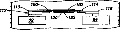
Illustrated among Fig. 4 A-4C wafer 150 has been delivered to robot 64 from robot 62.Described transmission can occur in the position between robot 62 and 64.Shown in Fig. 4 B, the end effector 110 of robot 62 extends wafer 150 on the end effector 114 of robot 64. End effector 110 and 114 is formed and is positioned to make each end effector vertically to move and do not disturb another end effector.In the embodiment of Fig. 4 A, U-shaped end effector 110 can have identical size and dimension with 114, and by lateral shift to allow not limited vertical moving.In this embodiment, wafer 150 is not with respect to one of end effector 110 and 114 or both and be positioned at the center.In another embodiment, end effector 110 and 114 has different shapes and/or yardstick and is positioned at the center to allow wafer 150 with respect to each end effector.For example, the interval between the leg of described U-shaped end effector endways can be different in the actuator 110 and 114, thereby allow two end effectors to be positioned at wafer 150 times and do not disturb.
In operation, the robots arm 112 of robot 62 can be positioned on its middle vertical position, and the robots arm 116 of robot 64 can be positioned on its minimum vertical position.The robots arm 112 of robot 62 extends then so that wafer 150 is positioned on the end effector 114 of robot 64.Shown in Fig. 4 C, the robots arm 116 of robot 64 is increased to its highest vertical position, makes end effector 114 promote wafer 150 from end effector 110.Described then transmission is finished.Robots arm's 112 regractings are carrying out other operation, and robots arm 116 can move to treating stations 68 with wafer 150.
By utilizing the wafer transferring of robot to robot, described object handling system has avoided transmitting the needs at station.Under the situation of utilizing the wafer orientation system, wafer position sensing and correction can need not to transmit the station and carry out.The wafer orientation system that is fit to is below described.
Other basic operation shown in Fig. 5 A-5C comprises by robot 64 wafer 150 being delivered to purpose wafer support 120 and another wafer being removed from box 80.Shown in Fig. 5 B, the robots arm 116 of robot 64 is positioned at its highest vertical position, and wafer 150 is positioned on the purpose wafer support 120.Lifting pin in the purpose wafer support 120 is elevated to the platen (platen) more than the surface that is used to receive wafer 150.Described lifting pin is set on the purpose wafer support 120 to avoid disturbing end effector 114 when robots arm 116 raises and reduces.Robots arm 116 moves to its minimum vertical position then, shown in Fig. 5 C, thus wafer 150 is delivered to the lifting pin of purpose wafer support 120.Robots arm 116 can withdraw from purpose wafer support 120 then, and the lifting pin can be lowered wafer 150 is positioned on the wafer holder surface of purpose wafer support 120 thus.
With wafer 150 is positioned on the purpose wafer support 120 simultaneously, robot 62 can remove second wafer 152 from box 80.Shown in Fig. 5 B, robots arm 112 moves to its minimum vertical position and end effector 110 is located in wafer 152 times.Robots arm 112 is increased to its middle vertical position then, and shown in Fig. 5 C, and wafer 152 is removed from box 80.
The exchange of the wafer shown in Fig. 6 A-6E on the purpose wafer support 120.After handling, robot 62 removes wafer 150 from purpose wafer support 120, and robot 64 is placed on wafer 152 on the purpose wafer support 120 then so that handle.Shown in Fig. 6 B, the robots arm 112 of robot 62 is positioned at its minimum vertical position, and the robots arm 116 of bearing wafer 152 is positioned at its highest vertical position.The lifting pin of purpose wafer support 120 raises, and the clamping surface from purpose wafer support 120 promotes wafer 150 thus.The robots arm 112 of robot 62 extends so that end effector 110 is positioned between the clamping surface of wafer 150 and purpose wafer support 120, and the robots arm 116 of robot 64 extends wafer 152 is positioned at purpose wafer support more than 120, shown in Fig. 6 C.Robots arm 112 withdraws then to remove wafer 150 from purpose wafer support 120.When wafer 150 left purpose wafer support 120, the robots arm 116 of robot 64 was reduced to its minimum vertical position, and wafer 152 is positioned on the lifting pin of purpose wafer support 120, shown in Fig. 6 D.The robots arm 116 of robot 64 withdraws then, and the lifting pin of purpose wafer support 120 reduces thus wafer 152 is positioned on the clamping surface of purpose wafer support 120.The exchange of wafer is finished thus.
Ion inject typically need wafer with respect to the orientation of ion beam with the control channeling effect.Because the position imprecision of the wafer in the box is controlled and owing to can produce unwanted wafer in wafer object handling system when box is delivered to treating stations and move, thereby the wafer orientation system can be used for sensing and calibration wafer site error.Such site error can comprise shift error (degree of eccentricity) and the rotation error with respect to desired location.
The embodiment that is suitable for wafer orientation 130 systems that use in the object handling system of Fig. 2 A is shown in Figure 7.The image of the wafer 150 on the end effector 114 of camera 180 acquisition robots 64.Optionally light source 184 can be as shown from following be that wafer 150 throws light on.In another embodiment, the light source (not shown) can from top be wafer 150 illumination.Be provided for the controller 140 of object handling system from the view data of camera 180.Image analysis software in the controller 140 is analyzed described view data to determine that wafer 150 is with respect to the shift error of the desired location on the end effector 114 and wafer 150 rotation error with respect to required position of rotation.When wafer 150 was placed on the purpose wafer support 120, controller 140 offered control signal in the motor 186 of robot 64 to proofread and correct the shift error of institute's sensing.Particularly, the placement of the wafer 150 on the purpose wafer support 120 is conditioned the shift error with compensation institute sensing.In addition, controller 140 offers motor 188 in the purpose wafer support 120 with control signal.After wafer 150 was positioned on the purpose wafer support 120, purpose wafer support 120 was by the rotation error of motor 188 rotations with compensation institute sensing.The additional detail of relevant wafer orientation system is disclosed in the above-mentioned United States Patent (USP) 6,144,705 that is hereby incorporated by.As an alternative, can when being located in the robot 62, wafer 150 obtain the image of wafer 150.Yet, will not consider that in the trimming process of position robot is during the robotic delivery and any slip of wafer 150 afterwards.
The wafer orientation system is not limited to the image sensing to the wafer position error.Include but not limited to RF electric field sensing, magnetic resonance sensing, laser scanning and utilize the detection technology of photodetector array sensing for example can be used to location sensing.In addition, some treatment system tolerable wafer position errors, and can not need to use the wafer orientation system.In addition, the system that is used to dispose the workpiece except that semiconductor wafer may need or may not need accurate workpiece location and may need thus or may not need workpiece positioning system.
The flow chart of process instance that is used for the wafer of process cartridge 80 and 82 shown in Fig. 8 A and the 8B.Described process can be controlled by the software in the controller 140.Described process comprises shown in Fig. 2 A-2C, 3,4A-4C, 5A-5C, the 6A-6E and 7 and above-described basic operation.In step 200, first wafer is delivered to treating stations 68 from box 80.The transmission of first wafer in step 200 comprises: (1) removes wafer from box 80, shown in Fig. 2 A-2C and 3 and the above, (2) from robot 62 to robot 64 robot to robotic delivery, shown in Fig. 4 A-4C and the above, (3) wafer position sensing and correction, as described above in connection with Figure 7, and (4) by robot 64 with wafer transferring to purpose wafer support 120, as above in conjunction with as described in Fig. 5 A-5C.
When described first wafer being loaded into treating stations 68, described process advances to step 202.In step 202, robot 62 removes wafer n (wherein n is wafer number or index) from box 80, shown in Fig. 2 A-2C and 3 and the above.In step 204, robot 62 is delivered to robot 64 with wafer n, shown in Fig. 4 A-4C and the above.Also in step 204, shift error and the rotation error of the 130 sensing wafer n of wafer orientation system, as described above in connection with Figure 7.In step 206, robot 62 removes wafer n-1 from purpose wafer support 120, as above in conjunction with as described in Fig. 6 A-6C.In step 208, robot 64 is placed on wafer n on the purpose wafer support 120, and in conjunction with as described in Fig. 6 A, 6D and the 6E, and described placement is conditioned the shift error with institute's sensing of calibration wafer n as above, as described above in connection with Figure 7.In step 210, purpose wafer support 120 rotations are with the rotation error of institute's sensing of calibration wafer n, as described above in connection with Figure 7.In step 212, robot 62 turns back to box 80 with wafer n-1, as above in conjunction with as described in Fig. 2 A-2C.In step 216, determine whether that wafer n is the final wafer (n=n in the box
Max).If wafer n is not last wafer, then by increment, and 84 pairs of boxes of lifter 80 carry out index so that visit next wafer to wafer index n in step 218.Any step 202 that turns back to of described process is to remove described next wafer from box 80.Next wafer is handled in an identical manner.If determine that in step 216 wafer n (current on purpose wafer support) is last wafer, then wafer n is unloaded from treating stations 68 and is turned back to box 80 in step 220, as described in above integrating step 206 and 212.
When completing steps 220, all wafers in the box 80 is treated and turn back to box 80.In step 230, robot 62 and 64 role are switched to allow the wafer in the handle box 82 in the object handling process.In step 232, the process of coming repeating step 200-220 at box 82, and box 80 can be changed into the new box that comprises untreated wafer.Described process turns back to its box of therefrom removing and continues to handle other box and wafer thus.
Workpiece disposal system described herein is advantageously used in disposes semiconductor wafer and other disk type work.Yet the present invention is not limited to this respect and can be used for disposing the workpiece of other type, and the suitable remodeling to the system element of support and travelling workpiece is wherein arranged.
After aspect having described at least one embodiment of the present invention several thus, should understand those skilled in the art and can expect various changes, remodeling and improvement easily.Such change, remodeling and improvement are intended for part of the present disclosure, and are intended to be in the spirit and scope of the present invention.Therefore, above specification and accompanying drawing only are as an example.
Claims (26)
1. one kind is used for the method that workpiece is disposed, and comprising:
(a) utilize first robot to remove workpiece from first box;
(b) described workpiece is directly delivered to second robot and described workpiece is not delivered to the transmission station from described first robot;
(c) utilize described second robot described workpiece to be placed on the workpiece supporter at treating stations place; And
(d) after handling, utilize described first robot that described workpiece is delivered to described first box from described workpiece supporter.
2. method as claimed in claim 1 comprises further that the described workpiece of sensing need not to use with respect to the described shift error of the shift error of fiducial value and rotation error and calibration of workpieces and rotation error to transmit the station.
3. method as claimed in claim 2 is wherein proofreaied and correct shift error and rotation error and is comprised and utilize described second robot to proofread and correct shift error and utilize described workpiece supporter to proofread and correct rotation error.
4. method as claimed in claim 2, wherein sensing shift error and rotation error comprise:
The image that obtains workpiece is to provide view data and to handle described view data to determine shift error and the rotation error with respect to described fiducial value.
5. method as claimed in claim 2, wherein sensing shift error and rotation error comprise:
Obtain the measured value of workpiece and handle described measured value to determine shift error and rotation error with respect to described fiducial value.
6. method as claimed in claim 5 wherein obtains measured value and uses from by selected detection technology the following group of forming: RF electric field sensing, magnetic resonance sensing, laser scanning and utilize the photodetector array sensing.
7. method as claimed in claim 1, wherein said first and second robots each comprise can be laterally and the vertical end effector that moves.
8. method as claimed in claim 7, each has a plurality of discrete vertical positions the end effector of wherein said first and second robots.
9. method as claimed in claim 1, wherein, described second robot comprises end effector, and step (b) comprises that described first robot is positioned described workpiece on the end effector of described second robot and described second robot promotes described workpiece from described first robot.
10. method as claimed in claim 1, wherein, described first robot comprises end effector, and step (a) comprises that the end effector with described first robot extends in described first box below described workpiece, the end effector of described first robot and the end effector of described first robot that withdraws from described first box raise.
11. method as claimed in claim 1, wherein, described first robot comprises that end effector and described second robot comprise end effector, and wherein step (b) comprises that the end effector of described first robot and end effector that described second robot is located by described second robot are located by described first robot so that avoid interference between the end effector of the end effector of described first robot and described second robot when mobile when at least one of the end effector of the end effector of described first robot and described second robot is vertical.
12. method as claimed in claim 1, wherein step (a)-(d) is suitable for disposing semiconductor wafer.
13. one kind is used for the method that workpiece is disposed, comprises:
(a) utilize first robot to remove first workpiece from first box;
(b) described first workpiece is directly delivered to second robot and described first workpiece is not delivered to the transmission station from described first robot;
(c) utilize described second robot described first workpiece to be placed on the workpiece supporter at treating stations place;
(d) utilize described first robot to remove second workpiece from described first box;
(e) described second workpiece is directly delivered to described second robot and described second workpiece is not delivered to the transmission station from described first robot;
(f) utilize described first robot that described first workpiece is delivered to described first box from described workpiece supporter;
(g) utilize described second robot described second workpiece to be placed on the described workpiece supporter at described treating stations place; And
(h) at all the other the workpiece repeating steps (d)-(g) in described first box.
14. the method as claim 13 further comprises:
Switch the role of described first robot and second robot and at the workpiece repeating step (a)-(h) in second box.
15. as the method for claim 13, wherein step (g) is included in before first workpiece removed from described workpiece supporter by described first robot, described second robot is positioned at second workpiece more than the described workpiece supporter.
16. method as claim 15, wherein, described first robot comprises that end effector and described second robot comprise end effector, and wherein second workpiece is positioned at and comprises more than the described workpiece supporter that described first robot is positioned at first vertical position with the end effector of described first robot and the end effector of described first robot is extended below described first workpiece, and the end effector that described second robot is positioned at second vertical position with the end effector of described second robot and will carries described second robot of described second workpiece extends on the described workpiece supporter.
17. a workpiece disposal system comprises:
Vacuum chamber;
Treating stations is in described vacuum chamber;
First and second vacuum locks controllably are coupled in described vacuum chamber by first and second isolating valves respectively; And
First and second robots, in described vacuum chamber, be used for workpiece is delivered between described vacuum lock and the described treating stations, each has the robots arm described first and second robots, this robots arm can vertically move to varying level, and can laterally move to allow that the direct robot of workpiece is arrived robotic delivery, transmit the station and workpiece is not delivered to.
18., further comprise being used to control the described first and second ROBOT CONTROL devices as the workpiece disposal system of claim 17.
19. as the workpiece disposal system of claim 18, wherein said controller control comprises following operation: utilize described first robot to remove workpiece from first box; Described workpiece is directly delivered to described second robot from described first robot; Utilize described second robot described workpiece to be placed on the workpiece supporter at described treating stations place; And after handling, utilize described first robot that described workpiece is delivered to described first box from described workpiece supporter.
20. as the workpiece disposal system of claim 19, wherein said controller further control comprises following operation: dispose the workpiece in described first box.
21. as the workpiece disposal system of claim 20, wherein said controller further control comprises following operation: switch the role of described first robot and described second robot, and dispose the workpiece in second box.
22. as the workpiece disposal system of claim 19, wherein the operation that described workpiece is placed on the workpiece supporter comprises: before described workpiece supporter is removed, second workpiece is positioned at more than the described workpiece supporter at first workpiece.
23. workpiece disposal system as claim 19, further comprise workpiece positioning system, be used for shift error and the rotation error of the described workpiece of sensing, and be used to proofread and correct the described shift error of described workpiece and rotation error and need not to use and transmit the station with respect to fiducial value.
24. as the workpiece disposal system of claim 23, wherein said workpiece positioning system comprises and is used to utilize described second robot to proofread and correct the device of shift error and is used to utilize described workpiece supporter to proofread and correct the device of rotation error.
25. workpiece disposal system as claim 23, wherein said workpiece positioning system comprises camera and image analysis software, the image that described camera is used to obtain workpiece is to provide view data, and described image analysis software is used to handle described view data to determine shift error and the rotation error with respect to described fiducial value.
26. as the workpiece disposal system of claim 17, wherein said first and second robots are configured for the disposal semiconductor wafer.
Applications Claiming Priority (2)
| Application Number | Priority Date | Filing Date | Title |
|---|---|---|---|
| US10/395,940 US6748293B1 (en) | 2003-03-24 | 2003-03-24 | Methods and apparatus for high speed object handling |
| US10/395,940 | 2003-03-24 |
Publications (2)
| Publication Number | Publication Date |
|---|---|
| CN1765004A CN1765004A (en) | 2006-04-26 |
| CN100385614C true CN100385614C (en) | 2008-04-30 |
Family
ID=32326203
Family Applications (1)
| Application Number | Title | Priority Date | Filing Date |
|---|---|---|---|
| CNB2004800080710A Expired - Fee Related CN100385614C (en) | 2003-03-24 | 2004-03-24 | Methods and apparatus for high speed object handling |
Country Status (5)
| Country | Link |
|---|---|
| US (1) | US6748293B1 (en) |
| JP (1) | JP4727572B2 (en) |
| KR (1) | KR100969058B1 (en) |
| CN (1) | CN100385614C (en) |
| WO (1) | WO2004086465A2 (en) |
Families Citing this family (40)
| Publication number | Priority date | Publication date | Assignee | Title |
|---|---|---|---|---|
| JP4696373B2 (en) * | 2001-02-20 | 2011-06-08 | 東京エレクトロン株式会社 | Processing system and method of conveying object |
| US6852194B2 (en) * | 2001-05-21 | 2005-02-08 | Tokyo Electron Limited | Processing apparatus, transferring apparatus and transferring method |
| DE60214763T2 (en) * | 2001-11-29 | 2007-09-06 | Diamond Semiconductor Group LLC., Gloucester | WAFER HANDLING DEVICE AND METHOD THEREFOR |
| JP3865703B2 (en) * | 2002-10-25 | 2007-01-10 | ファナック株式会社 | Article conveying system and conveying method |
| KR100577582B1 (en) * | 2004-06-09 | 2006-05-08 | 삼성전자주식회사 | Spinner for manufacturing semiconductor device and method for preventing wafer teaching badness at the same |
| US8668422B2 (en) * | 2004-08-17 | 2014-03-11 | Mattson Technology, Inc. | Low cost high throughput processing platform |
| JP4907077B2 (en) * | 2004-11-30 | 2012-03-28 | 株式会社Sen | Wafer processing apparatus, wafer processing method, and ion implantation apparatus |
| US7585141B2 (en) * | 2005-02-01 | 2009-09-08 | Varian Semiconductor Equipment Associates, Inc. | Load lock system for ion beam processing |
| US8118535B2 (en) * | 2005-05-18 | 2012-02-21 | International Business Machines Corporation | Pod swapping internal to tool run time |
| JP2007005582A (en) * | 2005-06-24 | 2007-01-11 | Asm Japan Kk | Substrate transfer apparatus and semiconductor substrate manufacturing apparatus mounted with the same |
| JP4440178B2 (en) * | 2005-07-25 | 2010-03-24 | 東京エレクトロン株式会社 | Substrate transfer device |
| US7690881B2 (en) * | 2006-08-30 | 2010-04-06 | Asm Japan K.K. | Substrate-processing apparatus with buffer mechanism and substrate-transferring apparatus |
| US7740437B2 (en) | 2006-09-22 | 2010-06-22 | Asm International N.V. | Processing system with increased cassette storage capacity |
| US20080075563A1 (en) * | 2006-09-27 | 2008-03-27 | Mclane James R | Substrate handling system and method |
| US7585142B2 (en) * | 2007-03-16 | 2009-09-08 | Asm America, Inc. | Substrate handling chamber with movable substrate carrier loading platform |
| US7953511B1 (en) * | 2007-09-21 | 2011-05-31 | National Semiconductor Corporation | System and method for reducing processing errors during wafer fabrication employing a 2D wafer scribe and monitoring system |
| JP5336513B2 (en) | 2007-12-27 | 2013-11-06 | ラム リサーチ コーポレーション | System and method for dynamic alignment beam calibration |
| JP5309157B2 (en) | 2007-12-27 | 2013-10-09 | ラム リサーチ コーポレーション | System and method for calibrating end effector alignment in a plasma processing system |
| WO2009086164A2 (en) * | 2007-12-27 | 2009-07-09 | Lam Research Corporation | Systems and methods for calibrating end effector alignment using at least a light source |
| SG195592A1 (en) | 2007-12-27 | 2013-12-30 | Lam Res Corp | Arrangements and methods for determining positions and offsets in plasma processing system |
| FR2931295B1 (en) * | 2008-05-13 | 2010-08-20 | Altatech Semiconductor | DEVICE AND METHOD FOR INSPECTING SEMICONDUCTOR WAFERS |
| US9254566B2 (en) * | 2009-03-13 | 2016-02-09 | Kawasaki Jukogyo Kabushiki Kaisha | Robot having end effector and method of operating the same |
| US8970820B2 (en) | 2009-05-20 | 2015-03-03 | Nikon Corporation | Object exchange method, exposure method, carrier system, exposure apparatus, and device manufacturing method |
| US8285418B2 (en) * | 2009-07-23 | 2012-10-09 | Kla-Tencor Corporation | Dual scanning stage |
| JP5477133B2 (en) * | 2010-04-09 | 2014-04-23 | 日新イオン機器株式会社 | Wafer handling method and ion implantation apparatus |
| CN102310999B (en) * | 2010-07-09 | 2013-07-17 | 上海凯世通半导体有限公司 | Vacuum transmission process equipment and method |
| JP2012243335A (en) * | 2011-05-17 | 2012-12-10 | Sony Corp | Disk conveyance device and disk storage system |
| JP5573861B2 (en) * | 2012-02-16 | 2014-08-20 | 株式会社安川電機 | Transport system |
| KR102074534B1 (en) * | 2012-06-06 | 2020-03-02 | 에베 그룹 에. 탈너 게엠베하 | Apparatus and method for ascertaining orientation errors |
| JP2013110114A (en) * | 2012-12-27 | 2013-06-06 | Hitachi High-Technologies Corp | Apparatus for manufacturing organic el device and angle correction mechanism |
| US10224232B2 (en) | 2013-01-18 | 2019-03-05 | Persimmon Technologies Corporation | Robot having two arms with unequal link lengths |
| US9149936B2 (en) | 2013-01-18 | 2015-10-06 | Persimmon Technologies, Corp. | Robot having arm with unequal link lengths |
| JP6235612B2 (en) * | 2013-01-18 | 2017-11-22 | パーシモン テクノロジーズ コーポレイションPersimmon Technologies, Corp. | Robot with arm having unequal link length |
| WO2016122897A1 (en) * | 2015-01-28 | 2016-08-04 | Kla-Tencor Corporation | Flipping apparatus, system and method for processing articles |
| US9783372B2 (en) | 2015-01-28 | 2017-10-10 | Kla-Tencor Corporation | Flipping apparatus, system and method for processing articles |
| KR102567510B1 (en) | 2015-03-12 | 2023-08-17 | 퍼시몬 테크놀로지스 코포레이션 | Robots with subordinated end effector movements |
| US9831110B2 (en) | 2015-07-30 | 2017-11-28 | Lam Research Corporation | Vision-based wafer notch position measurement |
| US10724967B2 (en) | 2018-04-20 | 2020-07-28 | Samsung Electronics Co., Ltd. | Inspection apparatus for semiconductor process and semiconductor process device |
| US11626305B2 (en) * | 2019-06-25 | 2023-04-11 | Applied Materials, Inc. | Sensor-based correction of robot-held object |
| US11335578B2 (en) * | 2020-02-13 | 2022-05-17 | Kawasaki Jukogyo Kabushiki Kaisha | Substrate transfer apparatus and method of measuring positional deviation of substrate |
Citations (6)
| Publication number | Priority date | Publication date | Assignee | Title |
|---|---|---|---|---|
| US5486080A (en) * | 1994-06-30 | 1996-01-23 | Diamond Semiconductor Group, Inc. | High speed movement of workpieces in vacuum processing |
| US6007675A (en) * | 1996-07-09 | 1999-12-28 | Gamma Precision Technology, Inc. | Wafer transfer system and method of using the same |
| US6045315A (en) * | 1997-08-25 | 2000-04-04 | Shibaura Engineering Works Co., Ltd. | Robot apparatus and treating apparatus |
| US6114705A (en) * | 1997-09-10 | 2000-09-05 | Varian Semiconductor Equipment Associates, Inc. | System for correcting eccentricity and rotational error of a workpiece |
| WO2001010756A1 (en) * | 1999-08-11 | 2001-02-15 | Multilevel Metals, Inc. | Load lock system for foups |
| US6315512B1 (en) * | 1997-11-28 | 2001-11-13 | Mattson Technology, Inc. | Systems and methods for robotic transfer of workpieces between a storage area and a processing chamber |
Family Cites Families (27)
| Publication number | Priority date | Publication date | Assignee | Title |
|---|---|---|---|---|
| US3901183A (en) | 1973-06-12 | 1975-08-26 | Extrion Corp | Wafer treatment apparatus |
| US4008683A (en) | 1973-07-16 | 1977-02-22 | Varian Associates | Machine for treating wafer-form items |
| US4282924A (en) | 1979-03-16 | 1981-08-11 | Varian Associates, Inc. | Apparatus for mechanically clamping semiconductor wafer against pliable thermally conductive surface |
| DE3219502C2 (en) | 1982-05-25 | 1990-04-19 | Ernst Leitz Wetzlar Gmbh, 6330 Wetzlar | Device for the automatic transport of disc-shaped objects |
| US4836733A (en) | 1986-04-28 | 1989-06-06 | Varian Associates, Inc. | Wafer transfer system |
| JPS6464231A (en) | 1987-09-03 | 1989-03-10 | Toshiba Corp | Conveyor |
| JPH0825151B2 (en) | 1988-09-16 | 1996-03-13 | 東京応化工業株式会社 | Handling unit |
| WO1991004213A1 (en) | 1989-09-12 | 1991-04-04 | Rapro Technology, Inc. | Automated wafer transport system |
| US5186594A (en) | 1990-04-19 | 1993-02-16 | Applied Materials, Inc. | Dual cassette load lock |
| US5286296A (en) | 1991-01-10 | 1994-02-15 | Sony Corporation | Multi-chamber wafer process equipment having plural, physically communicating transfer means |
| JPH05275511A (en) * | 1991-03-01 | 1993-10-22 | Tokyo Electron Ltd | Transferring system and treating device for object to be treated |
| JPH04295704A (en) * | 1991-03-25 | 1992-10-20 | Kokusai Electric Co Ltd | Apparatus for detecting central position of wafer |
| JPH0785469B2 (en) * | 1991-09-05 | 1995-09-13 | 日新ハイボルテージ株式会社 | Wafer transfer device in ion implantation system |
| US5404894A (en) | 1992-05-20 | 1995-04-11 | Tokyo Electron Kabushiki Kaisha | Conveyor apparatus |
| JP3320539B2 (en) * | 1993-12-17 | 2002-09-03 | 東京エレクトロン株式会社 | Equipment for loading and unloading objects |
| JPH07263518A (en) * | 1994-03-18 | 1995-10-13 | Fujitsu Ltd | Method and apparatus for transferring semiconductor wafer, and wafer treatment method |
| JPH09102530A (en) | 1995-06-07 | 1997-04-15 | Varian Assoc Inc | Direction inspection system of wafer |
| US6481956B1 (en) * | 1995-10-27 | 2002-11-19 | Brooks Automation Inc. | Method of transferring substrates with two different substrate holding end effectors |
| US6491491B1 (en) * | 1997-10-30 | 2002-12-10 | Sankyo Seiki Mfg. Co., Ltd. | Articulated robot |
| JP3778677B2 (en) * | 1997-12-01 | 2006-05-24 | 大日本スクリーン製造株式会社 | Substrate processing equipment |
| JPH11260889A (en) * | 1998-03-13 | 1999-09-24 | Ebara Corp | Ion implanting apparatus |
| US6323616B1 (en) * | 1999-03-15 | 2001-11-27 | Berkeley Process Control, Inc. | Self teaching robotic wafer handling system |
| TW494523B (en) * | 2000-04-05 | 2002-07-11 | Tokyo Electron Ltd | Processing device |
| JP2002026104A (en) * | 2000-06-30 | 2002-01-25 | Dainippon Printing Co Ltd | Delivering apparatus and delivering method by robot |
| JP2002270672A (en) * | 2001-03-09 | 2002-09-20 | Olympus Optical Co Ltd | Method of alignment and substrate-inspecting apparatus |
| JP4435443B2 (en) * | 2001-04-17 | 2010-03-17 | 大日本スクリーン製造株式会社 | Substrate transport apparatus and substrate transport method |
| JP2002313874A (en) * | 2001-04-17 | 2002-10-25 | Dainippon Screen Mfg Co Ltd | Substrate support member, substrate retention mechanism using the same, substrate conveyance apparatus and method therefor, and substrate treatment apparatus and method therefor |
-
2003
- 2003-03-24 US US10/395,940 patent/US6748293B1/en not_active Expired - Fee Related
-
2004
- 2004-03-24 JP JP2006507513A patent/JP4727572B2/en not_active Expired - Fee Related
- 2004-03-24 KR KR1020057017796A patent/KR100969058B1/en active IP Right Grant
- 2004-03-24 WO PCT/US2004/008942 patent/WO2004086465A2/en active Application Filing
- 2004-03-24 CN CNB2004800080710A patent/CN100385614C/en not_active Expired - Fee Related
Patent Citations (6)
| Publication number | Priority date | Publication date | Assignee | Title |
|---|---|---|---|---|
| US5486080A (en) * | 1994-06-30 | 1996-01-23 | Diamond Semiconductor Group, Inc. | High speed movement of workpieces in vacuum processing |
| US6007675A (en) * | 1996-07-09 | 1999-12-28 | Gamma Precision Technology, Inc. | Wafer transfer system and method of using the same |
| US6045315A (en) * | 1997-08-25 | 2000-04-04 | Shibaura Engineering Works Co., Ltd. | Robot apparatus and treating apparatus |
| US6114705A (en) * | 1997-09-10 | 2000-09-05 | Varian Semiconductor Equipment Associates, Inc. | System for correcting eccentricity and rotational error of a workpiece |
| US6315512B1 (en) * | 1997-11-28 | 2001-11-13 | Mattson Technology, Inc. | Systems and methods for robotic transfer of workpieces between a storage area and a processing chamber |
| WO2001010756A1 (en) * | 1999-08-11 | 2001-02-15 | Multilevel Metals, Inc. | Load lock system for foups |
Also Published As
| Publication number | Publication date |
|---|---|
| WO2004086465A3 (en) | 2004-11-25 |
| KR20050118682A (en) | 2005-12-19 |
| CN1765004A (en) | 2006-04-26 |
| WO2004086465A2 (en) | 2004-10-07 |
| JP4727572B2 (en) | 2011-07-20 |
| KR100969058B1 (en) | 2010-07-09 |
| US6748293B1 (en) | 2004-06-08 |
| JP2006521704A (en) | 2006-09-21 |
Similar Documents
| Publication | Publication Date | Title |
|---|---|---|
| CN100385614C (en) | Methods and apparatus for high speed object handling | |
| CN108028218B (en) | Substrate transfer robot and substrate processing system | |
| KR101015778B1 (en) | Substrate processing apparatus and method for adjusting a substrate transfer position | |
| JP2006521704A5 (en) | ||
| US6729462B2 (en) | Edge grip aligner with buffering capabilities | |
| US6032083A (en) | Substrate transfer apparatus and heat treatment system using the same | |
| CN107534007B (en) | Substrate transfer robot and substrate processing system | |
| CN101548374A (en) | High throughput wafer notch aligner | |
| JP2005019963A (en) | Substrate processor and method of adjusting substrate delivery position | |
| JP2003506879A (en) | Rectangular wafer alignment system | |
| US6478532B1 (en) | Wafer orienting and reading mechanism | |
| KR101013019B1 (en) | Wafer transfer system and transfer method | |
| US6114705A (en) | System for correcting eccentricity and rotational error of a workpiece | |
| EP1357589A4 (en) | Workpiece transfer system, transfer method, vacuum chuck, and wafer centering method | |
| EP2346073B1 (en) | Prealigner | |
| JP2005011966A (en) | Substrate transporting device, substrate processing device, conveyance reference position teaching method and sensor jig used for them | |
| JP4501102B2 (en) | Teaching jig, robot taught using the same and teaching method of the robot | |
| US20020150456A1 (en) | Method and apparatus for transferring a wafer | |
| JP3625013B2 (en) | Substrate transport apparatus positioning method and apparatus | |
| US20220181178A1 (en) | Correction method and substrate transfer apparatus | |
| KR200238689Y1 (en) | Load Lock Chamber of Scanning Electron Microscope | |
| KR20220114775A (en) | Wafer transfer device and method of transferring wafer using the same | |
| CN117253835A (en) | Graphite disc positioning mechanism for loading wafer | |
| KR20000014177A (en) | Wafer transfer equipment | |
| KR20040009242A (en) | Wafer conduction equipment having the aligner and the methode there of |
Legal Events
| Date | Code | Title | Description |
|---|---|---|---|
| C06 | Publication | ||
| PB01 | Publication | ||
| C10 | Entry into substantive examination | ||
| SE01 | Entry into force of request for substantive examination | ||
| C14 | Grant of patent or utility model | ||
| GR01 | Patent grant | ||
| CF01 | Termination of patent right due to non-payment of annual fee | ||
| CF01 | Termination of patent right due to non-payment of annual fee |
Granted publication date: 20080430 Termination date: 20160324 |