CN100367451C - 半导体装置及其制造方法 - Google Patents
半导体装置及其制造方法 Download PDFInfo
- Publication number
- CN100367451C CN100367451C CNB2004100562611A CN200410056261A CN100367451C CN 100367451 C CN100367451 C CN 100367451C CN B2004100562611 A CNB2004100562611 A CN B2004100562611A CN 200410056261 A CN200410056261 A CN 200410056261A CN 100367451 C CN100367451 C CN 100367451C
- Authority
- CN
- China
- Prior art keywords
- distribution
- semiconductor
- dielectric film
- semiconductor device
- semiconductor substrate
- Prior art date
- Legal status (The legal status is an assumption and is not a legal conclusion. Google has not performed a legal analysis and makes no representation as to the accuracy of the status listed.)
- Expired - Fee Related
Links
Images


Classifications
-
- H—ELECTRICITY
- H01—ELECTRIC ELEMENTS
- H01L—SEMICONDUCTOR DEVICES NOT COVERED BY CLASS H10
- H01L24/00—Arrangements for connecting or disconnecting semiconductor or solid-state bodies; Methods or apparatus related thereto
- H01L24/01—Means for bonding being attached to, or being formed on, the surface to be connected, e.g. chip-to-package, die-attach, "first-level" interconnects; Manufacturing methods related thereto
- H01L24/10—Bump connectors ; Manufacturing methods related thereto
- H01L24/12—Structure, shape, material or disposition of the bump connectors prior to the connecting process
- H01L24/13—Structure, shape, material or disposition of the bump connectors prior to the connecting process of an individual bump connector
-
- H—ELECTRICITY
- H01—ELECTRIC ELEMENTS
- H01L—SEMICONDUCTOR DEVICES NOT COVERED BY CLASS H10
- H01L23/00—Details of semiconductor or other solid state devices
- H01L23/12—Mountings, e.g. non-detachable insulating substrates
-
- H—ELECTRICITY
- H01—ELECTRIC ELEMENTS
- H01L—SEMICONDUCTOR DEVICES NOT COVERED BY CLASS H10
- H01L21/00—Processes or apparatus adapted for the manufacture or treatment of semiconductor or solid state devices or of parts thereof
- H01L21/67—Apparatus specially adapted for handling semiconductor or electric solid state devices during manufacture or treatment thereof; Apparatus specially adapted for handling wafers during manufacture or treatment of semiconductor or electric solid state devices or components ; Apparatus not specifically provided for elsewhere
- H01L21/683—Apparatus specially adapted for handling semiconductor or electric solid state devices during manufacture or treatment thereof; Apparatus specially adapted for handling wafers during manufacture or treatment of semiconductor or electric solid state devices or components ; Apparatus not specifically provided for elsewhere for supporting or gripping
- H01L21/6835—Apparatus specially adapted for handling semiconductor or electric solid state devices during manufacture or treatment thereof; Apparatus specially adapted for handling wafers during manufacture or treatment of semiconductor or electric solid state devices or components ; Apparatus not specifically provided for elsewhere for supporting or gripping using temporarily an auxiliary support
- H01L21/6836—Wafer tapes, e.g. grinding or dicing support tapes
-
- H—ELECTRICITY
- H01—ELECTRIC ELEMENTS
- H01L—SEMICONDUCTOR DEVICES NOT COVERED BY CLASS H10
- H01L21/00—Processes or apparatus adapted for the manufacture or treatment of semiconductor or solid state devices or of parts thereof
- H01L21/70—Manufacture or treatment of devices consisting of a plurality of solid state components formed in or on a common substrate or of parts thereof; Manufacture of integrated circuit devices or of parts thereof
- H01L21/77—Manufacture or treatment of devices consisting of a plurality of solid state components or integrated circuits formed in, or on, a common substrate
- H01L21/78—Manufacture or treatment of devices consisting of a plurality of solid state components or integrated circuits formed in, or on, a common substrate with subsequent division of the substrate into plural individual devices
-
- H—ELECTRICITY
- H01—ELECTRIC ELEMENTS
- H01L—SEMICONDUCTOR DEVICES NOT COVERED BY CLASS H10
- H01L23/00—Details of semiconductor or other solid state devices
- H01L23/28—Encapsulations, e.g. encapsulating layers, coatings, e.g. for protection
- H01L23/31—Encapsulations, e.g. encapsulating layers, coatings, e.g. for protection characterised by the arrangement or shape
- H01L23/3107—Encapsulations, e.g. encapsulating layers, coatings, e.g. for protection characterised by the arrangement or shape the device being completely enclosed
- H01L23/3114—Encapsulations, e.g. encapsulating layers, coatings, e.g. for protection characterised by the arrangement or shape the device being completely enclosed the device being a chip scale package, e.g. CSP
-
- H—ELECTRICITY
- H01—ELECTRIC ELEMENTS
- H01L—SEMICONDUCTOR DEVICES NOT COVERED BY CLASS H10
- H01L24/00—Arrangements for connecting or disconnecting semiconductor or solid-state bodies; Methods or apparatus related thereto
- H01L24/01—Means for bonding being attached to, or being formed on, the surface to be connected, e.g. chip-to-package, die-attach, "first-level" interconnects; Manufacturing methods related thereto
- H01L24/10—Bump connectors ; Manufacturing methods related thereto
- H01L24/11—Manufacturing methods
-
- H—ELECTRICITY
- H01—ELECTRIC ELEMENTS
- H01L—SEMICONDUCTOR DEVICES NOT COVERED BY CLASS H10
- H01L2221/00—Processes or apparatus adapted for the manufacture or treatment of semiconductor or solid state devices or of parts thereof covered by H01L21/00
- H01L2221/67—Apparatus for handling semiconductor or electric solid state devices during manufacture or treatment thereof; Apparatus for handling wafers during manufacture or treatment of semiconductor or electric solid state devices or components; Apparatus not specifically provided for elsewhere
- H01L2221/683—Apparatus for handling semiconductor or electric solid state devices during manufacture or treatment thereof; Apparatus for handling wafers during manufacture or treatment of semiconductor or electric solid state devices or components; Apparatus not specifically provided for elsewhere for supporting or gripping
- H01L2221/68304—Apparatus for handling semiconductor or electric solid state devices during manufacture or treatment thereof; Apparatus for handling wafers during manufacture or treatment of semiconductor or electric solid state devices or components; Apparatus not specifically provided for elsewhere for supporting or gripping using temporarily an auxiliary support
- H01L2221/68327—Apparatus for handling semiconductor or electric solid state devices during manufacture or treatment thereof; Apparatus for handling wafers during manufacture or treatment of semiconductor or electric solid state devices or components; Apparatus not specifically provided for elsewhere for supporting or gripping using temporarily an auxiliary support used during dicing or grinding
-
- H—ELECTRICITY
- H01—ELECTRIC ELEMENTS
- H01L—SEMICONDUCTOR DEVICES NOT COVERED BY CLASS H10
- H01L2221/00—Processes or apparatus adapted for the manufacture or treatment of semiconductor or solid state devices or of parts thereof covered by H01L21/00
- H01L2221/67—Apparatus for handling semiconductor or electric solid state devices during manufacture or treatment thereof; Apparatus for handling wafers during manufacture or treatment of semiconductor or electric solid state devices or components; Apparatus not specifically provided for elsewhere
- H01L2221/683—Apparatus for handling semiconductor or electric solid state devices during manufacture or treatment thereof; Apparatus for handling wafers during manufacture or treatment of semiconductor or electric solid state devices or components; Apparatus not specifically provided for elsewhere for supporting or gripping
- H01L2221/68304—Apparatus for handling semiconductor or electric solid state devices during manufacture or treatment thereof; Apparatus for handling wafers during manufacture or treatment of semiconductor or electric solid state devices or components; Apparatus not specifically provided for elsewhere for supporting or gripping using temporarily an auxiliary support
- H01L2221/68372—Apparatus for handling semiconductor or electric solid state devices during manufacture or treatment thereof; Apparatus for handling wafers during manufacture or treatment of semiconductor or electric solid state devices or components; Apparatus not specifically provided for elsewhere for supporting or gripping using temporarily an auxiliary support used to support a device or wafer when forming electrical connections thereto
-
- H—ELECTRICITY
- H01—ELECTRIC ELEMENTS
- H01L—SEMICONDUCTOR DEVICES NOT COVERED BY CLASS H10
- H01L2224/00—Indexing scheme for arrangements for connecting or disconnecting semiconductor or solid-state bodies and methods related thereto as covered by H01L24/00
- H01L2224/01—Means for bonding being attached to, or being formed on, the surface to be connected, e.g. chip-to-package, die-attach, "first-level" interconnects; Manufacturing methods related thereto
- H01L2224/02—Bonding areas; Manufacturing methods related thereto
- H01L2224/023—Redistribution layers [RDL] for bonding areas
- H01L2224/0231—Manufacturing methods of the redistribution layers
- H01L2224/02313—Subtractive methods
-
- H—ELECTRICITY
- H01—ELECTRIC ELEMENTS
- H01L—SEMICONDUCTOR DEVICES NOT COVERED BY CLASS H10
- H01L2224/00—Indexing scheme for arrangements for connecting or disconnecting semiconductor or solid-state bodies and methods related thereto as covered by H01L24/00
- H01L2224/01—Means for bonding being attached to, or being formed on, the surface to be connected, e.g. chip-to-package, die-attach, "first-level" interconnects; Manufacturing methods related thereto
- H01L2224/02—Bonding areas; Manufacturing methods related thereto
- H01L2224/04—Structure, shape, material or disposition of the bonding areas prior to the connecting process
- H01L2224/0401—Bonding areas specifically adapted for bump connectors, e.g. under bump metallisation [UBM]
-
- H—ELECTRICITY
- H01—ELECTRIC ELEMENTS
- H01L—SEMICONDUCTOR DEVICES NOT COVERED BY CLASS H10
- H01L2224/00—Indexing scheme for arrangements for connecting or disconnecting semiconductor or solid-state bodies and methods related thereto as covered by H01L24/00
- H01L2224/01—Means for bonding being attached to, or being formed on, the surface to be connected, e.g. chip-to-package, die-attach, "first-level" interconnects; Manufacturing methods related thereto
- H01L2224/02—Bonding areas; Manufacturing methods related thereto
- H01L2224/04—Structure, shape, material or disposition of the bonding areas prior to the connecting process
- H01L2224/05—Structure, shape, material or disposition of the bonding areas prior to the connecting process of an individual bonding area
- H01L2224/0554—External layer
- H01L2224/05575—Plural external layers
- H01L2224/0558—Plural external layers being stacked
-
- H—ELECTRICITY
- H01—ELECTRIC ELEMENTS
- H01L—SEMICONDUCTOR DEVICES NOT COVERED BY CLASS H10
- H01L2224/00—Indexing scheme for arrangements for connecting or disconnecting semiconductor or solid-state bodies and methods related thereto as covered by H01L24/00
- H01L2224/01—Means for bonding being attached to, or being formed on, the surface to be connected, e.g. chip-to-package, die-attach, "first-level" interconnects; Manufacturing methods related thereto
- H01L2224/02—Bonding areas; Manufacturing methods related thereto
- H01L2224/04—Structure, shape, material or disposition of the bonding areas prior to the connecting process
- H01L2224/05—Structure, shape, material or disposition of the bonding areas prior to the connecting process of an individual bonding area
- H01L2224/0554—External layer
- H01L2224/05599—Material
- H01L2224/056—Material with a principal constituent of the material being a metal or a metalloid, e.g. boron [B], silicon [Si], germanium [Ge], arsenic [As], antimony [Sb], tellurium [Te] and polonium [Po], and alloys thereof
- H01L2224/05638—Material with a principal constituent of the material being a metal or a metalloid, e.g. boron [B], silicon [Si], germanium [Ge], arsenic [As], antimony [Sb], tellurium [Te] and polonium [Po], and alloys thereof the principal constituent melting at a temperature of greater than or equal to 950°C and less than 1550°C
- H01L2224/05644—Gold [Au] as principal constituent
-
- H—ELECTRICITY
- H01—ELECTRIC ELEMENTS
- H01L—SEMICONDUCTOR DEVICES NOT COVERED BY CLASS H10
- H01L2224/00—Indexing scheme for arrangements for connecting or disconnecting semiconductor or solid-state bodies and methods related thereto as covered by H01L24/00
- H01L2224/01—Means for bonding being attached to, or being formed on, the surface to be connected, e.g. chip-to-package, die-attach, "first-level" interconnects; Manufacturing methods related thereto
- H01L2224/10—Bump connectors; Manufacturing methods related thereto
- H01L2224/12—Structure, shape, material or disposition of the bump connectors prior to the connecting process
- H01L2224/13—Structure, shape, material or disposition of the bump connectors prior to the connecting process of an individual bump connector
- H01L2224/13001—Core members of the bump connector
- H01L2224/13099—Material
- H01L2224/131—Material with a principal constituent of the material being a metal or a metalloid, e.g. boron [B], silicon [Si], germanium [Ge], arsenic [As], antimony [Sb], tellurium [Te] and polonium [Po], and alloys thereof
- H01L2224/13138—Material with a principal constituent of the material being a metal or a metalloid, e.g. boron [B], silicon [Si], germanium [Ge], arsenic [As], antimony [Sb], tellurium [Te] and polonium [Po], and alloys thereof the principal constituent melting at a temperature of greater than or equal to 950°C and less than 1550°C
- H01L2224/13144—Gold [Au] as principal constituent
-
- H—ELECTRICITY
- H01—ELECTRIC ELEMENTS
- H01L—SEMICONDUCTOR DEVICES NOT COVERED BY CLASS H10
- H01L24/00—Arrangements for connecting or disconnecting semiconductor or solid-state bodies; Methods or apparatus related thereto
- H01L24/01—Means for bonding being attached to, or being formed on, the surface to be connected, e.g. chip-to-package, die-attach, "first-level" interconnects; Manufacturing methods related thereto
- H01L24/10—Bump connectors ; Manufacturing methods related thereto
- H01L24/12—Structure, shape, material or disposition of the bump connectors prior to the connecting process
-
- H—ELECTRICITY
- H01—ELECTRIC ELEMENTS
- H01L—SEMICONDUCTOR DEVICES NOT COVERED BY CLASS H10
- H01L2924/00—Indexing scheme for arrangements or methods for connecting or disconnecting semiconductor or solid-state bodies as covered by H01L24/00
- H01L2924/0001—Technical content checked by a classifier
- H01L2924/00013—Fully indexed content
-
- H—ELECTRICITY
- H01—ELECTRIC ELEMENTS
- H01L—SEMICONDUCTOR DEVICES NOT COVERED BY CLASS H10
- H01L2924/00—Indexing scheme for arrangements or methods for connecting or disconnecting semiconductor or solid-state bodies as covered by H01L24/00
- H01L2924/01—Chemical elements
- H01L2924/01005—Boron [B]
-
- H—ELECTRICITY
- H01—ELECTRIC ELEMENTS
- H01L—SEMICONDUCTOR DEVICES NOT COVERED BY CLASS H10
- H01L2924/00—Indexing scheme for arrangements or methods for connecting or disconnecting semiconductor or solid-state bodies as covered by H01L24/00
- H01L2924/01—Chemical elements
- H01L2924/01006—Carbon [C]
-
- H—ELECTRICITY
- H01—ELECTRIC ELEMENTS
- H01L—SEMICONDUCTOR DEVICES NOT COVERED BY CLASS H10
- H01L2924/00—Indexing scheme for arrangements or methods for connecting or disconnecting semiconductor or solid-state bodies as covered by H01L24/00
- H01L2924/01—Chemical elements
- H01L2924/01013—Aluminum [Al]
-
- H—ELECTRICITY
- H01—ELECTRIC ELEMENTS
- H01L—SEMICONDUCTOR DEVICES NOT COVERED BY CLASS H10
- H01L2924/00—Indexing scheme for arrangements or methods for connecting or disconnecting semiconductor or solid-state bodies as covered by H01L24/00
- H01L2924/01—Chemical elements
- H01L2924/01023—Vanadium [V]
-
- H—ELECTRICITY
- H01—ELECTRIC ELEMENTS
- H01L—SEMICONDUCTOR DEVICES NOT COVERED BY CLASS H10
- H01L2924/00—Indexing scheme for arrangements or methods for connecting or disconnecting semiconductor or solid-state bodies as covered by H01L24/00
- H01L2924/01—Chemical elements
- H01L2924/01033—Arsenic [As]
-
- H—ELECTRICITY
- H01—ELECTRIC ELEMENTS
- H01L—SEMICONDUCTOR DEVICES NOT COVERED BY CLASS H10
- H01L2924/00—Indexing scheme for arrangements or methods for connecting or disconnecting semiconductor or solid-state bodies as covered by H01L24/00
- H01L2924/01—Chemical elements
- H01L2924/01078—Platinum [Pt]
-
- H—ELECTRICITY
- H01—ELECTRIC ELEMENTS
- H01L—SEMICONDUCTOR DEVICES NOT COVERED BY CLASS H10
- H01L2924/00—Indexing scheme for arrangements or methods for connecting or disconnecting semiconductor or solid-state bodies as covered by H01L24/00
- H01L2924/01—Chemical elements
- H01L2924/01079—Gold [Au]
-
- H—ELECTRICITY
- H01—ELECTRIC ELEMENTS
- H01L—SEMICONDUCTOR DEVICES NOT COVERED BY CLASS H10
- H01L2924/00—Indexing scheme for arrangements or methods for connecting or disconnecting semiconductor or solid-state bodies as covered by H01L24/00
- H01L2924/01—Chemical elements
- H01L2924/01082—Lead [Pb]
-
- H—ELECTRICITY
- H01—ELECTRIC ELEMENTS
- H01L—SEMICONDUCTOR DEVICES NOT COVERED BY CLASS H10
- H01L2924/00—Indexing scheme for arrangements or methods for connecting or disconnecting semiconductor or solid-state bodies as covered by H01L24/00
- H01L2924/013—Alloys
- H01L2924/014—Solder alloys
Abstract
一种半导体装置及其制造方法,其谋求改善由芯片尺寸封装件构成的半导体装置的制造方法,提高成品率和可靠性。在半导体基板(302)上仅在第一配线(301)存在的区域形成能露出第一配线的窗口(303)。由此通过增大半导体基板(302)与未图示的玻璃基板介由绝缘膜和树脂粘接的区域,防止发生裂纹和剥离。而且窗口(303)形成后,沿切割线形成切口(30),再把该切口用保护膜覆盖后进行用于分离半导体装置成各个半导体芯片的切割。因此,能极力抑制由刀片的接触导致的分离的半导体芯片的断面和边缘部剥离。
Description
技术领域
本发明涉及半导体装置的制造方法,特别是涉及安装在具有与半导体芯片的外形尺寸大体相同大小的外形尺寸的封装件内的半导体装置及其制造方法。
背景技术
近年来作为封装技术,CSP(Chip Size Package)被关注。所谓CSP是指具有与半导体芯片的外形尺寸大体相同大小的外形尺寸的小型封装件。作为现有CSP的一种,众所周知,有BGA型的半导体装置。该BGA型半导体装置把由焊锡等金属部件构成的多个球状导电端子点阵状排列在封装的一个主面上,并与在封装件另一面上形成的半导体芯片电连接。
在把该BGA型的半导体装置装入电子设备时,通过把各导电端子压接在印刷基板上的配线图形上,电连接半导体芯片与安装在印刷基板上的外部电路。
这种BGA型半导体装置与具有在侧部突出的引脚的SOP(SmallOutline Package)和QFP(Quad Flat Package)等其他CSP型半导体装置相比,能设置多个导电端子,且具有能小型化的优点。该BGA型半导体装置例如有作为安装在手机上的数码相机的图像传感器芯片的用途。
图13是现有BGA型半导体装置的概略结构,图13(a)是该BGA型半导体装置表面一侧的立体图。并且,图13(b)是该BGA型半导体装置背面的立体图。
BGA型半导体装置100通过树脂105a、105b把半导体芯片101密封在第一和第二玻璃基板104a、104b间。在第二玻璃基板104b的一主面上,即BGA型半导体装置100的背面上点阵状排列配置有多个球状端子(以下称导电端子111)。该导电端子111通过第二配线109与半导体芯片101连接。从各半导体芯片101内部引出的铝配线分别连接在多个第二配线109上,电连接各导电端子111与半导体芯片101。
参照图14进一步详细说明该BGA型半导体装置100的剖面结构。图14是表示沿切割线分割成了各个芯片的BGA型半导体装置100的剖面图。
第一配线103设置在配置于半导体芯片101表面上的绝缘膜102上。该半导体芯片101由树脂105a与第一玻璃基板104a粘接。且该半导体芯片101的背面由树脂105b与第二玻璃基板104b粘接。并且第一配线103的一端与第二配线109连接。该第二配线109从第一配线103的一端延伸设置在第二玻璃基板104b的表面上。并且在延伸设置在第二玻璃基板104b上的第二配线109上形成有球状导电端子111。
上述技术在下面的专利文献1中记载。
专利文献1:
专利公表2002-512436号公报
发明内容
上述的半导体装置由于使用了两片玻璃基板,例如具有半导体装置厚和成本高的缺陷。因此研究了把玻璃基板仅粘接在形成有第一配线一侧的方法。在这种情况下因为没有粘接玻璃基板的一侧是半导体基板,所以与玻璃基板相比蚀刻加工容易。为了有效利用该优点来连接第一配线和第二配线,蚀刻划线区域的半导体基板和绝缘膜,使第一配线露出。结果与使用两片玻璃的方法相比,能增大第一配线与第二配线的接触面积。然后通过形成第二配线、保护膜、导电端子等,最终切断玻璃基板而分离半导体装置。
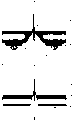
相反,露出第一配线后,划线区域成为在半导体基板上形成电路时成膜的绝缘膜露出的状态。这时在所述划线区域上只存在所述绝缘膜、树脂、玻璃基板。考虑到各部的厚度,实质上成为仅用玻璃基板支承所有半导体芯片的状态。另外,由于半导体基板的材料与玻璃基板中的热膨胀率不同,所以玻璃基板上产生大的弯曲。因此由作业中的装卸而对玻璃基板作用有粘接玻璃基板的半导体芯片等的载荷。结果如图11所示,在半导体芯片的外周部半导体芯片与未图示的玻璃基板间产生剥离204,在玻璃基板202上产生裂纹205。结果出现半导体装置的成品率和可靠性降低的问题。
如图12所示,本发明不蚀刻整个划线区域,而是仅蚀刻露出第一配线的部分。以后把露出该第一配线的部分称窗口303。其结果是未图示的玻璃基板的大部分通过未图示的树脂和绝缘膜保持与半导体基板302粘接的状态。在该状态下通过形成绝缘膜、第二配线等,最后用切割除去图12中304所示的区域而分离半导体装置。
另外,本发明中,在分离半导体装置时,沿切割线时的切断区域304的整体形成未图示的切口,再把该切口用保护膜覆盖后进行切割。
本发明具有通过防止玻璃基板上产生的裂纹和半导体芯片周边部产生的剥离而提高半导体装置成品率和可靠性的效果。另外通过把玻璃基板从两片变为一片,还能谋求半导体装置的薄型化和降低成本。
附图说明
图1是表示本发明实施方式的半导体装置制造方法的剖面图;
图2是表示本发明实施方式的半导体装置制造方法的剖面图;
图3是表示本发明实施方式的半导体装置制造方法的剖面图;
图4是表示本发明实施方式的半导体装置制造方法的剖面图;
图5是表示本发明实施方式的半导体装置制造方法的剖面图;
图6是表示本发明实施方式的半导体装置制造方法的剖面图;
图7是表示本发明实施方式的半导体装置制造方法的剖面图;
图8是表示本发明实施方式的半导体装置制造方法的剖面图;
图9是表示本发明实施方式的半导体装置制造方法的剖面图;
图10是表示本发明实施方式的半导体装置制造方法的剖面图;
图11是现有例的BGA型半导体装置制作中的平面图;
图12是本发明实施方式的半导体装置制作中的平面图;
图13是现有例BGA型半导体装置的立体图;
图14是现有例BGA型半导体装置的剖面图。
具体实施方式
以下,参照图1到图10的半导体装置的剖面图和图12的半导体装置的平面图说明本发明实施例半导体装置的制造方法。
首先如图1所示,准备半导体基板1。这些半导体基板1是通过半导体工艺过程在所述半导体基板1上形成如CCD的图像传感器和半导体存储器的。在其表面上涂敷第一绝缘膜2,然后,在用于分断成每个半导体芯片的边界S(被称切割线或划线)附近具有规定间隙并形成第一配线3。在此,第一配线3是从半导体装置的焊盘到边界S附近扩张的焊盘。即,第一配线3是外部连接焊盘,与半导体装置未图示的电路电连接。
然后,把作为支承体使用的玻璃基板4通过作为透明粘接剂的树脂5(例如环氧树脂)粘接在形成有第一配线3的半导体基板1上。在此,支承体使用玻璃基板、粘接剂使用环氧树脂,但作为支承体也可以使用硅基板和塑料板,粘接剂可选择对这些支承体合适的粘接剂。
然后,对所述半导体基板1,把粘接玻璃基板4的面的反面进行背磨,把基板的厚度变薄。在背磨的半导体基板1的面上产生擦痕,可出现宽度、深度数μm左右的凹凸。为了使其变小,则使用与作为半导体基板1的材料硅和作为第一绝缘膜2的材料硅氧化膜相比具有高蚀刻选择比的药液来进行湿蚀刻。
如前所述,作为药液,只要与硅和硅氧化膜相比具有高蚀刻选择比,就不特别的限定。例如本发明中作为硅蚀刻溶液使用氟化氢酸2.5%、硝酸50%、醋酸10%和水37.5%的溶液。
另外,最好进行该湿蚀刻,但本发明不限制不进行湿蚀刻。
然后,如图2(a)和图2(b)所示,在所述半导体基板1中对粘接玻璃基板4的面的反面以设置了开口部的未图示抗蚀图形作为掩膜进行半导体基板1的各向同性蚀刻(或各向异性蚀刻),以把第一配线3的一部分露出。其结果,一方面如图2(a)所示,在存在有第一配线3的部分中,在边界S部分形成开口的窗口20,成为露出第一绝缘膜2的状态。另一方面,如图2(b)所示,在不存在有第一配线3的部分,原封不动保留半导体基板1。结果,从半导体基板1一侧观察图2(a)和图2(b)的半导体装置时就成为如图12的平面图。
如上所述,通过设置仅能把对应于第一配线3的位置露出而得到的窗口20使半导体基板1与玻璃基板4通过第一绝缘膜2和树脂5粘接的区域增大。由此能提高由玻璃基板4的支承强度。而且可降低由半导体基板1与玻璃基板4热膨胀率的差异导致的玻璃基板4的弯曲,并降低在半导体装置中产生的裂纹和剥离。
该蚀刻可用干蚀刻、湿蚀刻的任一种进行。并且在这以后的工序说明中与图2(a)和图2(b)一样,把形成有窗口20的部分的剖面图表示为图号(a),把没形成有窗口20的部分的剖面图表示为图号(b)。
蚀刻的半导体基板1的面上有面内的凹凸和残渣、异物,并且如图2(a)中围成的圆圈1a、1b所示,窗口20中成为角的部分成为尖的形状。
因此,如图3(a)和图3(b)所示,为除去残渣和异物、把尖的部分的前端部变圆进行湿蚀刻。由此在图2(a)中围成的圆圈1a、1b的尖的部分就变成如图3(a)中围成圆形的1a、1b所示圆滑的形状。
然后如图4(a)和图4(b)所示,在所述半导体基板1中,对粘接了玻璃基板4的面的反面进行第二绝缘膜6的成膜。在本实施例,把硅烷基的氧化膜成膜3μm左右。
然后,所述半导体基板1中,对粘接玻璃基板4的面的反面涂布未图示的抗蚀剂,以使沿窗口20内的边界S的部分开口的方式形成图案,形成蚀刻膜。然后,如图5(a)和图5(b)所示,以该未图示的抗蚀膜作为掩膜进行第二绝缘膜6和第一绝缘膜2的蚀刻,使第一配线3的一部分露出。
然后,如图6(a)和图6(b)所示,以对应于以后形成导电端子11的位置的方式形成具有柔软性的缓冲部件7。另外,缓冲部件7具有吸收加在导电端子11上的力而缓和导电端子11接合时的应力的功能,但本发明不限制不使用缓冲部件7。
然后,在所述玻璃基板4的反面上形成第二配线层8。由此第一配线3与第二配线8电连接。
然后,在所述玻璃基板4的反面上涂布未图示的抗蚀剂。在此,在形成有窗口20的部分以使沿窗口20内的边界S的部分开口的方式形成抗蚀膜图形。而在窗口20没有开口的部分以使第二配线层8露出的方式形成抗蚀膜图形。然后,以所述未图示的抗蚀膜作为掩膜进行蚀刻,除去边界S附近的第二配线层8而形成第二配线8。并且,把没形成有窗口20的部分的第二配线8除去。
然后如图7(a)和图7(b)所示,以把玻璃基板4例如切削30μm左右的深度方式,沿边界S形成切口30(倒V字型的槽)。
即在半导体基板1上存在有第一配线3的部分(即沿窗口20内的边界S的部分)中切削树脂5和玻璃基板4的一部分而形成所述切口30。这时,必须使用不接触窗口20内的第二配线那样宽的刀片。
而在半导体基板1上不存在有第一配线3的区域(即没形成有窗口20的区域)切削半导体基板1、第一绝缘膜2、树脂5、和玻璃基板4的一部分而形成所述切口30。
另外,在本实施方式中,切口30的形状呈楔形的剖面形状,但也可以是矩形的剖面形状。而且本发明并不强制进行切入上述那样的切口30的工序。
然后,如图8(a)和图8(b)所示,对玻璃基板4的反面进行非电解镀敷处理,在第二配线8形成Ni-Au镀膜9。该膜由于是镀敷,所以仅在存在有第二配线8的部分形成。
然后,如图9(a)和图9(b)所示,在玻璃基板4的反面上形成保护膜10。为了形成保护膜10,把玻璃基板4的反面朝上,从上方滴下热固化性的有机系树脂,使半导体基板自身旋转,利用由该旋转产生的离心力使该有机系树脂扩展到基板面上。由此,包含沿边界S形成的切口30的内壁的半导体基板1的背面一侧形成保护膜10。
即,在半导体基板1上存在有第一配线3的部分(即沿窗口20内的边界S的部分)中,形成有保护膜10,以把从第二绝缘膜6的表面到切口30的内壁露出的树脂5和玻璃基板4覆盖。而在半导体基板1上存在有第一配线3以外的区域(即没形成有窗口20的区域)中,形成有保护膜10,以把从第二绝缘膜6的表面到切口30的内壁露出的第二绝缘膜6、半导体基板1、第一绝缘膜2、树脂5和玻璃基板4的各露出部覆盖。
然后,通过利用未图示的抗蚀掩膜(在与缓冲部件7对应的位置处具有开口部)的蚀刻把形成导电端子11部分的保护膜10除去,在对应于缓冲部件7的Ni-Au镀膜9上的位置处形成导电端子11。该导电端子11通过Ni-Au镀膜9与第二配线8电连接。导电端子11由焊锡突起和金突起形成。特别是使用金突起时能把导电端子11的厚度从160微米减少到数微米~数十微米。
然后如图10(a)和图10(b)所示,从设置了切口30的部分沿边界S进行切割,把半导体装置分离成各个的半导体芯片。这时切割中所用刀片宽度必须是仅能切削玻璃基板4和切口30内的保护膜的宽度。
如上所述,根据本实施方式的半导体装置的制造方法,其是两阶段的切割,即形成切口30,再在形成覆盖该切口30的保护膜10之后进行切割。由此因为在把半导体装置分离成各个半导体芯片而进行切割时,沿边界S(即切割线)形成的切口30的内壁用保护膜10覆盖,所以仅通过切割玻璃基板4和保护膜10就能进行分离。即刀片与玻璃基板4和保护膜10以外的层(树脂5和第二配线8等)不接触。因此能极力抑制在分离的半导体装置,即半导体芯片的断面和边缘部切割时由刀片的接触导致的剥离。
结果,能提高半导体装置的成品率和可靠性。并且本发明的半导体装置是由一片玻璃基板构成的,所以能谋求半导体装置的薄型化和降低成本。
本实施例中形成了与第二配线8电连接的导电端子11,但本发明不限于此。即本发明对不形成导电端子的半导体装置(例如LGA:Land GridArray型封装件)也适用。
Claims (10)
1.一种半导体装置的制造方法,其特征在于,具有如下工序:经由在包括多个半导体芯片的半导体基板的第一面上形成的第一绝缘膜,在从所述多个半导体芯片的边界分离开的位置上配置第一配线,通过粘接剂粘接支承体,以覆盖形成所述第一配线;
有选择地除去所述半导体基板的一部分,并使所述第一配线以及位于所述第一配线下部的所述第一绝缘膜露出而形成开口部。
2.如权利要求1所述的半导体装置的制造方法,其特征在于,所述第一配线隔着所述半导体芯片的边界配置成一对,所述开口部按所述一对第一配线的形成区域不连续地存在。
3.一种半导体装置的制造方法,其特征在于,具有如下工序:经由在包括多个半导体芯片的半导体基板的第一面上形成的第一绝缘膜,在从所述多个半导体芯片的边界分离开的位置上配置第一配线,通过粘接剂粘接支承体,以覆盖所述第一配线;
有选择地除去所述半导体基板的一部分而把所述第一绝缘膜露出;
把第二绝缘膜形成在所述半导体基板的与所述第一面相对的第二面上;
有选择地蚀刻所述第一绝缘膜和所述第二绝缘膜而使所述第一配线露出;
在所述半导体基板的第二面上形成与所述第一配线连接的第二配线;
在所述半导体基板的第二面沿所述边界切入切口;
沿所述切口进行切割而把各个所述半导体芯片进行分离。
4.如权利要求3所述的半导体装置的制造方法,其特征在于,所述第一配线隔着所述半导体芯片的边界配置成一对,有选择地除去所述半导体基板的一部分而露出所述第一绝缘膜的区域按所述一对第一配线的形成区域不连续地存在。
5.如权利要求4所述的半导体装置的制造方法,其特征在于,进行所述切割时被除去的区域的宽度小于所述一对第一配线的间隔。
6.如权利要求3或4所述的半导体装置的制造方法,其特征在于,所述切入切口工序中进行加工,以把切口切入至所述支承体。
7.如权利要求3或4所述的半导体装置的制造方法,其特征在于,其具有用保护膜覆盖所述切口的工序,在所述切割中仅切削所述保护膜和所述支承体。
8.一种半导体装置,其特征在于,包括:多个第一配线,其通过第一绝缘膜形成在切割线近旁的半导体芯片上;
支承体,其通过粘接剂粘接在包括所述第一配线上的所述第一绝缘膜上;
多个开口部,其穿透设置,以使所述第一配线从未粘接所述支承体的面的半导体芯片露出并至切割线;
第二配线,其通过所述开口部连接在所述第一配线上。
9.如权利要求8所述的半导体装置,其特征在于,在与所述切割线对应的半导体芯片的端部从所述半导体芯片到支承体切入切口。
10.如权利要求9所述的半导体装置,其特征在于,形成保护膜,以覆盖所述切口。
Applications Claiming Priority (6)
| Application Number | Priority Date | Filing Date | Title |
|---|---|---|---|
| JP2003288150 | 2003-08-06 | ||
| JP288150/03 | 2003-08-06 | ||
| JP288150/2003 | 2003-08-06 | ||
| JP022989/04 | 2004-01-30 | ||
| JP022989/2004 | 2004-01-30 | ||
| JP2004022989A JP4401181B2 (ja) | 2003-08-06 | 2004-01-30 | 半導体装置及びその製造方法 |
Related Child Applications (1)
| Application Number | Title | Priority Date | Filing Date |
|---|---|---|---|
| CN 200710197182 Division CN101174572B (zh) | 2003-08-06 | 2004-08-06 | 半导体装置及其制造方法 |
Publications (2)
| Publication Number | Publication Date |
|---|---|
| CN1581428A CN1581428A (zh) | 2005-02-16 |
| CN100367451C true CN100367451C (zh) | 2008-02-06 |
Family
ID=33554530
Family Applications (1)
| Application Number | Title | Priority Date | Filing Date |
|---|---|---|---|
| CNB2004100562611A Expired - Fee Related CN100367451C (zh) | 2003-08-06 | 2004-08-06 | 半导体装置及其制造方法 |
Country Status (6)
| Country | Link |
|---|---|
| US (2) | US7312107B2 (zh) |
| EP (1) | EP1505643B1 (zh) |
| JP (1) | JP4401181B2 (zh) |
| KR (1) | KR100636770B1 (zh) |
| CN (1) | CN100367451C (zh) |
| TW (1) | TWI236046B (zh) |
Cited By (1)
| Publication number | Priority date | Publication date | Assignee | Title |
|---|---|---|---|---|
| CN104517864A (zh) * | 2013-10-08 | 2015-04-15 | 精材科技股份有限公司 | 晶圆级晶片封装体的制造方法 |
Families Citing this family (45)
| Publication number | Priority date | Publication date | Assignee | Title |
|---|---|---|---|---|
| TWI232560B (en) | 2002-04-23 | 2005-05-11 | Sanyo Electric Co | Semiconductor device and its manufacture |
| TWI229435B (en) * | 2002-06-18 | 2005-03-11 | Sanyo Electric Co | Manufacture of semiconductor device |
| TWI227550B (en) | 2002-10-30 | 2005-02-01 | Sanyo Electric Co | Semiconductor device manufacturing method |
| JP4401181B2 (ja) | 2003-08-06 | 2010-01-20 | 三洋電機株式会社 | 半導体装置及びその製造方法 |
| JP4322181B2 (ja) * | 2004-07-29 | 2009-08-26 | 三洋電機株式会社 | 半導体装置の製造方法 |
| KR100604903B1 (ko) * | 2004-09-30 | 2006-07-28 | 삼성전자주식회사 | 단차피복성을 향상시킨 반도체 웨이퍼 및 그 제조방법 |
| JP2006278610A (ja) * | 2005-03-29 | 2006-10-12 | Sanyo Electric Co Ltd | 半導体装置及びその製造方法 |
| WO2007040688A2 (en) * | 2005-09-30 | 2007-04-12 | Bae Systems Information And Electronic Systems Integration Inc. | Cmos process for fabrication of ultra small or non standard size or shape semiconductor die |
| JP2007165696A (ja) * | 2005-12-15 | 2007-06-28 | Sanyo Electric Co Ltd | 半導体装置及びその製造方法 |
| JP5010244B2 (ja) | 2005-12-15 | 2012-08-29 | オンセミコンダクター・トレーディング・リミテッド | 半導体装置 |
| TWI324800B (en) | 2005-12-28 | 2010-05-11 | Sanyo Electric Co | Method for manufacturing semiconductor device |
| TW200737506A (en) | 2006-03-07 | 2007-10-01 | Sanyo Electric Co | Semiconductor device and manufacturing method of the same |
| JP2008003577A (ja) * | 2006-05-25 | 2008-01-10 | Canon Inc | 画像表示装置の製造方法および分断方法 |
| US8102039B2 (en) | 2006-08-11 | 2012-01-24 | Sanyo Semiconductor Co., Ltd. | Semiconductor device and manufacturing method thereof |
| US8148811B2 (en) | 2006-08-25 | 2012-04-03 | Semiconductor Components Industries, Llc | Semiconductor device and manufacturing method thereof |
| WO2008023824A1 (fr) | 2006-08-25 | 2008-02-28 | Sanyo Electric Co., Ltd. | Dispositif à semi-conducteur et son procédé de fabrication |
| WO2008023827A1 (fr) | 2006-08-25 | 2008-02-28 | Sanyo Electric Co., Ltd. | Dispositif semi-conducteur |
| US8513789B2 (en) * | 2006-10-10 | 2013-08-20 | Tessera, Inc. | Edge connect wafer level stacking with leads extending along edges |
| US7901989B2 (en) | 2006-10-10 | 2011-03-08 | Tessera, Inc. | Reconstituted wafer level stacking |
| JP4743631B2 (ja) | 2006-10-23 | 2011-08-10 | 三洋電機株式会社 | 半導体装置及びその製造方法 |
| JP5010247B2 (ja) | 2006-11-20 | 2012-08-29 | オンセミコンダクター・トレーディング・リミテッド | 半導体装置及びその製造方法 |
| US7569409B2 (en) * | 2007-01-04 | 2009-08-04 | Visera Technologies Company Limited | Isolation structures for CMOS image sensor chip scale packages |
| JP5301108B2 (ja) | 2007-04-20 | 2013-09-25 | セミコンダクター・コンポーネンツ・インダストリーズ・リミテッド・ライアビリティ・カンパニー | 半導体装置 |
| JP2008294405A (ja) | 2007-04-25 | 2008-12-04 | Sanyo Electric Co Ltd | 半導体装置及びその製造方法 |
| EP2186134A2 (en) | 2007-07-27 | 2010-05-19 | Tessera, Inc. | Reconstituted wafer stack packaging with after-applied pad extensions |
| JP2009032929A (ja) | 2007-07-27 | 2009-02-12 | Sanyo Electric Co Ltd | 半導体装置及びその製造方法 |
| KR100887479B1 (ko) * | 2007-10-09 | 2009-03-10 | 주식회사 네패스 | 내균열성 반도체 패키지 및 그 제조 방법 |
| JP2010027741A (ja) * | 2008-07-16 | 2010-02-04 | Sanyo Electric Co Ltd | 半導体装置及びその製造方法 |
| JP2010103300A (ja) | 2008-10-23 | 2010-05-06 | Sanyo Electric Co Ltd | 半導体装置及びその製造方法 |
| DE102008058003B4 (de) * | 2008-11-19 | 2012-04-05 | Infineon Technologies Ag | Verfahren zur Herstellung eines Halbleitermoduls und Halbleitermodul |
| JP5985136B2 (ja) * | 2009-03-19 | 2016-09-06 | ソニー株式会社 | 半導体装置とその製造方法、及び電子機器 |
| US8298917B2 (en) * | 2009-04-14 | 2012-10-30 | International Business Machines Corporation | Process for wet singulation using a dicing singulation structure |
| JP5475363B2 (ja) * | 2009-08-07 | 2014-04-16 | ラピスセミコンダクタ株式会社 | 半導体装置およびその製造方法 |
| US8952519B2 (en) * | 2010-01-13 | 2015-02-10 | Chia-Sheng Lin | Chip package and fabrication method thereof |
| JP2012028359A (ja) * | 2010-07-20 | 2012-02-09 | On Semiconductor Trading Ltd | 半導体装置及びその製造方法 |
| JP5656501B2 (ja) | 2010-08-06 | 2015-01-21 | セミコンダクター・コンポーネンツ・インダストリーズ・リミテッド・ライアビリティ・カンパニー | 半導体装置及びその製造方法 |
| US8722514B2 (en) | 2011-01-17 | 2014-05-13 | Infineon Technologies Ag | Semiconductor devices having insulating substrates and methods of formation thereof |
| DE102011112659B4 (de) * | 2011-09-06 | 2022-01-27 | Vishay Semiconductor Gmbh | Oberflächenmontierbares elektronisches Bauelement |
| JP2013125753A (ja) | 2011-12-13 | 2013-06-24 | Semiconductor Components Industries Llc | 半導体集積回路 |
| JP5968711B2 (ja) * | 2012-07-25 | 2016-08-10 | ルネサスエレクトロニクス株式会社 | 半導体装置及び半導体装置の製造方法 |
| CN102810549B (zh) * | 2012-08-29 | 2015-04-01 | 格科微电子(上海)有限公司 | 图像传感器的晶圆级封装的制作方法 |
| US11244908B2 (en) | 2018-11-06 | 2022-02-08 | STATS ChipPAC Pte. Ltd. | Method and device for reducing metal burrs when sawing semiconductor packages |
| JP2019091945A (ja) * | 2019-03-08 | 2019-06-13 | 三星ダイヤモンド工業株式会社 | 半田ボール付き半導体チップの製造装置及び作製方法 |
| KR20220006931A (ko) | 2020-07-09 | 2022-01-18 | 삼성전자주식회사 | 인터포저 및 이를 포함하는 반도체 패키지 |
| US20220102289A1 (en) * | 2020-09-30 | 2022-03-31 | Tokyo Electron Limited | Stress Relief in Semiconductor Wafers |
Citations (1)
| Publication number | Priority date | Publication date | Assignee | Title |
|---|---|---|---|---|
| JP2002512436A (ja) * | 1998-02-06 | 2002-04-23 | シェルケース リミティド | 集積回路デバイス |
Family Cites Families (123)
| Publication number | Priority date | Publication date | Assignee | Title |
|---|---|---|---|---|
| FR2013735A1 (zh) * | 1968-07-05 | 1970-04-10 | Gen Electric Inf Ita | |
| GB1285708A (en) * | 1968-10-28 | 1972-08-16 | Lucas Industries Ltd | Semi-conductor devices |
| US3648131A (en) * | 1969-11-07 | 1972-03-07 | Ibm | Hourglass-shaped conductive connection through semiconductor structures |
| US4179794A (en) * | 1975-07-23 | 1979-12-25 | Nippon Gakki Seizo Kabushiki Kaisha | Process of manufacturing semiconductor devices |
| US4954875A (en) * | 1986-07-17 | 1990-09-04 | Laser Dynamics, Inc. | Semiconductor wafer array with electrically conductive compliant material |
| US4978639A (en) * | 1989-01-10 | 1990-12-18 | Avantek, Inc. | Method for the simultaneous formation of via-holes and wraparound plating on semiconductor chips |
| JPH0482215A (ja) | 1990-07-25 | 1992-03-16 | Sumitomo Electric Ind Ltd | ランプアニール装置 |
| US5229647A (en) | 1991-03-27 | 1993-07-20 | Micron Technology, Inc. | High density data storage using stacked wafers |
| US5927993A (en) | 1992-02-03 | 1999-07-27 | Motorola, Inc. | Backside processing method |
| US5350662A (en) * | 1992-03-26 | 1994-09-27 | Hughes Aircraft Company | Maskless process for forming refractory metal layer in via holes of GaAs chips |
| US5476819A (en) * | 1993-07-26 | 1995-12-19 | Litton Systems, Inc. | Substrate anchor for undercut silicon on insulator microstructures |
| TW270213B (zh) | 1993-12-08 | 1996-02-11 | Matsushita Electric Ind Co Ltd | |
| IL108359A (en) * | 1994-01-17 | 2001-04-30 | Shellcase Ltd | Method and device for creating integrated circular devices |
| JPH08186151A (ja) * | 1994-12-29 | 1996-07-16 | Sony Corp | 半導体装置及びその製造方法 |
| US5682062A (en) | 1995-06-05 | 1997-10-28 | Harris Corporation | System for interconnecting stacked integrated circuits |
| US5648684A (en) * | 1995-07-26 | 1997-07-15 | International Business Machines Corporation | Endcap chip with conductive, monolithic L-connect for multichip stack |
| JPH0963993A (ja) | 1995-08-24 | 1997-03-07 | Hitachi Ltd | 半導体ウェハのダイシング方法およびダイシング装置ならびにダイオードペレットの製造方法およびダイオードペレット |
| US5904546A (en) * | 1996-02-12 | 1999-05-18 | Micron Technology, Inc. | Method and apparatus for dicing semiconductor wafers |
| KR100410812B1 (ko) | 1996-06-25 | 2004-04-01 | 주식회사 하이닉스반도체 | 반도체장치의제조방법 |
| US6027958A (en) | 1996-07-11 | 2000-02-22 | Kopin Corporation | Transferred flexible integrated circuit |
| DE19636744C2 (de) | 1996-09-10 | 1998-09-17 | Siemens Ag | Verfahren zum Übertragen von Daten in einem hybriden Telekommunikationssystem, insbesondere einem "ISDN - DECT-spezifischen RLL/WLL"-System |
| WO1998013862A1 (fr) | 1996-09-24 | 1998-04-02 | Mitsubishi Denki Kabushiki Kaisha | Dispositif a semi-conducteur et son procede de fabrication |
| US5691245A (en) * | 1996-10-28 | 1997-11-25 | He Holdings, Inc. | Methods of forming two-sided HDMI interconnect structures |
| EP2270846A3 (en) | 1996-10-29 | 2011-12-21 | ALLVIA, Inc. | Integrated circuits and methods for their fabrication |
| US6054760A (en) | 1996-12-23 | 2000-04-25 | Scb Technologies Inc. | Surface-connectable semiconductor bridge elements and devices including the same |
| US5910687A (en) | 1997-01-24 | 1999-06-08 | Chipscale, Inc. | Wafer fabrication of die-bottom contacts for electronic devices |
| JPH10242084A (ja) | 1997-02-24 | 1998-09-11 | Lintec Corp | ウェハ貼着用粘着シートおよび電子部品の製造方法 |
| IT1289965B1 (it) * | 1997-02-25 | 1998-10-19 | Ausimont Spa | Composti contenenti anello triazinico |
| JP3286553B2 (ja) | 1997-03-17 | 2002-05-27 | 株式会社村上開明堂 | 防眩インナーミラー |
| JP3011233B2 (ja) | 1997-05-02 | 2000-02-21 | 日本電気株式会社 | 半導体パッケージ及びその半導体実装構造 |
| US6051489A (en) | 1997-05-13 | 2000-04-18 | Chipscale, Inc. | Electronic component package with posts on the active side of the substrate |
| JP3335575B2 (ja) | 1997-06-06 | 2002-10-21 | 松下電器産業株式会社 | 半導体装置およびその製造方法 |
| FR2767223B1 (fr) | 1997-08-06 | 1999-09-17 | Commissariat Energie Atomique | Procede d'interconnexion a travers un materiau semi-conducteur, et dispositif obtenu |
| US6432744B1 (en) | 1997-11-20 | 2002-08-13 | Texas Instruments Incorporated | Wafer-scale assembly of chip-size packages |
| EP0926723B1 (en) * | 1997-11-26 | 2007-01-17 | STMicroelectronics S.r.l. | Process for forming front-back through contacts in micro-integrated electronic devices |
| US5888884A (en) * | 1998-01-02 | 1999-03-30 | General Electric Company | Electronic device pad relocation, precision placement, and packaging in arrays |
| EP1041617A4 (en) | 1998-01-20 | 2001-07-18 | Citizen Watch Co Ltd | SEMICONDUCTOR DEVICE AND METHOD FOR PRODUCING THE SAME, AND STRUCTURE AND METHOD FOR FIXING SEMICONDUCTOR |
| US6624505B2 (en) | 1998-02-06 | 2003-09-23 | Shellcase, Ltd. | Packaged integrated circuits and methods of producing thereof |
| JP3497722B2 (ja) * | 1998-02-27 | 2004-02-16 | 富士通株式会社 | 半導体装置及びその製造方法及びその搬送トレイ |
| US7205181B1 (en) * | 1998-03-20 | 2007-04-17 | Mcsp, Llc | Method of forming hermetic wafer scale integrated circuit structure |
| JP3842444B2 (ja) | 1998-07-24 | 2006-11-08 | 富士通株式会社 | 半導体装置の製造方法 |
| US6153929A (en) | 1998-08-21 | 2000-11-28 | Micron Technology, Inc. | Low profile multi-IC package connector |
| DE19846232A1 (de) * | 1998-09-03 | 2000-03-09 | Fraunhofer Ges Forschung | Verfahren zur Herstellung eines Halbleiterbauelements mit Rückseitenkontaktierung |
| US6066513A (en) * | 1998-10-02 | 2000-05-23 | International Business Machines Corporation | Process for precise multichip integration and product thereof |
| US6339251B2 (en) * | 1998-11-10 | 2002-01-15 | Samsung Electronics Co., Ltd | Wafer grooves for reducing semiconductor wafer warping |
| JP2000173952A (ja) * | 1998-12-03 | 2000-06-23 | Fujitsu Quantum Device Kk | 半導体装置及びその製造方法 |
| US6310328B1 (en) | 1998-12-10 | 2001-10-30 | Mattson Technologies, Inc. | Rapid thermal processing chamber for processing multiple wafers |
| JP3687379B2 (ja) | 1998-12-18 | 2005-08-24 | 株式会社日立製作所 | 半導体装置の製造方法 |
| KR100315030B1 (ko) * | 1998-12-29 | 2002-04-24 | 박종섭 | 반도체패키지의제조방법 |
| US6259039B1 (en) | 1998-12-29 | 2001-07-10 | Intel Corporation | Surface mount connector with pins in vias |
| FR2788375B1 (fr) | 1999-01-11 | 2003-07-18 | Gemplus Card Int | Procede de protection de puce de circuit integre |
| JP2000286283A (ja) | 1999-03-30 | 2000-10-13 | Seiko Epson Corp | 半導体装置の製造方法 |
| KR100416174B1 (ko) * | 1999-03-31 | 2004-01-24 | 세이코 엡슨 가부시키가이샤 | 반도체 장치의 제조 방법 |
| JP2000294677A (ja) | 1999-04-05 | 2000-10-20 | Fujitsu Ltd | 高密度薄膜配線基板及びその製造方法 |
| US6326689B1 (en) * | 1999-07-26 | 2001-12-04 | Stmicroelectronics, Inc. | Backside contact for touchchip |
| WO2001009932A1 (fr) * | 1999-07-30 | 2001-02-08 | Nippon Sheet Glass Co., Ltd. | Procede de decoupage de plaquette de semi-conducteur en puces et structure de rainure formee dans la zone de decoupage |
| JP3687435B2 (ja) | 1999-08-27 | 2005-08-24 | セイコーエプソン株式会社 | 半導体チップおよびその製造方法、半導体装置、コンピュータ、回路基板ならびに電子機器 |
| KR100462980B1 (ko) | 1999-09-13 | 2004-12-23 | 비쉐이 메저먼츠 그룹, 인코포레이티드 | 반도체장치용 칩 스케일 표면 장착 패키지 및 그 제조공정 |
| US6316287B1 (en) * | 1999-09-13 | 2001-11-13 | Vishay Intertechnology, Inc. | Chip scale surface mount packages for semiconductor device and process of fabricating the same |
| JP2001127243A (ja) | 1999-10-26 | 2001-05-11 | Sharp Corp | 積層半導体装置 |
| JP2001185519A (ja) | 1999-12-24 | 2001-07-06 | Hitachi Ltd | 半導体装置及びその製造方法 |
| JP3858545B2 (ja) | 1999-12-27 | 2006-12-13 | セイコーエプソン株式会社 | 半導体モジュール及び電子機器 |
| JP2001210667A (ja) | 2000-01-28 | 2001-08-03 | New Japan Radio Co Ltd | 半導体装置の製造方法 |
| US6534751B2 (en) | 2000-02-28 | 2003-03-18 | Kyocera Corporation | Wafer heating apparatus and ceramic heater, and method for producing the same |
| US6424031B1 (en) | 2000-05-08 | 2002-07-23 | Amkor Technology, Inc. | Stackable package with heat sink |
| JP3701542B2 (ja) | 2000-05-10 | 2005-09-28 | シャープ株式会社 | 半導体装置およびその製造方法 |
| JP3879816B2 (ja) | 2000-06-02 | 2007-02-14 | セイコーエプソン株式会社 | 半導体装置及びその製造方法、積層型半導体装置、回路基板並びに電子機器 |
| JP4329235B2 (ja) | 2000-06-27 | 2009-09-09 | セイコーエプソン株式会社 | 半導体装置及びその製造方法 |
| JP2002026270A (ja) * | 2000-07-10 | 2002-01-25 | Nec Corp | 半導体装置の製造方法 |
| JP2002094082A (ja) | 2000-07-11 | 2002-03-29 | Seiko Epson Corp | 光素子及びその製造方法並びに電子機器 |
| JP2002057128A (ja) * | 2000-08-15 | 2002-02-22 | Fujitsu Quantum Devices Ltd | 半導体装置及びその製造方法 |
| US6379982B1 (en) | 2000-08-17 | 2002-04-30 | Micron Technology, Inc. | Wafer on wafer packaging and method of fabrication for full-wafer burn-in and testing |
| US6406934B1 (en) | 2000-09-05 | 2002-06-18 | Amkor Technology, Inc. | Wafer level production of chip size semiconductor packages |
| JP2002083785A (ja) | 2000-09-07 | 2002-03-22 | Nec Kansai Ltd | 半導体素子の製造方法 |
| JP2002093942A (ja) | 2000-09-14 | 2002-03-29 | Nec Corp | 半導体装置およびその製造方法 |
| JP4183375B2 (ja) | 2000-10-04 | 2008-11-19 | 沖電気工業株式会社 | 半導体装置及びその製造方法 |
| US6693358B2 (en) * | 2000-10-23 | 2004-02-17 | Matsushita Electric Industrial Co., Ltd. | Semiconductor chip, wiring board and manufacturing process thereof as well as semiconductor device |
| JP2002163900A (ja) | 2000-11-22 | 2002-06-07 | Hitachi Ltd | 半導体ウエハ、半導体チップ、半導体装置および半導体装置の製造方法 |
| US6506681B2 (en) | 2000-12-06 | 2003-01-14 | Micron Technology, Inc. | Thin flip—chip method |
| US6524885B2 (en) * | 2000-12-15 | 2003-02-25 | Eaglestone Partners I, Llc | Method, apparatus and system for building an interposer onto a semiconductor wafer using laser techniques |
| JP2002231918A (ja) | 2001-02-06 | 2002-08-16 | Olympus Optical Co Ltd | 固体撮像装置及びその製造方法 |
| US6399463B1 (en) * | 2001-03-01 | 2002-06-04 | Amkor Technology, Inc. | Method of singulation using laser cutting |
| JP4497737B2 (ja) | 2001-03-12 | 2010-07-07 | 株式会社ルネサステクノロジ | 半導体装置の製造方法 |
| US6910268B2 (en) | 2001-03-27 | 2005-06-28 | Formfactor, Inc. | Method for fabricating an IC interconnect system including an in-street integrated circuit wafer via |
| US6597059B1 (en) | 2001-04-04 | 2003-07-22 | Amkor Technology, Inc. | Thermally enhanced chip scale lead on chip semiconductor package |
| JP4698877B2 (ja) | 2001-04-27 | 2011-06-08 | オリンパス株式会社 | 撮像装置 |
| US6753936B2 (en) | 2001-05-17 | 2004-06-22 | Dai Nippon Pringing Co., Ltd. | Field sequential color liquid crystal display device |
| JP2003031647A (ja) | 2001-07-19 | 2003-01-31 | Hitachi Kokusai Electric Inc | 基板処理装置および半導体装置の製造方法 |
| JP4000507B2 (ja) | 2001-10-04 | 2007-10-31 | ソニー株式会社 | 固体撮像装置の製造方法 |
| SG102639A1 (en) | 2001-10-08 | 2004-03-26 | Micron Technology Inc | Apparatus and method for packing circuits |
| US6642127B2 (en) | 2001-10-19 | 2003-11-04 | Applied Materials, Inc. | Method for dicing a semiconductor wafer |
| US6611052B2 (en) * | 2001-11-16 | 2003-08-26 | Micron Technology, Inc. | Wafer level stackable semiconductor package |
| US6955989B2 (en) * | 2001-11-30 | 2005-10-18 | Xerox Corporation | Use of a U-groove as an alternative to using a V-groove for protection against dicing induced damage in silicon |
| US6607941B2 (en) * | 2002-01-11 | 2003-08-19 | National Semiconductor Corporation | Process and structure improvements to shellcase style packaging technology |
| US6908784B1 (en) | 2002-03-06 | 2005-06-21 | Micron Technology, Inc. | Method for fabricating encapsulated semiconductor components |
| US6848177B2 (en) | 2002-03-28 | 2005-02-01 | Intel Corporation | Integrated circuit die and an electronic assembly having a three-dimensional interconnection scheme |
| TWI232560B (en) * | 2002-04-23 | 2005-05-11 | Sanyo Electric Co | Semiconductor device and its manufacture |
| US7340181B1 (en) * | 2002-05-13 | 2008-03-04 | National Semiconductor Corporation | Electrical die contact structure and fabrication method |
| JP2003332270A (ja) * | 2002-05-15 | 2003-11-21 | Renesas Technology Corp | 半導体装置およびその製造方法 |
| TWI229435B (en) * | 2002-06-18 | 2005-03-11 | Sanyo Electric Co | Manufacture of semiconductor device |
| US7399683B2 (en) | 2002-06-18 | 2008-07-15 | Sanyo Electric Co., Ltd. | Manufacturing method of semiconductor device |
| US6805279B2 (en) | 2002-06-27 | 2004-10-19 | Taiwan Semiconductor Manufacturing Co., Ltd. | Fluxless bumping process using ions |
| DE10238444B4 (de) * | 2002-08-22 | 2011-05-12 | United Monolithic Semiconductors Gmbh | Verfahren zur Herstellung von vereinzelten monolithisch integrierten Halbleiterschaltungen |
| US6903442B2 (en) | 2002-08-29 | 2005-06-07 | Micron Technology, Inc. | Semiconductor component having backside pin contacts |
| JP4081666B2 (ja) * | 2002-09-24 | 2008-04-30 | セイコーエプソン株式会社 | 半導体装置及びその製造方法、回路基板並びに電子機器 |
| TWI227050B (en) * | 2002-10-11 | 2005-01-21 | Sanyo Electric Co | Semiconductor device and method for manufacturing the same |
| TWI227550B (en) * | 2002-10-30 | 2005-02-01 | Sanyo Electric Co | Semiconductor device manufacturing method |
| JP2004165312A (ja) * | 2002-11-12 | 2004-06-10 | Sanyo Electric Co Ltd | 半導体集積装置及びその製造方法 |
| TWI239607B (en) * | 2002-12-13 | 2005-09-11 | Sanyo Electric Co | Method for making a semiconductor device |
| JP2004288816A (ja) * | 2003-03-20 | 2004-10-14 | Seiko Epson Corp | 半導体ウエハ、半導体装置及びその製造方法、回路基板並びに電子機器 |
| TWI229890B (en) | 2003-04-24 | 2005-03-21 | Sanyo Electric Co | Semiconductor device and method of manufacturing same |
| JP2004363478A (ja) * | 2003-06-06 | 2004-12-24 | Sanyo Electric Co Ltd | 半導体装置の製造方法 |
| KR101078621B1 (ko) | 2003-07-03 | 2011-11-01 | 테쎄라 테크놀로지스 아일랜드 리미티드 | 집적회로 디바이스를 패키징하기 위한 방법 및 장치 |
| JP4401181B2 (ja) | 2003-08-06 | 2010-01-20 | 三洋電機株式会社 | 半導体装置及びその製造方法 |
| JP4248355B2 (ja) * | 2003-09-24 | 2009-04-02 | 三洋電機株式会社 | 半導体装置および半導体装置の製造方法 |
| TWI226090B (en) * | 2003-09-26 | 2005-01-01 | Advanced Semiconductor Eng | Transparent packaging in wafer level |
| JP2005191550A (ja) | 2003-12-01 | 2005-07-14 | Tokyo Ohka Kogyo Co Ltd | 基板の貼り付け方法 |
| US7183137B2 (en) * | 2003-12-01 | 2007-02-27 | Taiwan Semiconductor Manufacturing Company | Method for dicing semiconductor wafers |
| JP4753170B2 (ja) * | 2004-03-05 | 2011-08-24 | 三洋電機株式会社 | 半導体装置及びその製造方法 |
| JP2006093367A (ja) * | 2004-09-24 | 2006-04-06 | Sanyo Electric Co Ltd | 半導体装置の製造方法 |
| KR100676493B1 (ko) | 2004-10-08 | 2007-02-01 | 디엔제이 클럽 인코 | 재배선 기판을 이용한 웨이퍼 레벨 칩 스케일 패키지의제조 방법 |
| US7449779B2 (en) * | 2005-03-22 | 2008-11-11 | Tessera, Inc. | Wire bonded wafer level cavity package |
| TWI324800B (en) | 2005-12-28 | 2010-05-11 | Sanyo Electric Co | Method for manufacturing semiconductor device |
-
2004
- 2004-01-30 JP JP2004022989A patent/JP4401181B2/ja not_active Expired - Fee Related
- 2004-07-28 TW TW093122499A patent/TWI236046B/zh not_active IP Right Cessation
- 2004-07-30 KR KR1020040060057A patent/KR100636770B1/ko not_active IP Right Cessation
- 2004-08-04 US US10/910,805 patent/US7312107B2/en active Active
- 2004-08-06 EP EP04018715A patent/EP1505643B1/en not_active Expired - Fee Related
- 2004-08-06 CN CNB2004100562611A patent/CN100367451C/zh not_active Expired - Fee Related
-
2007
- 2007-12-13 US US11/956,160 patent/US7919875B2/en active Active
Patent Citations (1)
| Publication number | Priority date | Publication date | Assignee | Title |
|---|---|---|---|---|
| JP2002512436A (ja) * | 1998-02-06 | 2002-04-23 | シェルケース リミティド | 集積回路デバイス |
Cited By (1)
| Publication number | Priority date | Publication date | Assignee | Title |
|---|---|---|---|---|
| CN104517864A (zh) * | 2013-10-08 | 2015-04-15 | 精材科技股份有限公司 | 晶圆级晶片封装体的制造方法 |
Also Published As
| Publication number | Publication date |
|---|---|
| EP1505643A3 (en) | 2009-05-06 |
| TWI236046B (en) | 2005-07-11 |
| KR20050016041A (ko) | 2005-02-21 |
| TW200507040A (en) | 2005-02-16 |
| US20080093708A1 (en) | 2008-04-24 |
| JP2005072554A (ja) | 2005-03-17 |
| US20050048740A1 (en) | 2005-03-03 |
| CN1581428A (zh) | 2005-02-16 |
| JP4401181B2 (ja) | 2010-01-20 |
| EP1505643A2 (en) | 2005-02-09 |
| US7919875B2 (en) | 2011-04-05 |
| EP1505643B1 (en) | 2012-11-14 |
| KR100636770B1 (ko) | 2006-10-23 |
| US7312107B2 (en) | 2007-12-25 |
Similar Documents
| Publication | Publication Date | Title |
|---|---|---|
| CN100367451C (zh) | 半导体装置及其制造方法 | |
| US7271466B2 (en) | Semiconductor device with sidewall wiring | |
| KR101173075B1 (ko) | 집적 회로 디바이스를 패키징하는 방법 및 장치 | |
| KR100661042B1 (ko) | 반도체 장치의 제조 방법 | |
| CN101355058B (zh) | 半导体装置及其制造方法 | |
| US6753238B2 (en) | Semiconductor device and manufacturing method thereof | |
| CN101295686B (zh) | 半导体装置及其制造方法 | |
| US6046073A (en) | Process for producing very thin semiconductor chips | |
| US7416920B2 (en) | Semiconductor device protective structure and method for fabricating the same | |
| EP1478021B1 (en) | Semiconductor device and manufacturing method thereof | |
| JPH11150090A (ja) | 半導体装置の製造方法 | |
| KR20050054864A (ko) | 반도체 장치 및 그 제조 방법 | |
| CN101174572B (zh) | 半导体装置及其制造方法 | |
| JP4371719B2 (ja) | 半導体装置及びその製造方法 | |
| JP4522213B2 (ja) | 半導体装置の製造方法 | |
| JP2008078165A (ja) | 半導体デバイス保護構造体及びその製造方法 | |
| KR200148753Y1 (ko) | 반도체 패키지 | |
| JP2006108254A (ja) | 半導体チップの製造方法および半導体装置の製造方法 | |
| JP2006173198A (ja) | 半導体装置及びその製造方法 | |
| JP2006179709A (ja) | 半導体装置の製造方法 | |
| JP2005101411A (ja) | 半導体装置及びその製造方法 |
Legal Events
| Date | Code | Title | Description |
|---|---|---|---|
| C06 | Publication | ||
| PB01 | Publication | ||
| C10 | Entry into substantive examination | ||
| SE01 | Entry into force of request for substantive examination | ||
| C14 | Grant of patent or utility model | ||
| GR01 | Patent grant | ||
| CF01 | Termination of patent right due to non-payment of annual fee | ||
| CF01 | Termination of patent right due to non-payment of annual fee |
Granted publication date: 20080206 Termination date: 20210806 |